
Instruction Manual


3
3600H–DFLASH–11/2012
AT26DF081A
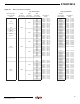
2. Pin Descriptions and Pinouts
Table 2-1. Pin Descriptions
Symbol Name and Function
Asserted
State Type
CS
CHIP SELECT: Asserting the
CS pin selects the device. When the CS pin is deasserted, the
device will be deselected and normally be placed in standby mode (not Deep Power-down mode),
and the SO pin will be in a high-impedance state. When the device is deselected, data will not be
accepted on the SI pin.
A high-to-low transition on the
CS pin is required to start an operation, and a low-to-high transition
is required to end an operation. When ending an internally self-timed operation such as a program
or erase cycle, the device will not enter the standby mode until the completion of the operation.
Low Input
SCK
SERIAL CLOCK: This pin is used to provide a clock to the device and is used to control the flow of
data to and from the device. Command, address, and input data present on the SI pin is always
latched on the rising edge of SCK, while output data on the SO pin is always clocked out on the
falling edge of SCK.
Input
SI
SERIAL INPUT: The SI pin is used to shift data into the device. The SI pin is used for all data input
including command and address sequences. Data on the SI pin is always latched on the rising
edge of SCK.
Input
SO
SERIAL OUTPUT: The SO pin is used to shift data out from the device. Data on the SO pin is
always clocked out on the falling edge of SCK.
Output
WP
WRITE PROTECT: The
WP pin controls the hardware locking feature of the device. Please refer to
section “Protection Commands and Features” on page 15 for more details on protection features
and the
WP pin.
The
WP pin is internally pulled-high and may be left floating if hardware-controlled protection will
not be used. However, it is recommended that the
WP pin also be externally connected to V
CC
whenever possible.
Low Input
HOLD
HOLD: The
HOLD pin is used to temporarily pause serial communication without deselecting or
resetting the device. While the
HOLD pin is asserted, transitions on the SCK pin and data on the
SI pin will be ignored, and the SO pin will be in a high-impedance state.
The
CS pin must be asserted, and the SCK pin must be in the low state in order for a Hold
condition to start. A Hold condition pauses serial communication only and does not have an effect
on internally self-timed operations such as a program or erase cycle. Please refer to section “Hold”
on page 30 for additional details on the Hold operation.
The
HOLD pin is internally pulled-high and may be left floating if the Hold function will not be used.
However, it is recommended that the
HOLD pin also be externally connected to V
CC
whenever
possible.
Low Input
V
CC
DEVICE POWER SUPPLY: The V
CC
pin is used to supply the source voltage to the device.
Operations at invalid V
CC
voltages may produce spurious results and should not be attempted.
Power
GND
GROUND: The ground reference for the power supply. GND should be connected to the
system ground.
Power