
Instruction Manual


32
3600H–DFLASH–11/2012
AT26DF081A
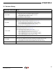
Notes: 1. Not 100% tested (value guaranteed by design and characterization).
2. 15 pF load at 70 MHz, 30 pF load at 66 MHz.
3. Only applicable as a constraint for the Write Status Register command when SPRL = 1
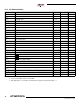
12.4 AC Characteristics
Symbol Parameter Min Max Units
f
SCK
Serial Clock (SCK) Frequency 70 MHz
f
RDLF
SCK Frequency for Read Array (Low Frequency - 03h opcode) 33 MHz
t
SCKH
SCK High Time 6.4 ns
t
SCKL
SCK Low Time 6.4 ns
t
SCKR
(1)
SCK Rise Time, Peak-to-Peak (Slew Rate) 0.1 V/ns
t
SCKF
(1)
SCK Fall Time, Peak-to-Peak (Slew Rate) 0.1 V/ns
t
CSH
Chip Select High Time 50 ns
t
CSLS
Chip Select Low Setup Time (relative to SCK) 5 ns
t
CSLH
Chip Select Low Hold Time (relative to SCK) 5 ns
t
CSHS
Chip Select High Setup Time (relative to SCK) 5 ns
t
CSHH
Chip Select High Hold Time (relative to SCK) 5 ns
t
DS
Data In Setup Time 2 ns
t
DH
Data In Hold Time 3 ns
t
DIS
(1)
Output Disable Time 6 ns
t
V
(2)
Output Valid Time 6ns
t
OH
Output Hold Time 0 ns
t
HLS
HOLD Low Setup Time (relative to SCK) 5 ns
t
HLH
HOLD Low Hold Time (relative to SCK) 5 ns
t
HHS
HOLD High Setup Time (relative to SCK) 5 ns
t
HHH
HOLD High Hold Time (relative to SCK) 5 ns
t
HLQZ
(1)
HOLD Low to Output High-Z 6 ns
t
HHQX
(1)
HOLD High to Output Low-Z 6 ns
t
WPS
(1)(3)
Write Protect Setup Time 20 ns
t
WPH
(1)(3)
Write Protect Hold Time 100 ns
t
SECP
(1)
Sector Protect Time (from Chip Select High) 20 ns
t
SECUP
(1)
Sector Unprotect Time (from Chip Select High) 20 ns
t
EDPD
(1)
Chip Select High to Deep Power-down 3 µs
t
RDPD
(1)
Chip Select High to Standby Mode 3 µs