
Instruction Manual


4
3600H–DFLASH–11/2012
AT26DF081A
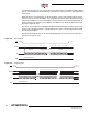
3. Block Diagram
4. Memory Array
To provide the greatest flexibility, the memory array of the AT26DF081A can be erased in four
levels of granularity including a full chip erase. In addition, the array has been divided into phys-
ical sectors of various sizes, of which each sector can be individually protected from program
and erase operations. The sizes of the physical sectors are optimized for both code and data
storage applications, allowing both code and data segments to reside in their own isolated
regions. Figure 4-1 on page 5 illustrates the breakdown of each erase level as well as the break-
down of each physical sector.
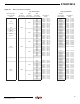
Figure 2-1. 8-SOIC Top View
1
2
3
4
8
7
6
5
CS
SO
WP
GND
VCC
HOLD
SCK
SI
FLASH
MEMORY
ARRAY
Y-GATING
CS
SCK
SO
SI
Y-DECODER
ADDRESS LATCH
X-DECODER
I/O BUFFERS
AND LATCHES
CONTROL AND
PROTECTION LOGIC
SRAM
DATA BUFFER
WP
INTERFACE
CONTROL
AND
LOGIC