Features • Ultra High Performance • • • • • • • • • – System Speeds to 100 MHz – Array Multipliers > 50 MHz – 10 ns Flexible SRAM – Internal Tri-state Capability in Each Cell FreeRAM™ – Flexible, Single/Dual Port, Synchronous/Asynchronous 10 ns SRAM – 2,048 - 18,432 Bits of Distributed SRAM Independent of Logic Cells 128 - 384 PCI Compliant I/Os – 3V/5V Capability – Programmable Output Drive – Fast, Flexible Array Access Facilitates Pin Locking – Pin-compatible with XC4000, XC5200 FPGAs 8 Global Cloc
Table 1. AT40K/AT40KLV Family(1) Device Usable Gates Rows x Columns Cells AT40K10 AT40K10LV AT40K20 AT40K20LV AT40K40 AT40K40LV 5K - 10K 10K - 20K 20K - 30K 40K - 50K 16 x 16 24 x 24 32 x 32 48 x 48 256 576 1,024 2,304 (1) (1) (1) 2,304(1) Registers 256 576 RAM Bits 2,048 4,608 8,192 18,432 128 192 256 384 I/O (Maximum) Note: Description AT40K05 AT40K05LV 1,024 1. Packages with FCK will have 8 less registers.
AT40K/AT40KLV Series FPGA Cache Logic Design The AT40K/AT40KLV, AT6000 and FPSLIC families are capable of implementing Cache Logic (dynamic full/partial logic reconfiguration, without loss of data, on-the-fly) for building adaptive logic and systems. As new logic functions are required, they can be loaded into the logic cache without losing the data already there or disrupting the operation of the rest of the chip; replacing or complementing the active logic.
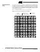
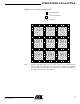
The Symmetrical Array At the heart of the Atmel architecture is a symmetrical array of identical cells, see Figure 1. The array is continuous from one edge to the other, except for bus repeaters spaced every four cells, see Figure 2 on page 5. At the intersection of each repeater row and column there is a 32 x 4 RAM block accessible by adjacent buses. The RAM can be configured as either a single-ported or dual-ported RAM(1), with either synchronous or asynchronous operation. Note: 1.
AT40K/AT40KLV Series FPGA Figure 2.
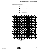
The Busing Network Figure 3 on page 7 depicts one of five identical busing planes. Each plane has three bus resources: a local-bus resource (the middle bus) and two express-bus (both sides) resources. Bus resources are connected via repeaters. Each repeater has connections to two adjacent local-bus segments and two express-bus segments. Each local-bus segment spans four cells and connects to consecutive repeaters. Each express-bus segment spans eight cells and “leapfrogs” or bypasses a repeater.
AT40K/AT40KLV Series FPGA Figure 3.
Cell Connections Figure 4(a) depicts direct connections between a cell and its eight nearest neighbors. Figure 4(b) shows the connections between a cell and five horizontal local buses (1 per busing plane) and five vertical local buses (1 per busing plane). CELL CELL CELL Plane 5 Plane 4 Plane 3 Plane 2 Plane 1 Plane 5 Plane 4 Plane 3 Plane 2 Plane 1 Figure 4.
AT40K/AT40KLV Series FPGA Figure 5.
A B C D LUT Figure 6. Some Single Cell Modes Q (Registered) DQ and/or Q LUT SUM or A B C DQ SUM (Registered) LUT LUT and/or A B C D DSP/Multiplier Mode. This mode is used to efficiently DQ PRODUCT (Registered) implement array multipliers. An array multiplier is an array or of bitwise multipliers, each implemented as a full adder LUT LUT and/or CARRY DQ Q 2:1 MUX LUT and/or A B C Arithmetic Mode is frequently used in many designs.
AT40K/AT40KLV Series FPGA RAM 32 x 4 dual-ported RAM blocks are dispersed throughout the array, see Figure 7. A 4-bit Input Data Bus connects to four horizontal local buses distributed over four sector rows (plane 1). A 4-bit Output Data Bus connects to four horizontal local buses distributed over four sectors in the same column. A 5-bit Output Address Bus connects to five vertical express buses in the same column.
Reading and writing of the 10 ns 32 x 4 dual-port FreeRAM are independent of each other. Reading the 32 x 4 dual-port RAM is completely asynchronous. Latches are transparent; when Load is logic 1, data flows through; when Load is logic 0, data is latched. These latches are used to synchronize Write Address, Write Enable Not, and Din signals for a synchronous RAM. Each bit in the 32 x 4 dual-port RAM is also a transparent latch.
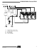
0896C–FPGA–04/02 Write Address 2-to-4 Decoder 2-to-4 Decoder Read Address Dout(0) Din(1) Dout(1) Din(2) Dout(2) Din(3) Dout(3) Din Ain Dout Aout WEN OEN Din Aout Dout Ain WEN OEN Din Ain Dout Aout WEN OEN Din Aout Dout Ain WEN OEN Din(4) Dout(4) Din(5) Dout(5) Din(6) Dout(6) Din(7) Dout(7) Din Ain WEN OEN Dout Aout Din Aout WEN OEN Dout Ain Din Ain WEN OEN Dout Aout Din Aout WEN OEN Dout Ain Local Buses Express Buses Dedicated Connections 13 AT40K/AT40KLV Series FPGA
Clocking Scheme There are eight Global Clock buses (GCK1 - GCK8) on the AT40K/AT40KLV FPGA. Each of the eight dedicated Global Clock buses is connected to one of the dual-use Global Clock pins. Any clocks used in the design should use global clocks where possible: this can be done by using Assign Pin Locks to lock the clocks to the Global Clock locations. In addition to the eight Global Clocks, there are four Fast Clocks (FCK1 - FCK4), two per edge column of the array for PCI specification.
AT40K/AT40KLV Series FPGA Figure 10.
Set/Reset Scheme The AT40K/AT40KLV family reset scheme is essentially the same as the clock scheme except that there is only one Global Reset. A dedicated Global Set/Reset bus can be driven by any User I/O, except those used for clocking (Global Clocks or Fast Clocks). The automatic placement tool will choose the reset net with the most connections to use the global resources. You can change this by using an RSBUF component in your design to indicate the global reset.
AT40K/AT40KLV Series FPGA Figure 11.
I/O Structure PAD The I/O pad is the one that connects the I/O to the outside world. Note that not all I/Os have pads: the ones without pads are called Unbonded I/Os. The number of unbonded I/Os varies with the device size and package. These unbonded I/Os are used to perform a variety of bus turns at the edge of the array. PULL-UP/PULL-DOWN Each pad has a programmable pull-up and pull-down attached to it. This supplies a weak “1” or “0” level to the pad pin.
AT40K/AT40KLV Series FPGA Primary, Secondary and Corner I/Os The AT40K/AT40KLV has three kinds of I/Os: Primary I/O, Secondary I/O and a Corner I/O. Every edge cell except corner cells on the AT40K/AT40KLV has access to one Primary I/O and two Secondary I/Os. Primary I/O Every logic cell at the edge of the FPGA array has a direct orthogonal connection to and from a Primary I/O cell. The Primary I/O interfaces directly to its adjacent core cell.
Figure 12.
AT40K/AT40KLV Series FPGA Figure 13.
“0” “1” “0” “1” “0” “1” DRIVE PULL-DOWN GND TTL/CMOS DRIVE SCHMITT DELAY “0” “1” DRIVE TRI-STATE VCC TTL/CMOS SCHMITT TRI-STATE DELAY TRI-STATE VCC PULL-UP GND PAD “1” VCC “0” PAD PULL-DOWN PULL-UP Figure 14.
AT40K/AT40KLV Series FPGA Absolute Maximum Ratings – 5V Commercial/Industrial* AT40K Operating Temperature.................................. -55°C to +125 °C *NOTICE: Storage Temperature ..................................... -65 °C to +150°C Voltage on Any Pin with Respect to Ground .................................-0.5V to V CC +7V Supply Voltage (VCC ) .........................................-0.5V to +7.
DC Characteristics – 5V Operation Commercial/Industrial/Military AT40K Symbol Parameter VIH High-level Input Voltage VIL Low-level Input Voltage Conditions Minimum CMOS 70% VCC V TTL 2.0 V CMOS -0.3 30% VCC V TTL -0.3 0.8 V IOH = 6mA VCC = VCC Minimum VOH High-level Output Voltage IOH = 14mA VCC = VCC Minimum IOH = 20mA Commercial = 4.75V Industrial/Military = 4.
AT40K/AT40KLV Series FPGA AC Timing Characteristics – 5V Operation AT40K Delays are based on fixed loads and are described in the notes. Maximum times based on worst case: VCC = 4.75V, temperature = 70°C Minimum times based on best case: VCC = 5.25V, temperature = 0°C Maximum delays are the average of tPDLH and tPDHL. Cell Function Parameter Path -2 Units Notes 2-input Gate tPD (Maximum) x/y -> x/y 1.8 ns 1 unit load 3-input Gate tPD (Maximum) x/y/z -> x/y 2.
AC Timing Characteristics – 5V Operation AT40K Delays are based on fixed loads and are described in the notes. Maximum times based on worst case: VCC = 4.75V, temperature = 70°C Minimum times based on best case: VCC = 5.25V, temperature = 0°C Maximum delays are the average of tPDLH and tPDHL. All input IO characteristics measured from a VIH of 50% of VDD at the pad (CMOS threshold) to the internal VIH of 50% of VCC.
AT40K/AT40KLV Series FPGA AC Timing Characteristics – 5V Operation AT40K Delays are based on fixed loads and are described in the notes. Maximum times based on worst case: VCC = 4.75V, temperature = 70°C Minimum times based on best case: VCC = 5.25V, temperature = 0°C Maximum delays are the average of tPDLH and tPDHL. Clocks and Reset Input buffers are measured from a VIH of 1.5V at the input pad to the internal VIH of 50% of VCC.
AC Timing Characteristics – 5V Operation AT40K Delays are based on fixed loads and are described in the notes. Maximum times based on worst case: VCC = 4.75V, temperature = 70°C Minimum times based on best case: VCC = 5.25V, temperature = 0°C Maximum delays are the average of tPDLH and tPDHL. Cell Function Parameter Path -2 Units Notes Write tWECYC (Minimum) cycle time 8.0 ns Write tWEL (Minimum) we 3.0 ns Pulse width low Write tWEH (Minimum) we 3.
AT40K/AT40KLV Series FPGA FreeRAM Asynchronous Timing Characteristics Single-port Write/Read tWEL WE ADDR tAWS tAWH 0 1 2 3 tOH OE tOXZ tDS tOZX tDH tAD DATA Dual-port Write with Read tWECYC tWEH tWEL WE WR ADDR tAWS tAWH 0 1 2 tDH WR DATA PREV. NEW tDD RD ADDR RD DATA = WR ADDR 1 tWD OLD PREV.
FreeRAM Synchronous Timing Characteristics Single-port Write/Read tCLKH CLK tWCS tWCH tACS tACH WE ADDR 0 1 3 2 OE tOXZ tDCS tDCH tOZX tAD DATA Dual-port Write with Read tCYC tCLKH tCLKL CLK tWCS tWCH tACS tACH WE WR ADDR 0 1 2 tDCS tDCH WR DATA RD ADDR = WR ADDR 1 tCD RD DATA Dual-port Read 0 RD ADDR 1 OE tOZX tAD tOXZ DATA 30 AT40K/AT40KLV Series FPGA 0896C–FPGA–04/02
AT40K/AT40KLV Series FPGA Absolute Maximum Ratings – 3.3V Commercial/Industrial* AT40KLV Operating Temperature.................................. -55°C to +125 °C Storage Temperature ..................................... -65 °C to +150°C Voltage on Any Pin with Respect to Ground .................................-0.5V to V CC +7V Supply Voltage (VCC ) .........................................-0.5V to +7.
DC Characteristics – 3.3V Operation Commercial/Industrial AT40KLV Symbol Parameter VIH High-level Input Voltage VIL Low-level Input Voltage VOH VOL High-level Output Voltage Low-level Output Voltage IIH High-level Input Current IIL Low-level Input Current IOZH High-level Tri-state Output Leakage Current IOZL Low-level Tri-state Output Leakage Current Conditions Minimum CMOS 70% VCC V TTL 2.0 V CMOS -0.3 30% VCC V TTL -0.3 0.8 V IOH = 4 mA VCC = VCC Minimum 2.
AT40K/AT40KLV Series FPGA AC Timing Characteristics – 3.3V Operation AT40KLV Delays are based on fixed loads and are described in the notes. Maximum times based on worst case: VCC = 3.00V, temperature = 70°C Minimum times based on best case: VCC = 3.60V, temperature = 0°C Maximum delays are the average of tPDLH and tPDHL. Cell Function Parameter Path -3 Units Notes 2-input Gate tPD (Maximum) x/y -> x/y 2.9 ns 1 unit load 3-input Gate tPD (Maximum) x/y/z -> x/y 2.
AC Timing Characteristics – 3.3V Operation AT40KLV Delays are based on fixed loads and are described in the notes. Maximum times based on worst case: VCC = 3.0V, temperature = 70°C Minimum times based on best case: VCC = 3.6V, temperature = 0°C Maximum delays are the average of tPDLH and tPDHL. All input IO characteristics measured from a VIH of 50% of VDD at the pad (CMOS threshold) to the internal VIH of 50% of VDD.
AT40K/AT40KLV Series FPGA AC Timing Characteristics – 3.3V Operation AT40KLV Delays are based on fixed loads and are described in the notes. Maximum times based on worst case: VCC = 3.0V, temperature = 70°C Minimum times based on best case: VCC = 3.6V, temperature = 0°C Maximum delays are the average of tPDLH and tPDHL. Clocks and Reset Input buffers are measured from a VIH of 1.5V at the input pad to the internal VIH of 50% of VCC.
AC Timing Characteristics – 3.3V Operation AT40KLV Delays are based on fixed loads and are described in the notes. Maximum times based on worst case: VCC = 3.0V, temperature = 70°C Minimum times based on best case: VCC = 3.6V, temperature = 0°C Cell Function Parameter Path -3 Units Write tWECYC (Minimum) Write Notes cycle time 12.0 ns tWEL (Minimum) we 5.0 ns Pulse width low Write tWEH (Minimum) we 5.0 ns Pulse width high Write tAWS (Minimum) wr addr setup -> we 5.
AT40K/AT40KLV Series FPGA AT40K05 AT40K05LV AT40K10 AT40K10LV AT40K20 AT40K20LV AT40K40 AT40K40LV Left Side (Top to Bottom) 100 PQFP 100 TQFP 144 LQFP 160 PQFP 208 PQFP 240 PQFP 304 PQFP(2) 352 SBGA(2) 128 I/O 192 I/O 256 I/O 384 I/O 84 PLCC GND GND GND GND 12 4 1 1 1 2 1 304 GND(1) I/O1, GCK1 (A16) I/O1, GCK1 (A16) I/O1, GCK1 (A16) I/O1, GCK1 (A16) 13 5 2 2 2 4 2 303 D23 I/O2 (A17) I/O2 (A17) I/O2 (A17) I/O2 (A17) 14 6 3 3 3 5 3 302 C25 I/O3 I/O3 I/
AT40K05 AT40K05LV AT40K10 AT40K10LV AT40K20 AT40K20LV AT40K40 AT40K40LV 128 I/O 192 I/O 256 I/O 384 I/O I/O11 (A20) I/O15 (A20) I/O19 (A20) I/O12 (A21) I/O16 (A21) Left Side (Top to Bottom) 84 PLCC 100 PQFP 100 TQFP 144 LQFP 160 PQFP 208 PQFP 240 PQFP 304 PQFP(2) 352 SBGA(2) I/O27 (A20) 17 9 6 11 13 17 17 284 H25 I/O20 (A21) I/O28 (A21) 18 10 7 12 14 18 18 283 K23 VCC VCC VCC 19 282 VCC(1) I/O17 I/O21 I/O29 20 280 K24 I/O18 I/O22 I/O30 21 279 J25
AT40K/AT40KLV Series FPGA AT40K05 AT40K05LV AT40K10 AT40K10LV AT40K20 AT40K20LV AT40K40 AT40K40LV 128 I/O 192 I/O 256 I/O 384 I/O I/O20 I/O28 I/O36 I/O54 Left Side (Top to Bottom) 84 PLCC 100 PQFP 100 TQFP 144 LQFP 160 PQFP 208 PQFP 240 PQFP 304 PQFP(2) 352 SBGA(2) 22 24 30 34 263 P24 GND I/O29 I/O37 I/O55 31 35 262 R26 I/O30 I/O38 I/O56 32 36 261 R25 I/O39 I/O57 260 R24 I/O40 I/O58 259 R23 I/O59 I/O60 VCC(1) VCC GND(1) GND GND 37 I/O41 I/O61 258 T26
AT40K05 AT40K05LV AT40K10 AT40K10LV AT40K20 AT40K20LV AT40K40 AT40K40LV 128 I/O 192 I/O 256 I/O 384 I/O Left Side (Top to Bottom) 84 PLCC 100 PQFP 100 TQFP 144 LQFP 160 PQFP 208 PQFP 240 PQFP 304 PQFP(2) 352 SBGA(2) I/O25 I/O41 I/O55 I/O83 30 40 50 241 Y24 I/O26 I/O42 I/O56 I/O84 31 41 51 240 AA25 GND GND GND(1) VCC VCC VCC(1) I/O57 I/O85 239 AB25 I/O58 I/O86 238 AA24 I/O87 I/O88 I/O27 I/O43 I/O59 I/O89 I/O28 I/O44 I/O60 I/O90 27 21 18 28 32 42
AT40K/AT40KLV Series FPGA AT40K05 AT40K05LV AT40K10 AT40K10LV AT40K20 AT40K20LV AT40K40 AT40K40LV 128 I/O 192 I/O 256 I/O 384 I/O I/O38 (LDC) I/O54 (LDC) I/O70 (LDC) I/O102 (LDC) Bottom Side (Left to Right) 84 PLCC 100 PQFP 100 TQFP 144 LQFP 160 PQFP 208 PQFP 240 PQFP 304 PQFP(2) 352 SBGA(2) 37 33 30 44 48 62 68 221 AE23 GND I/O103 I/O104 I/O105 AC21 I/O106 AD21 I/O71 I/O107 220 AE22 I/O72 I/O108 219 AF23 VCC VCC VCC(1) GND GND GND(1) I/O39 I/O55 I/O73 I/O1
AT40K05 AT40K05LV AT40K10 AT40K10LV AT40K20 AT40K20LV AT40K40 AT40K40LV 128 I/O 192 I/O 256 I/O 384 I/O I/O87 I/O131 I/O88 I/O132 GND GND Bottom Side (Left to Right) 84 PLCC 100 PQFP 100 TQFP 144 LQFP 160 PQFP 208 PQFP 240 PQFP 304 PQFP(2) 352 SBGA(2) 201 AE17 200 VCC(1) VCC I/O89 AE16 GND(1) 83 I/O133 199 AF16 I/O90 I/O134 198 AC15 I/O67 I/O91 I/O135 84 197 AD15 I/O68 I/O92 I/O136 85 196 AE15 I/O45 I/O69 I/O93 I/O137 36 33 50 56 74 86 195 AF15 I/
AT40K/AT40KLV Series FPGA AT40K05 AT40K05LV AT40K10 AT40K10LV AT40K20 AT40K20LV AT40K40 AT40K40LV 128 I/O 192 I/O 256 I/O 384 I/O I/O106 I/O158 Bottom Side (Left to Right) 84 PLCC 100 PQFP 100 TQFP 144 LQFP 160 PQFP 208 PQFP 240 PQFP 304 PQFP(2) 352 SBGA(2) 180 AD11 I/O159 AE10 I/O160 AC11 I/O161 I/O162 GND I/O79 I/O107 I/O163 99 179 AF9 I/O80 I/O108 I/O164 100 178 AD10 VCC VCC VCC 101 177 VCC(1) I/O53 (D12) I/O81 (D12) I/O109 (D12) I/O165 (D12) 46 46 43 60
AT40K05 AT40K05LV AT40K10 AT40K10LV AT40K20 AT40K20LV AT40K40 AT40K40LV 128 I/O 192 I/O 256 I/O 384 I/O Bottom Side (Left to Right) 84 PLCC 100 PQFP 100 TQFP 144 LQFP 160 PQFP 208 PQFP 240 PQFP 304 PQFP(2) 352 SBGA(2) GND I/O187 I/O188 I/O61 I/O93 I/O125 I/O189 67 75 97 115 158 AD5 I/O62 I/O94 I/O126 I/O190 68 76 98 116 157 AE3 I/O63 (D8) I/O95 (D8) I/O127 (D8) I/O191 (D8) 50 50 47 69 77 99 117 156 AD4 I/O64, GCK4 I/O96, GCK4 I/O128, GCK4 I/O192, GCK4 51
AT40K/AT40KLV Series FPGA AT40K05 AT40K05LV AT40K10 AT40K10LV AT40K20 AT40K20LV AT40K40 AT40K40LV 128 I/O 192 I/O 256 I/O 384 I/O I/O70 I/O104 I/O138 I/O206 I/O71 I/O105 I/O139 I/O72 I/O106 I/O140 Right Side (Bottom to Top) 100 PQFP 100 TQFP 144 LQFP 160 PQFP 208 PQFP 240 PQFP 304 PQFP(2) 352 SBGA(2) 59 56 80 88 114 130 141 AA2 I/O207 89 115 131 140 AA1 I/O208 90 116 132 139 W4 84 PLCC I/O209 I/O210 GND I/O211 I/O212 I/O107 I/O141 I/O213 117 133 138 W3 I
AT40K05 AT40K05LV AT40K10 AT40K10LV AT40K20 AT40K20LV AT40K40 AT40K40LV 128 I/O 192 I/O 256 I/O 384 I/O Right Side (Bottom to Top) 84 PLCC 100 PQFP 100 TQFP 144 LQFP 160 PQFP 208 PQFP 240 PQFP 304 PQFP(2) 352 SBGA(2) GND I/O77 I/O117 I/O157 I/O235 62 59 86 96 126 146 119 R1 I/O78 I/O118 I/O158 I/O236 63 60 87 97 127 147 118 P3 I/O237 I/O238 I/O79(D4) I/O119(D4) I/O159(D4) I/O239(D4) 61 64 61 88 98 128 148 117 P2 I/O80 I/O120 I/O160 I/O240 62 65 62
AT40K/AT40KLV Series FPGA AT40K05 AT40K05LV AT40K10 AT40K10LV AT40K20 AT40K20LV AT40K40 AT40K40LV 128 I/O 192 I/O 256 I/O 384 I/O I/O88, FCK4 I/O130, FCK4 I/O174, FCK4 I/O262, FCK4 I/O131 I/O175 I/O132 I/O176 GND GND GND I/O177 I/O265 GND Right Side (Bottom to Top) 144 LQFP 160 PQFP 208 PQFP 240 PQFP 304 PQFP(2) 352 SBGA(2) 99 109 141 163 98 J3 I/O263 164 97 K4 I/O264 165 96 G1 166 95 GND(1) 94 H2 84 PLCC 100 PQFP 100 TQFP 100 110 142 I/O178 I/O266 93
AT40K05 AT40K05LV AT40K10 AT40K10LV AT40K20 AT40K20LV AT40K40 AT40K40LV 128 I/O 192 I/O 256 I/O 384 I/O 84 PLCC 100 PQFP 100 TQFP 144 LQFP 160 PQFP 208 PQFP 240 PQFP 304 PQFP(2) 352 SBGA(2) CCLK CCLK CCLK CCLK 73 77 74 107 119 153 179 78 C3 VCC VCC VCC VCC 74 78 75 108 120 154 180 77 VCC(1) TSTCLK TSTCLK TSTCLK TSTCLK 75 79 76 109 121 159 181 76 D4 Notes: Right Side (Bottom to Top) 1.
AT40K/AT40KLV Series FPGA AT40K05 AT40K05LV AT40K10 AT40K10LV AT40K20 AT40K20LV AT40K40 AT40K40LV 128 I/O 192 I/O 256 I/O 384 I/O Top Side (Right to Left) 84 PLCC 100 PQFP 100 TQFP 144 LQFP 160 PQFP 208 PQFP 240 PQFP 304 PQFP(2) 352 SBGA(2) I/O307 I/O308 I/O155 I/O205 I/O309 169 193 62 B7 I/O156 I/O206 I/O310 170 194 61 A7 I/O207 I/O311 195 60 D9 I/O208 I/O312 59 C9 GND GND GND GND 118 131 171 196 58 GND(1) I/O105 I/O157 I/O209 I/O313 119 132 172 197
AT40K05 AT40K05LV AT40K10 AT40K10LV AT40K20 AT40K20LV AT40K40 AT40K40LV 128 I/O 192 I/O 256 I/O 384 I/O I/O112 (A7) I/O168 (A7) I/O224 (A7) GND GND VCC Top Side (Right to Left) 84 PLCC 100 PQFP 100 TQFP 144 LQFP 160 PQFP 208 PQFP 240 PQFP 304 PQFP(2) 352 SBGA(2) I/O336 (A7) 84 90 87 126 140 181 210 40 B14 GND GND 1 91 88 127 141 182 211 39 GND(1) VCC VCC VCC 2 92 89 128 142 183 212 38 VCC(1) I/O113 (A8) I/O169 (A8) I/O225 (A8) I/O337 (A8) 3 93 90
AT40K/AT40KLV Series FPGA AT40K05 AT40K05LV AT40K10 AT40K10LV AT40K20 AT40K20LV AT40K40 AT40K40LV 128 I/O 192 I/O 256 I/O 384 I/O I/O242 I/O362 I/O181 I/O243 I/O363 195 I/O182 I/O244 I/O364 196 Top Side (Right to Left) 84 PLCC 100 PQFP 100 TQFP 144 LQFP 160 PQFP 208 PQFP 240 PQFP 304 PQFP(2) 352 SBGA(2) 17 D18 228 16 A21 229 15 B20 I/O365 I/O366 GND I/O367 I/O368 I/O121 I/O183 I/O245 I/O369 152 197 230 14 C20 I/O122 I/O184 I/O246 I/O370 153 198 231 13 B21
Power and Ground Pinouts for 352 SBGA(1) VCC Pins A10 A17 B2 B25 D7 D13 D19 G23 H4 K1 K26 N23 P4 U1 U26 W23 Y4 AC8 AC14 AC20 AE2 AE25 AF10 AF17 GND Pins Note: 52 A1 A2 A5 A8 A14 A19 A22 A25 A26 B1 B26 E1 E26 H1 H26 N1 P26 W1 W26 AB1 AB26 AE1 AE26 AF1 AF2 AF5 AF8 AF13 AF19 AF22 AF25 AF26 1. In SBGA packages, Power and Ground pins do not connect directly to die. They connect to Power and Ground planes inside the package.
AT40K/AT40KLV Series FPGA Part/Package Availability and User I/O Counts (including Dual-function Pins) Package(1) AT40K05/AT40K05LV AT40K10/AT40K10LV AT40K20/AT40K20LV AT40K40/AT40K40LV 84 PLCC 62 62 62 – 100 PQFP 78 78 77 – 100 TQFP 78 78 78 – 144 LQFP 114 114 114 114 160 PQFP 128 130 130 – 208 PQFP 128 161 161 161 240 PQFP – – 193 193 304 PQFP – – – 256 352 SBGA – – – 289 Note: 1. Devices in same package are pin-to-pin compatible.
AT40K05/AT40K05LV Ordering Information Operating Voltage Speed Grade (ns) Ordering Code Package 5,000 - 10,000 5.0V 2 AT40K05-2AJC AT40K05-2AQC AT40K05-2RQC AT40K05-2BQC AT40K05-2CQC AT40K05-2DQC 84J 100T1 100Q4 144L1 160Q1 208Q1 Commercial (0°C to 70°C) 5,000 - 10,000 5.0V 2 AT40K05-2AJI AT40K05-2AQI AT40K05-2RQI AT40K05-2BQI AT40K05-2CQI AT40K05-2DQI 84J 100T1 100Q4 144L1 160Q1 208Q1 Industrial (-40°C to 85°C) 5,000 - 10,000 3.
AT40K/AT40KLV Series FPGA AT40K10/AT40K10LV Ordering Information Operation Range(1) Usable Gates Operating Voltage Speed Grade (ns) Ordering Code Package 10,000 - 20,000 5.0V 2 AT40K10-2AJC AT40K10-2AQC AT40K10-2RQC AT40K10-2BQC AT40K10-2CQC AT40K10-2DQC 84J 100T1 100Q4 144L1 160Q1 208Q1 Commercial (0°C to 70°C) 10,000 - 20,000 5.
AT40K20/AT40K20LV Ordering Information Operation Range(1) Usable Gates Operating Voltage Speed Grade (ns) Ordering Code Package 20,000 - 30,000 5.0V 2 AT40K20-2AJC AT40K20-2AQC AT40K20-2RQC AT40K20-2BQC AT40K20-2CQC AT40K20-2DQC AT40K20-2EQC 84J 100T1 100Q4 144L1 160Q1 208Q1 240Q1 Commercial (0°C to 70°C) 20,000 - 30,000 5.
AT40K/AT40KLV Series FPGA AT40K40/AT40K40LV Ordering Information Operation Range(1) Usable Gates Operating Voltage Speed Grade (ns) Ordering Code Package 40,000 - 50,000 5.0V 2 AT40K40-2BQC AT40K40-2DQC AT40K40-2EQC AT40K40-2FQC AT40K40-2BGC 144Q1 208Q1 240Q1 304Q1 352C1 Commercial (0°C to 70°C) 40,000 - 50,000 5.0V 2 AT40K40-2BQI AT40K40-2DQI AT40K40-2EQI AT40K40-2FQI AT40K40-2BGI 144Q1 208Q1 240Q1 304Q1 352C1 Industrial (-40°C to 85°C) 40,000 - 50,000 3.
Packaging Information 84J – PLCC 1.14(0.045) X 45˚ PIN NO. 1 1.14(0.045) X 45˚ 0.318(0.0125) 0.191(0.0075) IDENTIFIER E1 E D2/E2 B1 B e A2 D1 A1 D A 0.51(0.020)MAX COMMON DIMENSIONS (Unit of Measure = mm) 45˚ MAX (3X) Notes: 1. This package conforms to JEDEC reference MS-018, Variation AF. 2. Dimensions D1 and E1 do not include mold protrusion. Allowable protrusion is .010"(0.254 mm) per side.
AT40K/AT40KLV Series FPGA 100T1 – TQFP D D1 XX e E b UN T RY CO E1 Bottom View Top View COMMON DIMENSIONS (Unit of Measure = mm) SYMBOL A2 MIN A1 0.05 A2 0.95 D A1 L1 Side View NOM 0.15 1.00 6 16.00 BSC 14.00 BSC E 16.00 BSC E1 14.00 BSC e 0.50 BSC L1 NOTE 1.05 D1 b MAX 0.17 0.22 2, 3 2, 3 0.27 4, 5 1.00 REF Notes: 1. This drawing is for general information only. Refer to JEDEC Drawing MO-153, Variation AA, for proper dimensions, tolerances, datums, etc. 2.
100Q4 – PQFP D1 D E E1 Top View Bottom View A2 A1 e b L1 COMMON DIMENSIONS (Unit of Measure = mm) Side View SYMBOL Notes: 1. This drawing is for general information only. Refer to JEDEC Drawing MS-022, Variation GC-1, for additional information. 2. To be determined at seating plane. 3.
AT40K/AT40KLV Series FPGA 144L1 – LQFP D1 D XX e E1 b UN T RY CO E Bottom View Top View COMMON DIMENSIONS (Unit of Measure = mm) A2 SYMBOL MIN A1 0.05 A2 1.35 D A1 L1 Side View NOM 0.15 1.40 20.00 BSC E 22.00 BSC E1 20.00 BSC e 0.50 BSC L1 NOTE 6 1.45 22.00 BSC D1 b MAX 0.17 0.22 2, 3 2, 3 0.27 4, 5 1.00 REF Notes: 1. This drawing is for general information only; refer to JEDEC Drawing MS-026 for additional information. 2.
160Q1 – PQFP D1 D E E1 Top View Bottom View A2 A1 e b COMMON DIMENSIONS (Unit of Measure = mm) L1 SYMBOL Side View Notes: 1. This drawing is for general information only. Refer to JEDEC Drawing MS-022, Variation DD-1, for additional information. 2. To be determined at seating plane. 3.
AT40K/AT40KLV Series FPGA 208Q1 – TQFP D1 A2 L1 A1 Side View E1 e b Top View D COMMON DIMENSIONS (Unit of Measure = mm) E SYMBOL MIN A1 0.25 A2 3.20 D MAX NOM 3.40 3.60 30.60 BSC D1 28.00 BSC E 30.60 BSC E1 28.00 BSC e b NOTE 0.50 2, 3 2, 3 0.50 BSC 0.17 L1 0.27 4 1.30 REF Bottom View Notes: 1. This drawing is for general information only; refer to JEDEC Drawing MO-153, Variation AA, for proper dimensions, tolerances, datums, etc. 2.
240Q1 – PQFP D1 D E1 E Top View Bottom View A2 A1 e b L1 COMMON DIMENSIONS (Unit of Measure = mm) Side View SYMBOL Notes: 1. This drawing is for general information only. Refer to JEDEC Drawing MS-029, Variation GA, for additional information. 2. All dimensioning and tolerancing conforms to ASME Y14.5M-1994. 3. To be determined at seating plane. 4. Dimensions D1 and E1 do not include mold protrusions. Allowable protrusion is 0.25 mm per side.
AT40K/AT40KLV Series FPGA 304Q1 – PQFP D D1 E1 E Bottom View Top View A2 A1 e b L1 Side View COMMON DIMENSIONS (Unit of Measure = mm) SYMBOL Notes: 1. This drawing is for general information only. Refer to JEDEC Drawing MS-029, Variation JA, for additional information. 2. All dimensioning and tolerancing conforms to ASME Y14.5M-1994. 3. To be determined at seating plane. 4. Dimensions D1 and E1 do not include mold protrusions. Allowable protrusion is 0.25 mm per side.
352C1 – SBGA A1 BALL CORNER A1 BALL CORNER D 26 25 24 23 22 21 20 19 18 17 16 15 14 13 12 11 10 9 8 7 6 5 4 3 2 1 b∅ A B C D E F G H J K L M N P R T U V W Y AA AB AC AD AE AF A1 BALL I.D. E e e Top View Bottom View Die Side A A2 A1 SEATING PLANE Section View Side View COMMON DIMENSIONS (Unit of Measure = mm) SYMBOL Notes: 1. This drawing is for general information only. Refer to JEDEC Drawing MO-192, Variation BAR-2, for additional information. 2.
Atmel Headquarters Atmel Operations Corporate Headquarters Memory 2325 Orchard Parkway San Jose, CA 95131 TEL 1(408) 441-0311 FAX 1(408) 487-2600 Europe Atmel Sarl Route des Arsenaux 41 Case Postale 80 CH-1705 Fribourg Switzerland TEL (41) 26-426-5555 FAX (41) 26-426-5500 Asia Room 1219 Chinachem Golden Plaza 77 Mody Road Tsimhatsui East Kowloon Hong Kong TEL (852) 2721-9778 FAX (852) 2722-1369 Japan 9F, Tonetsu Shinkawa Bldg.