Features • AUDIO CODEC • • • • • • • – 100dB Dynamic Range Stereo Audio DAC - 8 to 96 kHz sampling frequency – 96dB Dynamic Range Stereo Audio ADC - 8 to 96 kHz sampling frequency – 16 / 32 Ohms headset amplifier with capless operation • SNR: 97 dB A-Weighted • THD: -60 dB (16Ohms / 20mW / 3.3V supply) • Maximum output power: 55mW (16Ohms / 3.
1. Description The AT73C246 is an integrated high performance Power Management and Audio IC. It is specifically designed for advanced technology application processors with complex and low voltage supplies targeting audio applications from low to high end. This System-on-Chip allows significant savings in both cost and board area over previous discrete solutions. Directly operated from a 2.9V to 5.5V input voltage, the PMU generates a set of 4 regulated power supplies and an associated delayed reset signal.
AT73C246 2. Block Diagram Figure 2-1. AT73C246 functional block diagram 37 36 VIN4 VDD4 28 LINL 27 LINR 30 AUXL 29 AUXR MICL 31 33 MICLN 57 SW0 58 Max: 600mA VFB0 56 (CORE + MEM) GND0 59 VIN1 53 1.2V SW1 54 Max: 600mA VFB1 52 (CORE) GND1 55 LDO2 1V Max: 300mA (CORE) VIN2 51 AUDIO IN + ADC MICR MICRN 18 35 AVDD 12 VMID 17 VIN0 1.8V BUCK0 BUCK1 34 32 LDO4 3.3V Max: 200mA (CODEC) MICBIAS LDO3 3.3V Max: 200mA (I/O) AUDIO AGND LDO5 2.
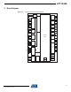
3. Package and Pinout Figure 3-1.
AT73C246 4. Pin Description Table 4-1. Pin Description Pin Name I/O Pin Number Type VBACKUP Output 1 Analog RTC supply LED Output 2 Digital Output for blinking led. Leave not connected if a LED is not wired. ANA0 Input 3 Analog Measurement input 0 ANA1 Input 4 Analog Measurement Input 1 ANA2 Input 5 Analog Measurement Input 2 ANA3 Input 6 Analog Measurement Input 3 VINSYS Input 7 Power PMU core supply VDDC Output 8 Analog PMU / Audio digital supply.
Table 4-1. Pin Name Pin Description I/O Pin Number Type MICLN Input 31 Analog Audio negative microphone input left MICRN Input 32 Analog Audio negative microphone input right MICR Input 33 Analog Audio positive microphone input right MICL Input 34 Analog Audio positive microphone input left MICBIAS Output 35 Analog Voltage bias for electret microphone VDD4 Output 36 Power LDO4 output - 3.
AT73C246 Table 4-1. Pin Description Pin Name I/O Pin Number Type Input 63 Analog RTC crystal oscillator input XOUT Output 64 Analog RTC crystal oscillator output DGND Ground 65 Analog PMU digital ground + Thermal pad.
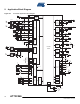
5. Application Block Diagram Figure 5-1. AT73C246 Application Block Diagram VIN4 VIN C42 10µF 37 36 VDD4 LDO4 3.3V Max: 200mA (CODEC) C41 10µF LINEJACK 100 R30 J1 C40 1nF R29 100K C38 1nF R28 100K R31 100 100 AUXJACK R26 J2 C36 1nF R25 100K C34 1nF R24 100K R27 100 3.3µF C39 BUCK0 28 1.8V LINR 3.3µF C35 AUXL 30 3.
AT73C246 Table 5-1. Typical Application Components Design Schematic Reference Value Description R1, R18, R19, R22, R23 2kΩ 5% / 0.063W R2 560kΩ 1% / 0.063W R3, R4, R6,R7 4.7kΩ 5% / 0.063W R5 470Ω 5% / 0.063W R8, R9, R10, R11, R14, R15, R26, R27, R30, R31 100Ω 5% / 0.063W R12, R13, R24, R25, R28, R29 100kΩ 5% / 0.063W C1, C3, C6, C7, C8, C10, C41, C42 10µF X5R / 6.3V TDK: C1608X5R0J106MT MURATA: GRM188R60J106ME47 C2, C4 22µF X5R / 6.
AT73C246 11050A–PMAAC–07-Apr-10
AT73C246 6. Absolute Maximum Ratings Table 6-1. Absolute Maximum Ratings Operating Temperature (Industrial).................-40 C to + 85⋅C(1) *NOTICE: Storage Temperature......................................-55°C to + 150°C Power Supply Input on VINSYS, VIN{0,1,3,4}, VPAD .. -0.3V to + 5.5V Power Supply Input on VIN2, AVDD ...................... -0.3V to + 3.6V Digital I/O Input Voltage...................................... -0.3V to + 5.
9. PMU Electrical Characteristics 9.1 Current Consumption Versus Modes Table 9-1. Current Consumption Versus Modes Symbol Parameter Comments Min Typ Max Units VIN Operating Supply Voltage VINSYS, VIN{0,1,3,4} present. 2.9 3.6 5.5 V POWERDOWN Mode. All LDOs and DCDC converters OFF. Audio OFF. RTC running. - 20 40 µA RUN Mode. All LDOs and DCDC converters running in PWM. Audio OFF. RTC running. - 7 15 mA STANDBY Mode. Default setup: DCDC0 ON in lowpower mode. LDO3 ON.
AT73C246 9.3 Digital I/Os DC Characteristics Table 9-3. VPAD Referred Digital I/Os Symbol Parameter VPAD Min Typ Max Units Operating Supply Voltage 1.75 3.6 5.5 V VIL Input Low-Level Voltage -0.3 - 0.3 x VPAD V VIH Input High-Level Voltage 0.7 x VPAD - VPAD + 0.3 V VOH Output High-Level Voltage IO max. 0.75 x VPAD - - V VOL Output Low-Level Voltage IO max - - 0.
9.4 DCDC0 and DCDC1 Unless otherwise specified: External components L=2.2μH, COUT=22μF and CIN=10μF. VIN{0,1} > VDD{0,1} + 500mV. TJ = [-40°C ; +125°C]. Table 9-5. DCDC0 and DCDC1 Electrical Characteristics Symbol Parameter Comments Min Typ Max Units VIN Operating Supply Voltage VIN0, VIN1 and VINSYS 2.9 3.6 5.5 V OFF - - 1 µA PFM operation. VDD0 = 1.85V, VDD1 = 1.2V - 40 80 µA PWM operation. VDD0 = 1.85V, VDD1 = 1.2V - 3 6.5 mA PFM operation. - - 50 mA PWM operation.
AT73C246 Table 9-5. DCDC0 and DCDC1 Electrical Characteristics Symbol Parameter Comments OCP Over-Current Protection Output current. TSTART Start-up Time From OFF to PWM operation. VDD(0,1) rising to 95% of final value. TPWM PFM to PWM Settling Time No output load. PWRFDET Power Fail Detector Threshold Accuracy Overload of the programmed threshold by 10mV / 5us min(3). -1 COUT Total Capacitive Load At VFB{0,1} pins. 8 Notes: Min Typ Max Units 1 1.4 1.8 A 5 ms 10 - µs +1 %.
9.5 LDO2 Unless otherwise specified: External components COUT=10µF, CIN=10μF, TJ = [-40°C ; +125°C]. Table 9-6. LDO2 Electrical Characteristics Symbol Parameter Comments Min Typ Max Units VIN Operating Supply Voltage VIN2 1.65 1.8 3.6 V IDD Supply Current(1) OFF - - 1 µA ON - - 250 µA IO Output Current VIN2 > VDD2 + 500mV. - - 300 mA VDD2 Default Output Voltage(2) - 1 - V VDD_RANGE Programmable Output Voltage Range 1.
AT73C246 9.6 LDO3 Unless otherwise specified: External components COUT=10µF, CIN=10μF, TJ = [-40°C ; +125°C]. Table 9-7. LDO3 Electrical Characteristics Symbol Parameter Comments Min Typ Max Units VIN Operating Supply Voltage VIN3 2.9 3.6 5.5 V IDD Supply Current(1) OFF - - 1 µA ON - - 350 µA IO Output Current VIN3 > VDD3 + 300mV. - - 200 mA VDD3 Default Output Voltage(2) - 3.3 - V VDD_RANGE Programmable Output Voltage Range 3.
9.7 LDO4 Unless otherwise specified: External components COUT=10µF, CIN=10μF, TJ = [-40°C ; +125°C]. Table 9-8. LDO4 Electrical Characteristics Symbol Parameter Comments Min Typ Max Units VIN Operating Supply Voltage VIN4 2.9 3.6 5.5 V IDD Supply Current(1) OFF - - 1 µA ON - - 350 µA IO Output Current VIN4 > VDD4 + 300mV. - - 200 mA VDD4 Default Output Voltage(2) - 3.3 - V VDD_RANGE Programmable Output Voltage Range 3.
AT73C246 9.8 LDO5 Unless otherwise specified: External components COUT=2.2µF, CIN=10μF, TJ = [-40°C ; +125°C]. Table 9-9. LDO5 Electrical Characteristics Symbol Parameter Comments Min Typ Max Units VIN Operating Supply Voltage VINSYS 2.7 3.6 5.5 V IDD Supply Current(1) OFF - - 1 µA ON - - 7 µA IO Output Current - - 10 mA VBACKUP Output Voltage Accuracy 2.42 2.5 2.58 V ΔVDD_VIN Static Line Regulation VINSYS from 2.7 to 5.
9.9 Measurement Bridge and 10-bit ADC Table 9-10. Symbol Measurement Bridge and 10-bit ADC Electrical Characteristics Parameter (1) Comments Min Typ Max Units VINSYS 2.9 3.6 5.5 V OFF - - 1 µA ON - - 2 mA 1.75 1.8 1.85 V VIN Operating Supply Voltage IDD Supply Current VREF Reference Voltage Internally connected to VDDC pin.
AT73C246 9.10 RTC Crystal Oscillator Table 9-11. RTC Crystal Oscillator Electrical Characteristics Symbol Parameter Comments Min Typ Max Units VIN Operating Supply Voltage VBACKUP 1.75 2.5 2.65 V Freq Frequency with crystal - 32.768 - kHz Duty Duty Cycle 40 50 60 % IDD Supply Current(1) OFF - - 5 nA ON - - 1.
10. Audio Codec Electrical Characteristics Unless otherwise specified: AVDD = 3.3V, TA = 25C, MCLK = 12.288MHz, FS = 48kHz. Master mode and 24-bit operation on I2S port. All gains set to 0dB, audio effects are off. Noise measurements are made in the [20Hz-20kHz] band using the A-Weighting filter. Distortion measurements are made from the 2nd to the 5th harmonic products of a 997Hz input sinewave. Input sources have an internal impedance of 50 Ohms. Audio Path without mixing capability. Table 10-1.
AT73C246 Table 10-3. Microphone Record Path: Microphone Input to ADC Output Symbol Parameter DR Dynamic Range(3) THD Total Harmonic Distortion XTALK GLINE Comments Min Typ Max Units AVDD = 3.3V 85 96 - dB AVDD = 2.7V 82 93 - dB - -84 -74 dB Left / Right Channel separation(5) 80 90 - dB Programmable Gain Range 0 - 46 dB Gain Step Size - 1 - dB 80 - - dB 8.4 12 15.
Table 10-5.
AT73C246 11. PMU Functional Description 11.1 Power Manager State Diagram Figure 11-1. AT73C246 Power Manager Functional State Diagram POWERDOWN (all supplies OFF) RSTB = 0 POWER-OFF or POWER-FAIL EVENT STANDBY-OUT or POWER-FAIL EVENT HRST_POWERDOWN EVENT POWER-ON EVENT & Vin > 3.
11.2 PMU Startup and Shutdown State Diagram Figure 11-2. AT73C246 Start-up and Shutdown State Diagram Vin > 2V VINSYS < 2.7V or VDDC_KO Start : VINSYS Monitor & VDDC = 1.8V. PMU_RSTN = 0 AUDIO_RSTN = 0 VINSYS > 2.7V & VDDC_OK PMU_RSTN = 1 AUDIO_RSTN = 1 1 1 READ CONFIG VBACKUP < 1.8V VBACKUP > 1.8V RTC_RSTN = 0 START LDO5 (BACKUP) OFF LDO5 (BACKUP) 1 START LDO5 (BACKUP) VBACKUP > 1.8V VBACKUP > 1.8V RTC_RSTN = 1 VINSYS < 2.
AT73C246 (VDDC = 1.8V) is started. During this PMU reset, the ‘LED’ pin is driven to VINSYS (LED is OFF). • When VDDC is ready and VINSYS > 2.7V, the internal reset signals previously mentioned are released, thus enabling the PMU digital core functions. • Before starting the LDO5 (RTC supply), VBACKUP voltage is monitored and if it is lower than 1.8V, the RTC function is resetted. In case of VBACKUP > 1.8V, no reset is issued on the RTC function.
11.3.6 WAKEUP EVENTS WAKEUP EVENTS are validated if one of the listed condition is true: • WAKEUP0 pin goes from low to high state and WAKEUP0 bit is set to ‘1’ (see Table 11-1) in register 0x01 (PMU_WAKEUP_EVENTS). • WAKEUP1 pin goes from low to high state and WAKEUP1 bit is set to ‘1’ (see Table 11-1) in register 0x01 (PMU_WAKEUP_EVENTS). • WAKEUP2 pin goes from low to high state and WAKEUP2 bit is set to ‘1’ (see Table 11-1) in register 0x01 (PMU_WAKEUP_EVENTS).
AT73C246 Table 11-1. EVENTS Timing Table Pin Parameter Comments Min Typ Max Units WAKEUP0 Pin pulsed to VBACKUP Level. Pulse Width. Pin used as WAKEUP event 5 - - ns WAKEUP1 Pin pulsed to VPAD Level. Pulse Width. Pin used as WAKEUP event 5 - - ns WAKEUP2 Pin pulsed to VPAD Level. Pulse Width. Pin used as WAKEUP event 5 - - ns WAKEUP3 Pin pulsed to VPAD Level. Pulse Width. Pin used as WAKEUP event 5 - - ns 11.
Figure 11-3. AT73C246 - RUN to POWERDOWN state Supplies Shutdown timing diagram. SEQUENCE A RUN STATE SEQUENCE B POWERDOWN STATE SUPPLIES SHUTDOWN RUN STATE POWERDOWN STATE SUPPLIES SHUTDOWN TPWRDOWN TPWRDOWN POWEROFF EVENT POWEROFF EVENT TOFF_AUDIO RSTB 3.3V TOFF_AUDIO RSTB TOFF_VDD3 1V VDD3 (3.3V) TOFF_VDD2 VDD2 (1V) 1.2V TOFF_VDD1 1.2V VDD1 (1.2V) TOFF_VDD1 VDD1 (1.2V) 1.85V TOFF_VDD0 TOFF_VDD0 1.85V VDD0 (1.85V) VDD0 (1.85V) 1V TOFF_VDD2 3.
AT73C246 When the POWERDOWN state is reached from the STANDBY state, the CPU power supplies are switched off sequentially as described in Figure 11-4. Figure 11-4. AT73C246 - STANDBY to POWERDOWN state Supplies Shutdown timing diagram. SEQUENCE A STANDBY STATE SEQUENCE B STANDBY STATE POWERDOWN STATE SUPPLIES SHUTDOWN TSTBY_OUT POWERDOWN STATE SUPPLIES SHUTDOWN TSTBY_OUT STANDBY_OUT EVENT STANDBY_OUT EVENT RSTB RSTB TOFF_VDD3 3.3V 1V VDD3 (3.3V) TOFF_VDD2 VDD2 (1V) 1.2V TOFF_VDD1 1.
When RUN state is reached from the POWERDOWN state, the power supplies are sequentially started-up according to the Figure 11-5 Figure 11-5. AT73C246 - POWERDOWN to RUN state Supplies Start-Up timing diagram.. SEQUENCE A POWERDOWN STATE SEQUENCE B SUPPLIES START UP RUN STATE PWREN EVENT POWERDOWN STATE SUPPLIES START UP RUN STATE PWREN EVENT TON_SYS TON_SYS 1V VDD2 (1V) 3.3V VDD3 (3.3V) TON_VDD2 TON_VDD3 1.85V VDD0 (1.85V) 1.85V VDD0 (1.85V) TON_VDD0 TON_VDD0 1.2V VDD1 (1.2V) 1.
AT73C246 When RUN state is reached from the STANDBY state, the power supplies are sequentially started-up according to the Figure 11-6. Figure 11-6. AT73C246 - STANDBY to RUN state Supplies Start-Up timing diagram. SEQUENCE A STANDBY STATE SEQUENCE B SUPPLIES START UP RUN STATE WAKEUP EVENT STANDBY STATE SUPPLIES START UP RUN STATE WAKEUP EVENT TON_SYS TON_SYS 1V VDD2 (1V) VDD3 (3.3V) TON_VDD2 3.3V VDD3 ON or OFF TON_VDD3 1.85V 1.85V VDD0 VDD0 (1.85V) PFM TON_VDD0 VDD1 (1.
Figure 11-7. AT73C246 - RUN to STANDBY state Supplies Shutdown timing diagram. SEQUENCE A RUN STATE SEQUENCE B STANDBY STATE SUPPLIES SHUTDOWN RUN STATE TSTANDBY TSTANDBY STANDBY EVENT STANDBY EVENT TWAIT + TOFF_AUDIO TOFF_VDD3 RSTB TWAIT + TOFF_AUDIO TOFF_VDD2 RSTB 3.3V 1V VDD3 (3.3V) (VDD3 ON or OFF) TOFF_VDD1 VDD2 (1V) 1.2V VDD1 VDD1 (1.2V) TPWM PWM PFM PWM TOFF_VDD0 1.85V VDD0 (1.85V) VDD1 VDD1 (1.2V) PFM PWM VDD0 VDD0 (1.85V) PFM TOFF_VDD2 TOFF_VDD0 1.85V 1.
AT73C246 Figure 11-8. AT73C246 - HRST state Supplies Shutdown timing diagram. SEQUENCE A RUN / STANDBY / POWERDOWN SEQUENCE B SUPPLIES SHUTDOWN STATE RUN / STANDBY / POWERDOWN HRST STATE HRST STATE SUPPLIES SHUTDOWN STATE THRST THRST HRST_EVENT EVENT HRST_EVENT EVENT TOFF_AUDIO TOFF_AUDIO RSTB RSTB 3.3V TOFF_VDD3 1V VDD3 (3.3V) TOFF_VDD2 VDD2 (1V) 1.2V TOFF_VDD1 TOFF_VDD1 1.2V VDD1 (1.2V) VDD1 (1.2V) 1.85V TOFF_VDD0 1.85V VDD0 (1.85V) TOFF_VDD0 VDD0 (1.
11.5 DCDC0 and DCDC1 Functional Description DCDC0 and DCDC1 are 2 identical high performance synchronous step-down (buck) converters. They feature: • 2 control modes: PFM and PWM, • A soft start circuit, • A software programmable output voltage between 0.8 and 3.6V with automatic ramping for DVS application, • An Over-Current-Protection circuit, • A 180 degree out of phase operating mode. 11.5.1 PFM and PWM Control Modes Pulse Frequency Modulation control is an hysteretic control of the output voltage.
AT73C246 11.6 LDO2 Functional Description LDO2 is a linear voltage regulator intended to supply CPU core voltages in the range 0.8V to 1.35V. Its maximum input voltage is 3.6V. Thus, it must not be wired to the VIN plane with VINSYS, VIN0, VIN1, VIN3 and VIN4 if VIN is above 3.6V. Considering its low-output voltage and for the sake of efficiency and power dissipation, the user may connect it at the output of DCDC0.
At power up, LDO3 an LDO4 default output voltages are both 3.3V. For different default output voltages, please contact Atmel. 11.8 Power Fail Detectors AT73C246 features a Power Fail detector on each CPU supplies (VDD0, VDD1, VDD2, VDD3). This function is made of a comparator that toggles each time one the listed power supplies goes below a defined threshold. The comparator toggling is considered by the PMU digital state machine as a POWER-FAIL event.
AT73C246 Figure 11-9. Measurement Bridge and 10-bit ADC Block Diagram.
11.10 Real Time Clock (RTC) User Interface Figure 11-10. RTC Block Diagram RTC DATA 3 RTC DATA 2 RTC DATA 1 RTC DATA 0 CONTROL REGISTER MODE REGISTER TIME REGISTER RTC_SEL CALENDAR REGISTER TIME ALARM REGISTER CALENDAR ALARM REGISTER RTC CTRL RTC_EN RTC STATUS REGISTER STATUS CLEAR COMMAND REGISTER INTERRUPT ENABLE REGISTER INTERRUPT DISABLE REGISTER RTC_WRITE INTERRUPT MASK REGISTER VALID ENTRY REGISTER VERSION REGISTER RESERVED REGISTER RTC ADDR Table 11-9.
AT73C246 11.10.1 RTC Register Read/Write Operation Figure 11-11. RTC Read Operation TWI ACCESS WRITE RTC_ADDR WRITE 00 @RTC_CTRL WRITE 02 @RTC_CTRL WRITE 03 @RTC_CTRL WRITE 02 @RTC_CTRL RTC_EN = 0 RTC_EN = 1 RTC_EN = 0 RTC_EN = 0 RTC_SEL = 1 RTC_SEL = 1 RTC_SEL = 1 RTC_SEL = 0 RTC_WRITE = 0 RTC_WRITE = 0 RTC_WRITE = 0 RTC_WRITE = 0 READ RTC_DATA3 READ RTC_DATA2 READ RTC_DATA1 READ RTC_DATA0 RTC_ADDR RTC_DATA RTC_EN RTC_SEL RTC_WRITE Figure 11-12.
11.10.2 RTC Control Register Name: RTC_CR Access: Read-write Address: 0x00 31 30 29 28 27 26 25 24 – – – – – – – – 23 22 21 20 19 18 17 – – – – – – 15 14 13 12 11 10 – – – – – – 16 CALEVSEL 9 8 TIMEVSEL 7 6 5 4 3 2 1 0 – – – – – – UPDCAL UPDTIM • UPDTIM: Update Request Time Register 0 = No effect. 1 = Stops the RTC time counting. Time counting consists of second, minute and hour counters.
AT73C246 11.10.3 RTC Mode Register Name: RTC_MR Access: Read-write Address: 0x04 31 30 29 28 27 26 25 24 – – – – – – – – 23 22 21 20 19 18 17 16 – – – – – – – – 15 14 13 12 11 10 9 8 – – – – – – – – 7 6 5 4 3 2 1 0 – – – – – – – HRMOD • HRMOD: 12-/24-hour Mode 0 = 24-hour mode is selected. 1 = 12-hour mode is selected. All non-significant bits read zero.
11.10.4 RTC Time Register Name: RTC_TIMR Access: Read-write Address: 0x08 31 30 29 28 27 26 25 24 – – – – – – – – 23 22 21 20 19 18 17 16 – AMPM 15 14 10 9 8 2 1 0 HOUR 13 12 – 7 11 MIN 6 5 – 4 3 SEC • SEC: Current Second The range that can be set is 0 - 59 (BCD). The lowest four bits encode the units. The higher bits encode the tens. • MIN: Current Minute The range that can be set is 0 - 59 (BCD). The lowest four bits encode the units.
AT73C246 11.10.5 RTC Calendar Register Name: RTC_CALR Access: Read-write Address: 0x0C 31 30 – – 23 22 29 28 27 21 20 19 DAY 15 14 26 25 24 18 17 16 DATE MONTH 13 12 11 10 9 8 3 2 1 0 YEAR 7 6 5 – 4 CENT • CENT: Current Century The range that can be set is 19 - 20 (BCD). The lowest four bits encode the units. The higher bits encode the tens. • YEAR: Current Year The range that can be set is 00 - 99 (BCD). The lowest four bits encode the units.
11.10.6 RTC Time Alarm Register Name: RTC_TIMALR Access: Read-write Address: 0x10 31 30 29 28 27 26 25 24 – – – – – – – – 21 20 19 18 17 16 10 9 8 2 1 0 23 22 HOUREN AMPM 15 14 HOUR 13 12 MINEN 7 11 MIN 6 5 SECEN 4 3 SEC • SEC: Second Alarm This field is the alarm field corresponding to the BCD-coded second counter. • SECEN: Second Alarm Enable 0 = The second-matching alarm is disabled. 1 = The second-matching alarm is enabled.
AT73C246 11.10.7 RTC Calendar Alarm Register Name: RTC_CALALR Access: Read-write Address: 0x14 31 30 DATEEN – 29 28 27 26 25 24 18 17 16 DATE 23 22 21 MTHEN – – 20 19 15 14 13 12 11 10 9 8 – – – – – – – – MONTH 7 6 5 4 3 2 1 0 – – – – – – – – • MONTH: Month Alarm This field is the alarm field corresponding to the BCD-coded month counter. • MTHEN: Month Alarm Enable 0 = The month-matching alarm is disabled.
11.10.8 RTC Status Register Name: RTC_SR Access: Read-only Address: 0x18 31 30 29 28 27 26 25 24 – – – – – – – – 23 22 21 20 19 18 17 16 – – – – – – – – 15 14 13 12 11 10 9 8 – – – – – – – – 7 6 5 4 3 2 1 0 – – – CALEV TIMEV SEC ALARM ACKUPD • ACKUPD: Acknowledge for Update 0 = Time and calendar registers cannot be updated. 1 = Time and calendar registers can be updated. • ALARM: Alarm Flag 0 = No alarm matching condition occurred.
AT73C246 11.10.9 RTC Status Clear Command Register Name: RTC_SCCR Access: Write-only Address: 0x1C 31 30 29 28 27 26 25 24 – – – – – – – – 23 22 21 20 19 18 17 16 – – – – – – – – 15 14 13 12 11 10 9 8 – – – – – – – – 7 6 5 4 3 2 1 0 – – – CALCLR TIMCLR SECCLR ALRCLR ACKCLR • ACKCLR: Acknowledge Clear 0 = No effect. 1 = Clears corresponding status flag in the Status Register (RTC_SR). • ALRCLR: Alarm Clear 0 = No effect.
11.10.10 RTC Interrupt Enable Register Name: RTC_IER Access: Write-only Address: 0x20 31 30 29 28 27 26 25 24 – – – – – – – – 23 22 21 20 19 18 17 16 – – – – – – – – 15 14 13 12 11 10 9 8 – – – – – – – – 7 6 5 4 3 2 1 0 – – – CALEN TIMEN SECEN ALREN ACKEN • ACKEN: Acknowledge Update Interrupt Enable 0 = No effect. 1 = The acknowledge for update interrupt is enabled. • ALREN: Alarm Interrupt Enable 0 = No effect.
AT73C246 11.10.11 RTC Interrupt Disable Register Name: RTC_IDR Access: Write-only Address: 0x24 31 30 29 28 27 26 25 24 – – – – – – – – 23 22 21 20 19 18 17 16 – – – – – – – – 15 14 13 12 11 10 9 8 – – – – – – – – 7 6 5 4 3 2 1 0 – – – CALDIS TIMDIS SECDIS ALRDIS ACKDIS • ACKDIS: Acknowledge Update Interrupt Disable 0 = No effect. 1 = The acknowledge for update interrupt is disabled. • ALRDIS: Alarm Interrupt Disable 0 = No effect.
11.10.12 RTC Interrupt Mask Register Name: RTC_IMR Access: Read-only Address: 0x28 31 30 29 28 27 26 25 24 – – – – – – – – 23 22 21 20 19 18 17 16 – – – – – – – – 15 14 13 12 11 10 9 8 – – – – – – – – 7 6 5 4 3 2 1 0 – – – CAL TIM SEC ALR ACK • ACK: Acknowledge Update Interrupt Mask 0 = The acknowledge for update interrupt is disabled. 1 = The acknowledge for update interrupt is enabled.
AT73C246 11.10.13 RTC Valid Entry Register Name: RTC_VER Access: Read-only Address: 0x2C 31 30 29 28 27 26 25 24 – – – – – – – – 23 22 21 20 19 18 17 16 – – – – – – – – 15 14 13 12 11 10 9 8 – – – – – – – – 7 6 5 4 3 2 1 0 – – – – NVCALALR NVTIMALR NVCAL NVTIM • NVTIM: Non-valid Time 0 = No invalid data has been detected in RTC_TIMR (Time Register). 1 = RTC_TIMR has contained invalid data since it was last programmed.
11.10.14 RTC Version register Name: RTC_VERSION Access: Read-only Address: 0xFC 31 30 29 28 27 26 25 24 – – – – – – – – 23 22 21 20 19 18 17 16 – – – – – 15 14 13 12 11 – – – – 7 6 5 4 MFN 10 9 8 1 0 VERSION 3 2 VERSION • VERSION Reserved. Value subject to change. No funcionality associated. This is the Atmel internal version of the macrocell. • MFN Reserved. Value subject to change. No funcionality associated. 11.
AT73C246 12. Audio Codec Functional Description 12.1 Description AT73C246 features a high quality, low power stereo audio codec with integrated headphone amplifier. The playback channel accommodates 16 to 24-bit stereo programmable format entering the digital audio interface (I2S) and delivers an internal analog audio output through a 100dB SNR Sigma Delta Stereo DAC. An output mixer allows to mix this DAC output with a line / aux or microphone input.
AUXINR LINEINR MICRN MICBIAS 2K 200K AVDD ONMICBIAS Gain Control -35 to +12dB 1dB step INRVOL MUTEINR ONLINR MICDETLEV LINESEL ONMICBIAS MICRDIFF MICRVOL MUTEMICR ONMICR VMID AGND 200K MIXLINER MIXMICR + SELFS 0 to +46dB 1dB step WL ONMIXR ONADCR ADCR ONADCL Digital Processor PATHSEL MICR MICLDIFF DAIMODE MICLN SSCMODE ONMICL MASTER 0 to +46dB 1dB step MCLKSEL MIXMICL BCLKINV MICLVOL MUTEMICL + RINBOTH ADCL ENAC ONMIXL LINBOTH ONBYPASS DACR ONDACR ONDACL
AT73C246 12.4 Audio Controller The audio controller sequences the power-up and power-down of the audio codec sub-functions (Mic.amp / ADC / DAC / …). During these transitioning phases, the controller also manages the gain steps to fade them in and out, thus providing smooth operation. Depending on the application, two modes are provided: 1.
12.4.1 12.4.1.1 Audio Codec General Recommendations VMID • VMID is the common mode voltage of the audio codec analog core. It is recommended to decouple this voltage with a 1uF capacitor to ensure low noise operation as well as slow (thus silent) transients at codec power up and power down. • The VMID capacitor is charged and discharged whenever the ENAC bit is set or cleared. Particularly, placing the audio codec in STANDBY mode does not discharge the VMID capacitor.
AT73C246 Figure 12-4. AC / DC Coupled Load Management Schematic View VIN4 AT73C246 LDO4 CL LEFT VDD4 HPL S1 10uF RL ENAC DCBLOCK.ONHP AVDD 200k VMID BUFFER VMID CR S2 RR RIGHT HPR 1uF AGND 200k Figure 12-5. Audio Codec Typical Startup and Shutdown Waveforms With AC Coupled Loads. VDD4 VMID HP(L/R) DCBLOCK ENAC STANDBY S1 & S2 S1 AND S2 OPENED BY AUDIO CODEC 12.4.1.3 MUTE Register By default, the audio codec starts muted.
500ms timeout. Contrary to the first point, which has no timeout, the audio power-off time limit is here fixed to 500ms. Beyond this limit, the codec is hardly reseted as in the following point. • PMU Power-fail event. In this case, the PMU finite state machine makes an immediate hard reset of the audio codec to ensure fast shutdown. This case may generate an audible click / pop noise. 12.4.1.
AT73C246 master clock must be running to properly shutdown the codec. This time linearly varies with ASR_TIME value. See Table 12-1 Table 12-1. ASR_TIME Audio Codec Maximum Power-off Time Power-off time (ms) 00 375 01 750 10 1500 11 3000 The analog power-off time corresponds to the VMID’s discharge time specified in “Audio Codec Bias” on page 22: TMID_OFF.
12.4.2.2 Pause Management With STANDBY Bit To pause the audio codec activity and reduce power consumption to few hundreds of microamps, the STANDBY bit can be activated in register AUTOSTART (0x10). The Audio codec will then: • Softly ramp down all the path concerned gains down-to mute and • Power off all the audio sub-functions. The registers INPUT_CONTROL (0x1E), OUTPUT_CONTROL (0x1F), and INPUT_MIXER (0x20) are modified by the audio controller. Notes: 1.
AT73C246 • INPUT_CONTROL (0x1E) • OUTPUT_CONTROL (0x1F) • INPUT_MIXER (0x20) Like in the automatic path configuration, the audio controller will sequence audio codec subfunctions ON/OFF as well as gain stepping. However, the audio path is no more selected via the "PATHSEL" value in register AUTOSTART. To specify a custom audio path: • The bit CUSTCONF in register AUDIO_CONTROL (0x11) must be set to '1' to specify the 'custom' path configuration mode.
• Current consumptions don’t account for load consumption and are measured in AVDD pin and VINSYS pin. Table 12-2. Audio PATH Power Consumption PATH_SEL AUDIO PATH Description Consumption Units VINSYS AVDD 0.10 0.61 mA 00000 No Path 00001 DAC Playback Digital IN - Headphone OUT 1.80 5.2 mA 00010 Mic Sidetone Microphone IN - Headphone OUT 0.10 2.65 mA 00011 Aux Bypass Aux IN - Headphone OUT 0.10 2.65 mA 00100 Line Bypass Line IN - Headphone OUT 0.10 2.
AT73C246 Table 12-2. Audio PATH Power Consumption PATH_SEL AUDIO PATH Description Consumption VINSYS AVDD Units 10111 DAC Playback + Line Bypass and Line Record Digital + Line IN - Headphone OUT Line IN - Digital OUT 3.80 8.00 mA 11000 DAC Playback + Mic Sidetone + Aux Bypass and Mic + Aux Record Digital + Mic + Aux IN - Headphone OUT Mic + Aux IN - Digital OUT 3.80 8.
12.6 12.6.1 Digital Audio Interface General Description AT73C246 features a 16 to 24-bit multi-mode master / slave I2S port. The following modes are provided: • I2S, • Left Justified, • Right Justified, and • SSC The I2S port is configured through register I2S_CONTROL (0x13) and FRAME_CONTROL (0x14). For each of the listed modes, the data transfer is described in the following sections. The following table provides authorized MCLK / FS ratios and associated filter types: Table 12-3. 12 MHz(1) 12.
AT73C246 12.6.3 Data Transfer: Left Justified Mode Figure 12-8. N-bit Left Justified Mode (FS = 44.1KHz - MCLK = 256 x FS) MCLK LRFS BCLK SDOUT SDIN Ln Ln-1 Ln-2 L0 Rn R n-1 R n-2 n bits Left Channel 12.6.4 R3 R2 R1 R0 n bits Right Channel Data Transfer: Right Justified Mode Figure 12-9. N-bit Right Justified Mode (FS = 44.
12.6.5 Timing Specifications Figure 12-10. Timing Diagram of data interface (I²S Mode) TLRCLK TLRCLK VIH LRFS VIL TBCLK VIH BCLK VIL THSDX TLSDX DAI DAO VXH LSB VXL Word N-1 Right Channel Table 12-4.
AT73C246 Figure 12-12. DAC Type 1 Frequency Response Overall Ripple Figure 12-13. DAC Type 2 Frequency Response Overall Ripple Figure 12-14.
Figure 12-15. DAC Type 4 Frequency Response Overall 12.7.2 Ripple ADC Frequency Response The following diagrams are referred to FS = 1 (Sampling Frequency). Figure 12-16. ADC Type 0 Frequency Response Overall Ripple Figure 12-17.
AT73C246 Figure 12-18. ADC Type 2 Frequency Response Overall Ripple Figure 12-19. ADC Type 3 Frequency Response Overall Ripple Figure 12-20.
12.7.3 12.7.3.1 De-Emphasis Filter Frequency Response De-Emphasis Filter: Frequency Response & Error (FS = 32kHz) Figure 12-21. De-Emphasis Filter: Frequency Response & Error (FS = 32kHz) Error Response (dB) Response (dB) Response Fequency (Hz) 12.7.3.2 Fequency (Hz) De-Emphasis Filter: Frequency Response & Error (FS = 44.1kHz) Figure 12-22. De-Emphasis Filter: Frequency Response & Error (FS = 44.1kHz) Error Response (dB) Response (dB) Response Fequency (Hz) 12.7.3.
AT73C246 12.7.4 Equalizer Frequency Response The following figures show the frequency response of the equalizer function implemented in the D/A channels. Figure 12-24. Bass Filters Response dB Fs Figure 12-25.
Figure 12-26. Treble Filters Response dB Fs 12.8 12.8.
AT73C246 Figure 12-27. Mono - Single Ended and Differential Microphone Applications VIN4 VIN4 LDO4 LDO4 VDD4 VDD4 10uF AVDD 10uF AVDD 2k 2k MICBIAS MICBIAS AT73C246 2k MICL AT73C246 10uF 1uF 1k MICL M 2.2nF M 1uF MICLN NC MICR NC MICR NC MICRN NC MICRN NC MICLN 10uF 1uF 1k 2.2nF Figure 12-28.
12.8.2 Aux / Line Inputs Figure 12-30. Aux and Line Input Application Circuits 3.3uF 100 AUXL 10nF ON-BOARD AUDIO IC SOURCE (FM receiver, ...) 10nF AUXR 100 3.3uF AT73C246 3.3uF 100 10nF 100k 10nF 100k LINL jack LINR 100 3.3uF 12.8.3 Line / Headphone Outputs Figure 12-31. AC Coupled Output Application Circuits 3.3uF 330uF 100 100k HPR 100k HPR jack HPVCM jack AT73C246 NC HPVCM NC 3.
AT73C246 13. Two Wire Interface and Control Registers 13.1 Two-wire Interface (TWI) Protocol The two-wire interface interconnects components on a unique two-wire bus, made up of one clock line and one data line with speeds up to 400 Kbits per second, based one a byte oriented transfer format. The TWI is slave only and single byte access. The interface adds flexibility to the power supply solution, enabling LDO regulators to be controlled depending on the instantaneous application requirements.
For a read operation a repeated Start condition needs to be generated followed by a read on the device. Figure 13-3. TWD Write Operation S TWD ADDR W A IADDR DATA A A P Figure 13-4.
AT73C246 13.2 13.2.1 PMU Register Tables Register Mapping Table 13-1.
Table 13-1.
AT73C246 13.2.2 PMU Control Name: PMU_MODES Access: Read / Write Address: 0x00 7 6 5 4 3 2 1 0 - - - - - STANDBY PWRDOWN RUN Table 13-2. PMU_MODES (0x00) Structure Bit Name Description Reset value 7:3 - unused 00000 STANDBY STANDBY request 0: Default value. 1: STANDBY request. Reset to 0 at STANDBY exit. 0 1 PWRDOWN POWERDOWN request 0: Default value. 1: POWERDOWN request. Reset to 0 when POWERDOWN state reached. 0 0 RUN RUN mode 0 2 Notes: 1.
Name: PMU_WAKEUP_EVENTS Access: Read / Write Address: 0x01 7 6 5 4 3 2 1 0 - - RTC PWREN WAKEUP3 WAKEUP2 WAKEUP1 WAKEUP0 Table 13-3.
AT73C246 Name: PMU_WAKEUP_TRIG Access: Read Only Address: 0x02 7 6 5 4 3 2 1 0 - - RTCR PWREN WAKEUP3 WAKEUP2 WAKEUP1 WAKEUP0 Table 13-4.
Name: PMU_STANDBY_SUPPLIES Access: Read / Write Address: 0x03 7 6 5 4 3 2 1 0 - - LP_VDD1 LP_VDD0 VDD3 VDD2 VDD1 VDD0 Table 13-5.
AT73C246 Name: PMU_SUPPLY_CTRL Access: Read / Write Address: 0x04 7 6 5 4 3 2 1 0 - - IN_PHASE DVS_VDD4 DVS_VDD3 DVS_VDD2 DVS_VDD1 DVS_VDD0 Table 13-6.
Name: PMU_RST_LVL Access: Read / Write Address: 0x05 7 6 RST_VDD3 Table 13-7. 4 RST_VDD2 3 2 RST_VDD1 1 0 RST_VDD0 PMU_RST_LVL (0x05) Structure Bit Name Description Reset value 7:6 RST_VDD3 RST level on VDD3 01 5:4 RST_VDD2 RST level on VDD2 10 3:2 RST_VDD1 RST level on VDD1 10 1:0 RST_VDD0 RST level on VDD0 11 Table 13-8. 86 5 VDDx Reset Level Selection Table RST_VDDx RST LEVEL 00 0.85 x VDDx 01 0.90 x VDDx 10 0.92 x VDDx 11 0.
AT73C246 Name: VDD0_CTRL Access: Read / Write Address: 0x06 7 6 ON_VDD0 LPMODE Table 13-9. 5 4 3 2 1 0 VDD0_SEL VDD0_CTRL (0x06) Structure Bit Name Description Reset value 7 ON_VDD0 VDD0 ON/OFF 0: OFF 1: ON 0 6 LPMODE VDD0 Low power mode 0: Full power (PWM) 1: Low power (PFM) 0 5:0 VDD0_SEL VDD0 voltage selection 010101 Table 13-10. VDD0 Voltage Selection Table VDD0_SEL VDD0 (V) VDD0_SEL VDD0 (V) VDD0_SEL VDD0 (V) 000000 0.80 010011 1.75 100110 2.70 000001 0.
Name: VDD1_CTRL Access: Read / Write Address: 0x07 7 6 5 ON_VDD1 LPMODE 4 3 2 1 0 VDD1_SEL Table 13-11. VDD1_CTRL (0x07) Structure Bit Name Description Reset value 7 ON_VDD1 VDD1 ON / OFF 0: OFF 1: ON 0 6 LPMODE VDD1 Low power mode 0: Full power (PWM) 1: Low power (PFM) 0 5:0 VDD1_SEL VDD1 voltage selection 001000 Table 13-12. VDD1 Voltage Selection Table 88 VDD1_SEL VDD1 (V) VDD1_SEL VDD1 (V) VDD1_SEL VDD1 (V) 000000 0.80 010011 1.75 100110 2.70 000001 0.
AT73C246 Name: VDD2_CTRL Access: Read / Write Address: 0x08 7 6 5 ON_VDD2 - - 4 3 2 1 0 VDD2_SEL Table 13-13. VDD2_CTRL (0x08) Structure Bit Name Description Reset value 7 ON_VDD2 VDD2 ON / OFF 0: OFF 1: ON 0 6:5 - unused 00 4:0 VDD2_SEL VDD2 voltage selection 00100 Table 13-14. VDD2 Voltage Selection Table VDD2_SEL VDD2 (V) 00000 0.80 00001 0.85 00010 0.90 00011 0.95 00100 1.00 00101 1.05 00110 1.10 00111 1.15 01000 1.20 01001 1.25 01010 1.
Name: VDD3_CTRL Access: Read / Write Address: 0x09 7 6 5 ON_VDD3 - - 4 3 2 1 0 VDD3_SEL Table 13-15. VDD3_CTRL (0x09) Structure Bit Name Description Reset value 7 ON_VDD3 VDD3 ON / OFF 0: OFF 1: ON 0 6:5 - unused 00 4:0 VDD3_SEL VDD3 voltage selection 01100 Table 13-16. VDD3 Voltage Selection Table 90 VDD3_SEL VDD3 (V) 00000 2.70 00001 2.75 00010 2.80 00011 2.85 00100 2.90 00101 2.95 00110 3.00 00111 3.05 01000 3.10 01001 3.15 01010 3.20 01011 3.
AT73C246 Name: VDD4_CTRL Access: Read / Write Address: 0x0A 7 6 5 ON_VDD4 - - 4 3 2 1 0 VDD4_SEL Table 13-17. VDD4_CTRL (0x0A) Structure Bit Name Description Reset value 7 ON_VDD4 VDD4 ON / OFF 0: OFF 1: ON 0 6:5 - unused 00 4:0 VDD4_SEL VDD4 voltage selection 01100 Table 13-18. VDD4 Voltage Selection Table VDD4_SEL VDD4 (V) 00000 2.70 00001 2.75 00010 2.80 00011 2.85 00100 2.90 00101 2.95 00110 3.00 00111 3.05 01000 3.10 01001 3.15 01010 3.
Name: PMU_LED Access: Read / Write Address: 0x0B 7 6 5 4 3 TON_LED 2 PERIOD_LED 1 0 BLINK ON_LED Table 13-19. PMU_LED (0x0B) Structure Bit Name Description Reset value 7:5 TON_LED LED ‘ON’ time 000 4:2 PERIOD_LED LED blinking period 010 1 BLINK Blinking function ON / OFF 0: OFF 1: ON 0 0 ON_LED Led ON / OFF 0: OFF 1: ON 0 Table 13-20. LED Blinking Function Parameters Selection Table TON_LED LED ‘ON’ Time (ms) PERIOD_LED BLINKING PERIOD (s) 000 25 000 0.
AT73C246 Name: PMU_MASK Access: Read / Write Address: 0x0C 7 6 5 4 3 2 1 0 - - - - - - RTC_ALA RM RTC_IT Table 13-21. PMU_MASK (0x0C) Structure Bit Name Description Reset value 7:2 - unused 111111 1 RTC_ALARM Mask RTC alarm 0: not masked 1: masked 1 0 RTC_IT Mask RTC interrupt 0: not masked 1: masked 1 Name: PMU_IT Access: Read Only Address: 0x0D 7 6 5 4 3 2 1 0 - - - - - - RTC_ALA RM RTC_IT Table 13-22.
Name: PMU_WAKEUP_SUPPLIES Access: Read / Write Address: 0x0E 7 6 5 4 3 2 1 0 - - - - VDD0_WUP VDD1_WUP VDD2_WUP VDD3_WUP Table 13-23.
AT73C246 Name: AUTOSTART Access: Read / Write Address: 0x10 7 6 5 4 - ENAC STANDBY 3 2 1 0 PATH_SEL Table 13-24. AUTOSTART (0x10) Structure Bit Name Description Reset value 7 - unused 0 6 ENAC Audio Codec ON / OFF 0: OFF 1: ON 0 5 STANDBY Audio STANDBY mode ON / OFF 0: Audio codec active 1: Audio codec in standby 1 4:0 PATH_SEL Audio PATH selection 00000 Table 13-25.
Table 13-25.
AT73C246 Name: AUDIO_CONTROL Access: Read / Write Address: 0x11 7 6 5 4 3 2 - BCLKINV DCBLOCK ENCONF CUST_CO NF ENASR 1 0 ASR_TIME Table 13-26. AUDIO_CONTROL (0x11) Structure Bit Name Description Reset value 7 - - 0 6 BLCKINV Bit clock inversion on I2S port 0: not inverted 1: inverted 0 5 DCBLOCK Headphone output coupling configuration 0: DC coupled (capless operation) 1: AC coupled 0 4 ENCONF Custom configuration enable 0: Default value.
Name: MIC_CONTROL Access: Read / Write Address: 0x12 7 6 5 4 - - MICLDIFF MICRDIFF 3 2 MICDET 1 0 ONMICBIAS MICDET_ST Table 13-28.
AT73C246 Name: DAI_CONTROL Access: Read / Write Address: 0x13 7 6 5 4 3 - - - - MASTER 2 1 0 MCLKSEL Table 13-30. DAI_CONTROL (0x13) Structure Bit Name Description Reset value 7:4 - unused 0000 3 MASTER(1) MASTER / SLAVE operation on DAI port 0: Slave 1: Master 0 2:0 MCLKSEL Audio Master clock frequency selection 001 Note: 1. The MASTER mode is not provided for 12.0000 MHz clock case and Right-Justified mode on DAI. Table 13-31.
Name: FRAME_CONTROL Access: Read / Write Address: 0x14 7 6 SSCMODE 5 4 WL 3 2 DAI_MODE 1 0 SELFS Table 13-32. FRAME_CONTROL (0x14) Structure Bit Name Description Reset value 7 SSCMODE SSC mode for DAI 0: DAI according to DAI_MODE bits 1: SSC mode 0 6:5 WL Word length selection 11 4:3 DAI_MODE Digital Audio Interface mode control 00 2:0 SELFS Audio Frame frequency selection 011 Table 13-33.
AT73C246 Name: MUTE Access: Read / Write Address: 0x15 7 6 5 4 3 2 1 0 MUTEDACL MUTEDAC R MUTEINL MUTEINR MUTEMICL MUTEMICR MUTEHPL MUTEHPR Table 13-36.
Name: MICLVOL Access: Read / Write Address: 0x16 7 6 - - 5 4 3 2 1 0 MICLVOL Table 13-37. MICLVOL (0x16) Structure Bit Name Description Reset value 7:6 - unused 00 5:0 MICLVOL Microphone Left volume selection 000000 Table 13-38.
AT73C246 Name: MICRVOL Access: Read / Write Address: 0x17 7 6 - - 5 4 3 2 1 0 MICRVOL Table 13-39. MICRVOL (0x17) Structure Bit Name Description Reset value 7:6 - unused 0 5:0 MICRVOL Microphone Right volume selection 000000 Table 13-40.
Name: INLVOL Access: Read / Write Address: 0x18 7 6 5 4 INLBOTH 3 2 1 0 INLVOL Table 13-41. INLVOL (0x18) Structure Bit Name Description Reset value 7 INLBOTH AUX / LINE Left volume controls Right channel 0: inactive 1: active. Prioritary bit over INRBOTH. 1 6:0 INLVOL AUX / LINE input Left volume selection 0000000 Table 13-42.
AT73C246 Name: INRVOL Access: Read / Write Address: 0x19 7 6 5 4 INRBOTH 3 2 1 0 INRVOL Table 13-43. INRVOL (0x19) Structure Bit Name Description Reset value 7 INRBOTH AUX / LINE Right volume controls left channel 0: inactive 1: active. 0 6:0 INRVOL AUX / LINE input Right volume selection 0000000 Table 13-44.
Name: HPLVOL Access: Read / Write Address: 0x1A 7 6 5 4 3 2 1 0 HPLVOL Table 13-45. HPLVOL (0x1A) Structure Bit Name Description Reset value 7:0 HPLVOL Headphone Left volume selection 00000000 Table 13-46.
AT73C246 Name: HPRVOL Access: Read / Write Address: 0x1B 7 6 5 4 3 2 1 0 HPRVOL Table 13-47. HPRVOL (0x1B) Structure Bit Name Description Reset value 7:0 HPRVOL HEADSET Right volume selection 00000000 Table 13-48.
Name: HP_CONTROL Access: Read / Write Address: 0x1C 7 6 5 4 3 2 1 0 - - - - - HPDET_ST LHPBOTH RHPBOTH Table 13-49. HP_CONTROL (0x1C) Structure 108 Bit Name Description Reset value 7:3 - unused 00000 2 HPDET_ST Headphone plug in-out detector 0: OFF 1: ON 0 1 LHPBOTH Right Headphone volume follows left 0: inactive 1: active. Prioritary bit over RHPBOTH.
AT73C246 Name: AUDIO_EFFECTS Access: Read / Write Address: 0x1D 7 6 3DFX_DEPTH 5 4 ON3DFX SWAP_DAC 3 2 1 0 SWAP_ADC MONO_DAC MONO_ADC ONDEEMP Table 13-50.
Name: INPUT_CONTROL Access: Read / Write. This register is modified by Audio Controller at audio path change. Address: 0x1E 7 6 5 4 3 2 1 0 - LINESEL ONMICL ONMICR ONADCL ONADCR ONLINL ONLINR Table 13-52.
AT73C246 Name: OUTPUT_CONTROL Access: Read / Write This register is modified by Audio Controller at audio path change. Address: 0x1F 7 6 5 4 3 2 1 0 - ONSIDETONE ONPLAYBACK ONBYPASS ONHPL ONHPR ONDACL ONDACR Table 13-53.
Name: INPUT_MIXER Access: Read / Write This register is modified by Audio Controller at audio path change. Address: 0x20 7 6 5 4 3 2 1 0 - - MIXMICL MIXMICR MIXLINEL MIXLINER ONMIXL ONMIXR Table 13-54.
AT73C246 Name: SIDETONE_VOL Access: Read / Write Address: 0x21 7 6 5 - - - 4 3 2 1 0 SIDETONE_VOL Table 13-55. SIDETONE_VOL (0x21) Structure Bit Name 7:5 4:0 SIDETONE_VOL Description Reset value unused 000 Left / Right sidetone path attenuation 01011 Table 13-56.
Name: EQUALIZER Access: Read / Write Address: 0x22 7 6 5 4 - - - - 3 2 1 0 EQ_SEL Table 13-57. EQUALIZER (0x22) Structure Bit Name Description 7:4 3:0 Reset value 0 EQ_SEL Equalizer selection 0000 Table 13-58.
AT73C246 Name: ADC_CTRL Access: Read / Write Address: 0x30 7 6 5 4 3 ON_ADC ON_BUF - - - 2 1 0 TS Table 13-59. ADC_CTRL (0x30) Structure Bit Name Description Reset value 7 ON_ADC ADC function 0: OFF 1: ON 0 6 ON_BUF Analog buffer 0: OFF 1: ON 0 5:3 unused - 000 2:0 TS Sampling period 000 Table 13-60. ADC Sampling Period Selection Table TS SAMPLING PERIOD (s) 000 0.01 001 0.02 010 0.
Name: ADC_MUX_1 Access: Read / Write Address: 0x31 7 6 5 4 3 2 1 0 - VIN - VDD4 VDD3 VDD2 VDD1 VDD0 Table 13-61.
AT73C246 Name: ADC_MUX_2 Access: Read / Write Address: 0x32 7 6 5 4 3 2 1 0 - - - - ANA3 ANA2 ANA1 ANA0 Table 13-62.
Name: ADC_ANA0_MSB Access: Read Only Address: 0x33 7 6 5 4 3 2 1 0 ADC<9:2> Table 13-63. ADC_ANA0_MSB (0x33) Structure Bit Name Description Reset value 7:0 ADC<9:2> ADC_OUT<9:2> for ANA0 Channel 00000000 Name: ADC_ANA0_LSB Access: Read Only Address: 0x34 7 6 5 4 3 2 1 0 ADC<1:0> Table 13-64.
AT73C246 Name: ADC_ANA1_MSB Access: Read Only Address: 0x35 7 6 5 4 3 2 1 0 ADC<9:2> Table 13-65. ADC_ANA1_MSB (0x35) Structure Bit Name Description Reset value 7:0 ADC<9:2> ADC_OUT<9:2> for ANA1 Channel 00000000 Name: ADC_ANA1_LSB Access: Read Only Address: 0x36 7 6 5 4 3 2 1 0 ADC<1:0> Table 13-66.
Name: ADC_ANA2_MSB Access: Read Only Address: 0x37 7 6 5 4 3 2 1 0 ADC<9:2> Table 13-67. ADC_ANA2_MSB (0x37) Structure Bit Name Description Reset value 7:0 ADC<9:2> ADC_OUT<9:2> for ANA2 Channel 00000000 Name: ADC_ANA2_LSB Access: Read Only Address: 0x38 7 6 5 4 3 2 1 0 ADC<1:0> Table 13-68.
AT73C246 Name: ADC_ANA3_MSB Access: Read Only Address: 0x39 7 6 5 4 3 2 1 0 ADC<9:2> Table 13-69. ADC_ANA3_MSB (0x39) Structure Bit Name Description Reset value 7:0 ADC<9:2> ADC_OUT<9:2> for ANA3 Channel 00000000 Name: ADC_ANA3_LSB Access: Read Only Address: 0x3A 7 6 5 4 3 2 1 0 ADC<1:0> Table 13-70.
Name: ADC_VDD0_MSB Access: Read Only Address: 0x3B 7 6 5 4 3 2 1 0 ADC<9:2> Table 13-71. ADC_VDD0_MSB (0x3B) Structure Bit Name Description Reset value 7:0 ADC<9:2> ADC_OUT<9:2> for VDD0 Channel 00000000 Name: ADC_VDD0_LSB Access: Read Only Address: 0x3C 7 6 5 4 3 2 1 0 ADC<1:0> Table 13-72.
AT73C246 Name: ADC_VDD1_MSB Access: Read Only Address: 0x3D 7 6 5 4 3 2 1 0 ADC<9:2> Table 13-73. ADC_VDD1_MSB (0x3D) Structure Bit Name Description Reset value 7:0 ADC<9:2> ADC_OUT<9:2> for VDD1 Channel 00000000 Name: ADC_VDD1_LSB Access: Read Only Address: 0x3E 7 6 5 4 3 2 1 0 ADC<1:0> Table 13-74.
Name: ADC_VDD2_MSB Access: Read Only Address: 0x3F 7 6 5 4 3 2 1 0 ADC<9:2> Table 13-75. ADC_VDD2_MSB (0x3F) Structure Bit Name Description Reset value 7:0 ADC<9:2> ADC_OUT<9:2> for VDD2 Channel 00000000 Name: ADC_VDD2_LSB Access: Read Only Address: 0x40 7 6 5 4 3 2 1 0 ADC<1:0> Table 13-76.
AT73C246 Name: ADC_VDD3_MSB Access: Read Only Address: 0x41 7 6 5 4 3 2 1 0 ADC<9:2> Table 13-77. ADC_VDD3_MSB (0x41) Structure Bit Name Description Reset value 7:2 ADC<9:2> ADC_OUT<9:2> for VDD3 Channel 00000000 Name: ADC_VDD3_LSB Access: Read Only Address: 0x42 7 6 5 4 3 2 1 0 ADC<1:0> Table 13-78.
Name: ADC_VDD4_MSB Access: Read Only Address: 0x43 7 6 5 4 3 2 1 0 ADC<9:2> Table 13-79. ADC_VDD4_MSB (0x43) Structure Bit Name Description Reset value 7:0 ADC<9:2> ADC_OUT<9:2> for VDD4 Channel 00000000 Name: ADC_VDD4_LSB Access: Read Only Address: 0x44 7 6 5 4 3 2 1 0 ADC<1:0> Table 13-80.
AT73C246 Name: ADC_VIN_MSB Access: Read Only Address: 0x47 7 6 5 4 3 2 1 0 ADC<9:2> Table 13-81. ADC_VIN_MSB (0x47) Structure Bit Name Description Reset value 7:0 ADC<9:2> ADC_OUT<9:2> for VIN Channel 00000000 Name: ADC_VIN_LSB Access: Read Only Address: 0x48 7 6 5 4 3 2 1 0 ADC<1:0> Table 13-82.
Name: ADC_ANA_LSB Access: Read Only Address: 0x49 7 6 ADC_ANA3<1:0> 5 4 ADC_ANA2<1:0> 3 2 ADC_ANA1<1:0> 1 0 ADC_ANA0<1:0> Table 13-83.
AT73C246 Name: RTC_ADDR Access: Read / Write Address: 0x51 7 6 5 4 3 2 1 0 RTC_ADDR Table 13-85. RTC_ADDR (0x51) Structure Bit Name Description Reset value 7:0 RTC_ADDR RTC address 0000 Name: RTC_DATA0 Access: Read / Write Address: 0x52 7 6 5 4 3 2 1 0 RTC_DATA0 Table 13-86.
Name: RTC_DATA1 Access: Read / Write Address: 0x53 7 6 5 4 3 2 1 0 RTC_DATA1 Table 13-87. RTC_DATA1 (0x53) Structure Bit Name Description Reset value 7:0 RTC_DATA1 RTC DATA 1 0000000 Name: RTC_DATA2 Access: Read / Write Address: 0x54 7 6 5 4 3 2 1 0 RTC_DATA2 Table 13-88.
AT73C246 Name: BACKUP_CTRL Access: Read / Write Address: 0x56 7 6 5 4 3 2 1 0 - - - - OSC_UPDT OSC_EN OSC_STAT RST_BKUP Table 13-90. BACKUP_CTRL (0x56) Structure Bit Name Description Reset value 7:4 - unused 0000 3 OSC_UPDT RTC Oscillator update 0: No action. 1: Update RTC oscillator with OSC_EN 0 2 OSC_EN RTC Oscillator enable request 0: Oscillator off. 1: Oscillator on. 0 1 OSC_STAT RTC Oscillator status (read only) 0: Oscillator off. 1: Oscillator on.
14. PMU and Audio Soft Control: Quick Start 14.1 14.1.1 RTC Examples RTC Oscillator POWER-ON // Set OSC_EN = 1 and OSC_UPDT = 1 TWI_WRITE 0x0C @BACKUP_CTRL // Wait > 200us. WAIT 200us // Set OSC_UPDT = 0 TWI_WRITE 0x04 @BACKUP_CTRL // Read BACKUP_CTRL to verify OSC_STAT bit. Result = 0x06. TWI_READ @BACKUP_CTRL 14.1.
AT73C246 TWI_WRITE DATA2 @RTC_DATA2 TWI_WRITE DATA3 @RTC_DATA3 // Set RTC_WRITE = 1 (write) and RTC_SEL = 1 TWI_WRITE 0x06 @ RTC_CTRL // Pulse RTC_EN TWI_WRITE 0x07 @ RTC_CTRL TWI_WRITE 0x06 @ RTC_CTRL // Disable RTC access TWI_WRITE 0x00 @ RTC_CTRL 14.1.5 RTC Read Operation The following example makes a generic 32-bit read operation into the RTC macro. The 32-bit RTC data is split into 4 bytes, that are successively read over the TWI. // Select RTC_ADDR = ADDR.
// Write Time @RTC_TIMR (RTC_ADDR = 0x08) (08h 49min 59s) WRITE_RTC 0x00084959 @RTC_TIMR // Start RTC @RTC_CR (RTC_ADDR = 0x00) WRITE_RTC 0x00000000 @RTC_CR 14.2 14.2.1 Audio Examples Basic Audio Codec Setting Using Automatic Path Control The following example demonstrates an automatic audio path setting.
AT73C246 // Wait (3.tau) = 300ms with 1uF before standby release. (VMID will be // discharged only when ENAC = 0.) // From this point Audio Data can be sent over the Digital audio interface. TWI_WRITE 0x61 @ AUTOSTART. WAIT 300ms // Release standby. The audio codec starts silently, the gains are slowly // ramped up from mute to the register gains. The codec is active. TWI_WRITE 0x41 @ AUTOSTART // Codec Pause by Standby // All gains are softly ramped down to mute. The codec functions are // shut down.
// Start LDO4 @3.3V TWI_WRITE 0x8C @ VDD4_CTRL // Digital Audio Interface configuration // Master clock = 12.288MHz, Master / Slave = slave. // DAI mode = I2S mode, Word length = 24 bits, FS = 48kHz TWI_WRITE 0x01 @ DAI_CONTROL TWI_WRITE 0x63 @ FRAME_CONTROL // Analog interface configuration // Mic. config: L & R single ended, Micbias = OFF, Mic. detection = OFF.
AT73C246 // account. TWI_WRITE 0x3F @ AUDIO_CONTROL TWI_WRITE 0x2F @ AUDIO_CONTROL // STANDBY release. The codec softly starts. TWI_WRITE 0x40 @ AUTOSTART. // Codec Pause by Standby // All gains are softly ramped down to mute. The codec functions are // shut down. Current consumption is reduced to a few hundreds of micro// amps. VMID remains charged TWI_WRITE 0x60 @ AUTOSTART // Pause out: Standby release. The codec softly re-starts.
AT73C246 11050A–PMAAC–07-Apr-10
AT73C246 15. Typical Performance Characteristics 15.1 PMU: Power Supply Sequences Figure 15-1. Powerdown State to Run State Supplies Start-Up Powerdown to Run State SEQUENCE A Powerdown to Run State SEQUENCE B Figure 15-2.
Figure 15-3. Detailed Supplies Start-Up Detailed Supplies Start-Up SEQUENCE A Detailed Supplies Start-Up SEQUENCE B Figure 15-4.
AT73C246 Figure 15-5. Run State to Standby State Run To Standby State (default setting) SEQUENCE A Run To Standby State (default setting) SEQUENCE B Figure 15-6.
15.2 DCDC0 and DCDC1 Unless otherwise noted, the reported measurement were performed at room temperature. External components are those described in Section 5. “Application Block Diagram” on page 8. Figure 15-7. DCDC0 Transient Load Regulation Performance 142 DCDC0 - VIN = 3.3V - VOUT = 1.85V Load Step 0 To 600mA / 1us DCDC0 - VIN = 3.3V - VOUT = 1.85V Load Step 600 To 0mA / 1us DCDC0 - VIN = 5.5V - VOUT = 1.85V Load Step 0 To 600mA / 1us DCDC0 - VIN = 5.5V - VOUT = 1.
AT73C246 Figure 15-8. DCDC0 Ripple and Efficency Performance DCDC0 - VOUT = 1.8V Efficiency in PFM and PWM modes DCDC0 - VIN = 5.5V - VOUT = 1.
Figure 15-9. DCDC1Transient Load Regulation Performance 144 DCDC0 - VIN = 3.3V - VOUT = 1.2V Load Step 0 To 600mA / 1us DCDC0 - VIN = 3.3V - VOUT = 1.2V Load Step 600 To 0mA / 1us DCDC0 - VIN = 5.5V - VOUT = 1.2V Load Step 0 To 600mA / 1us DCDC0 - VIN = 5.5V - VOUT = 1.
AT73C246 Figure 15-10. DCDC0 Ripple and Efficiency Performance DCDC1 - VOUT = 1.2V Efficiency in PFM and PWM modes DCDC1 - VIN = 5.5V - VOUT = 1.
15.3 LDO2 Unless otherwise noted, the reported measurement were performed at room temperature. External components are those described in Section 5. “Application Block Diagram” on page 8. Figure 15-11. LDO2 Tansient and Static Load Regulation Performance 146 LDO2- VIN = 1.8V - VOUT = 1V Load Step 0 To 300mA / 1us LDO2 - VIN = 1.8V - VOUT = 1V Load Step 300 To 0mA / 1us LDO2 - VIN = 1.8V - VOUT = 1V Static Load Regulation - 0 To 300mA LDO2 - VIN = 1.7V - VOUT = 1.
AT73C246 15.4 LDO3 Unless otherwise noted, the reported measurement were performed at room temperature. External components are those described in Section 5. “Application Block Diagram” on page 8. Figure 15-12. LDO3 Transient and Static Load Regulation Performance LDO3- VIN = 5.5V - VDD3 = 3.3V Load Step 0 To 200mA / 1us LDO3 - VIN = 3.6V - VDD3 = 3.3V Static Load Regulation - 0 To 200mA LDO3 - VIN = 5.5V - VDD3 = 3.3V Load Step 200 To 0mA / 1us LDO3 - VDD3 = 3.
15.5 AUDIO Unless otherwise noted, the reported measurement were performed at room temperature with AVDD = 3.3V supplied from LDO4. Typical components as described in Section 5. “Application Block Diagram” on page 8 are used. Figure 15-13.
AT73C246 Figure 15-14.
Figure 15-15.
AT73C246 Figure 15-16.
AT73C246 11050A–PMAAC–07-Apr-10
AT73C246 16. Package Information Figure 16-1.
17. Ordering Information Table 17-1. Ordering Information Ordering Code and Marking AT73C246 AT73C246-A AT73C246-B Notes: Package QFN64 7.5 x7.5mm Green QFN64 7.5 x7.5mm Green QFN64 7.5 x7.5mm Green Temperature Operating Range Power Sequence Type(2) Software Tag(1) -40°C to +85°C VDD0 = 1.85V VDD1 = 1.20V VDD2 = 1.00V VDD3 = 3.30V VDD4 = 3.30V A 0000 -40°C to +85°C VDD0 = 1.80V VDD1 = 1.20V VDD2 = 1.20V VDD3 = 3.30V VDD4 = 3.30V B 0001 -40°C to +85°C VDD0 = 1.80V VDD1 = 1.
AT73C246 18. Revision History Table 18-1. Revision History Doc. Rev Date Comments 11050A 07-Apr-10 First issue Change Request Ref.
AT73C246 11050A–PMAAC–07-Apr-10
AT73C246 1 Description ............................................................................................... 2 2 Block Diagram .......................................................................................... 3 3 Package and Pinout ................................................................................. 4 4 Pin Description ......................................................................................... 5 5 Application Block Diagram ..............................
12 Audio Codec Functional Description ................................................... 55 12.1Description .............................................................................................................55 12.2Audio Codec Block Diagram ..................................................................................55 12.3Audio Codec Controls ............................................................................................56 12.4Audio Controller ...................................
Headquarters International Atmel Corporation 2325 Orchard Parkway San Jose, CA 95131 USA Tel: 1(408) 441-0311 Fax: 1(408) 487-2600 Atmel Asia Room 1219 Chinachem Golden Plaza 77 Mody Road Tsimshatsui East Kowloon Hong Kong Tel: (852) 2721-9778 Fax: (852) 2722-1369 Atmel Europe Le Krebs 8, Rue Jean-Pierre Timbaud BP 309 78054 Saint-Quentin-enYvelines Cedex France Tel: (33) 1-30-60-70-00 Fax: (33) 1-30-60-71-11 Atmel Japan 9F, Tonetsu Shinkawa Bldg.