Features ARM7TDMI™ ARM® Thumb® Processor Core Two 16-bit Fixed-point OakDSPCore® Cores 256 x 32-bit Boot ROM 88K Bytes of Integrated Fast RAM for Each DSP Flexible External Bus Interface with Programmable Chip Selects Dual Codec Interface Multi-level Priority, Individually Maskable, Vectored Interrupt Controller Three 16-bit Timer/Counters Additional Watchdog Timer Two USARTs with FIFO and Modem Control Lines Industry-standard Serial Peripheral Interface Up to 23 General-purpose I/O Pins On-chip DRAM Contro
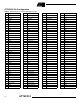
AT75C310 Pin Configuration Table 1.
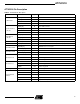
AT75C310 AT75C310 Pin Description Table 2. AT75C310 Pin Description Block Pin Name Type Function A[21:0] O Address Bus D[15:0] I/O Data Bus NREQ I Bus Request NGNT O Bus Grant NRAS[1:0] O Row Address Strobe NCAS[1:0] O Column Address Strobe NDWE O DRAM Write Enable NDOE O DRAM Output Enable NCE[3:0] O Chip Selects NWE[1:0] O Byte Select/Write Enable NSOE O SRAM Output Enable I/O Port A PA[12:0] I/O General Purpose I/O Lines.
Table 2.
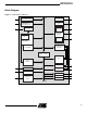
AT75C310 Block Diagram Figure 1.
Architectural Overview The AT75C310 architecture consists of two main buses, the Advanced System Bus (ASB) and the Advanced Peripheral Bus (APB). The ASB is designed for maximum performance. It interfaces the processor with the on-chip DSP subsystems and the external memories and devices by means of the External Bus Interface (EBI). The APB is designed for accesses to on-chip peripherals and is optimized for low power consumption. The AMBA™ Bridge provides an interface between the ASB and the APB.
AT75C310 Memory Map The memory map is divided into memory regions of 64 megabytes. The top seven memory regions are reserved and subdivided for internal memory blocks or peripherals within the AT75C310. The AT75C310 can define up to six other active external memory regions by means of the static memory controller and DRAM memory controller. The memory map assumes default values on reset. External memory regions can be reprogrammed to other base addresses.
Peripheral Memory Map The register maps for each peripheral are described in the corresponding sections of this datasheet. The peripheral memory map has 16KB reserved for each peripheral. Table 4.
AT75C310 Initialization Reset initializes the user interface registers to their default states as defined in the peripheral sections of this datasheet and forces the ARM7TDMI to perform the next instruction fetch from address zero. Except for the program counter, the ARM core registers do not have defined reset states. When reset is active, the inputs of the AT75C310 must be held at valid logic levels. There are three ways in which the AT75C310 can enter reset: 1. Hardware reset.
Clocking The AT75C310 uses an external 16 MHz crystal (XCLK) and two on-chip PLLs to generate the internal clocks. One PLL generates a 96 MHz clock that is divided down to produce the ARM clocks and the other produces an 80 MHz clock used to generate the Oak and Codec interface clocks. The ARM core runs at 24 MHz whereas the DSP subsystems run at 40 MHz. Note that there is a common synchronous mode where the ARM and OAK systems both run from the Oak PLL.
AT75C310 Boot Mode When the reset pin is deasserted, i.e., when the AT75C310 exits from reset state, the NDSRA/BOOTN pin is sampled. If NDSRA/BOOTN is high, the ARM starts fetching from address 0x00000000, which corresponds to the external memory. In a typical application, the external memory located at 0x00000000 is a nonvolatile memory containing the application. If NDSRA/BOOTN is low, the internal boot ROM is remapped to 0x00000000 and the internal boot program is executed.
AT75C310 Mode Controller The mode controller is a memory-mapped peripheral which sits on the APB. It is used to configure the mode in which the AT75C310 operates. Table 5.
AT75C310 • LP: Low Power Mode When high, the ARM is clocked at the low-power frequency. The DMC clock is disabled so the DRAM refresh is also disabled. This field can only be set to high. Writing a zero to this field has no effect. Low-power mode can only be exited by a reset. See the section “Clocking” on page 10 for more details. • LPCS: Low Power Clock Select This field is used to select a slower clock frequency for the ARM system clock.
ID Register Register Name: SIAP_ID 31 30 29 28 27 26 25 24 – – – – – – – – 23 22 21 20 19 18 17 16 – – – – – – – – 15 14 13 12 11 10 9 8 PKG – – – – – – – 7 6 5 4 3 2 1 0 – – – – – VERS VERS VERS • PKG: Package This bit reflects the state of the data bus width signal DBW and indicates the AT75C310 package size, 1 for the 240lead PQFP option and 0 for the 160-lead PQFP option.
AT75C310 EBI: External Bus Interface The EBI generates the signals which control access to the external memory or peripheral devices. The EBI is fully programmable and can address up to 64 megabytes. Its main characteristic is to allow the connection of both static and dynamic memories on the same bus. The address and data lines are shared between static and dynamic devices whereas the control lines are distinct.
Signal Interface Table 6. Signal Interface FPDRAM Description Type A[23:0] Address bus O D[31:0] Data bus I/O D[15:0] used when Data Bus Width is 16 NCE[3:0] Active low chip enables O NCE[3] can be configured for LCD interface mode NWE[3:0] Active low byte select/write strobe signals O NWR Active low write strobe signals O NSOE Active low read enable signal O NWAIT Active low wait signal I Data Bus Width A data bus width of 32 or 16 bits can be selected for each chip select.
AT75C310 Read Protocols The SMC provides two alternative protocols for external memory read access: standard and early read. The difference between the two protocols lies in the timing of the NSOE (read cycle) waveform. The protocol is selected by the DRP field in the memory control register (SMC_MCR) and is valid for all memory devices. Standard read protocol is the default protocol after reset.
External Wait The NWAIT input can be used to add wait states at any time NWAIT is active low and is detected on the rising edge of the clock. If NWAIT is low at the rising edge of the clock, the SMC adds a wait state and does not change the output signals. • Chip Select Change Wait States A chip select wait state is automatically inserted when consecutive accesses are made to two different external memories and no wait states have been inserted. If wait states have been inserted (e.g.
AT75C310 SMC Chip Select Register Register Name: SMC_CSR0..SMC_CSR3 31 30 29 28 27 26 25 24 19 18 17 16 – – – LCD 10 9 BA 23 22 21 20 BA • 15 14 13 12 – – CSEN BAT 7 6 5 4 PAGES – WSE 11 8 TDF 3 NWS 2 PAGES 1 0 DBW DBW: Data Bus Width DBW • • Data Bus Width 0 0 Reserved 0 1 16-bit external bus 1 0 32-bit external bus 1 1 Reserved WSE: Wait State Enable NWS: Number of Wait States This field is valid only if WSE is set.
• PAGES: Page Size PAGES • Page Size Base Address 0 0 1 MB BA[31 - 20] 0 1 4 MB BA[31 - 22] 1 0 16 MB BA[31 - 24] 1 1 Reserved – TDF: Data Float Output Time TDF • Cycles after Transfer 0 0 0 0 0 0 1 1 0 1 0 2 0 1 1 3 1 0 0 4 1 0 1 5 1 1 0 6 1 1 1 7 BAT: Byte Access Mode 0 = Byte-write Mode 1 = Byte-select Mode • CSEN: Chip Select Enable Active high • LCD: LCD Mode Enable Active high. SMC_CSR3 only.
AT75C310 SMC Memory Control Register Register Name: • SMC_MCR 31 30 29 28 27 26 25 24 – – – – – – – – 23 22 21 20 19 18 17 16 – – – – – – – – 15 14 13 12 11 10 9 8 – – – – – – – – 7 6 5 4 3 2 1 0 – – – DRP – – – – DRP: Data Read Protocol 0 = Standard Read Mode 1 = Early Read Mode 21
Switching Waveforms Figure 3 shows a write to memory 0, followed by a write and a read to memory 1. SMC_CSR0 is programmed for one wait state with BAT = 0 and DFT = 0. SMC_CSR1 is programmed for zero wait states with BAT = 1 and DFT = 0. SMC_MCR is programmed for early reads from all memories. The write to memory 0 is a 32-bit word access and, therefore, all four NWE strobes are active. As BAT = 0, they are configured as write strobes and have the same timing as NWR.
AT75C310 Figure 4 shows a write and a read to memory 0, followed by a read and a write to memory 1. SMC_CSR0 is programmed for zero wait states with BAT = 0 and DFT = 0. SMC_CSR1 is programmed for zero wait states with BAT = 1 and DFT = 1. SMC_MCR is programmed for normal reads from all memories The write to memory 0 is a byte access and, therefore, only one NWE strobe is active. As BAT = 0, they are configured as write strobes and have the same timing as NWR.
DMC: Dynamic Memory Controller The ARM can access external DRAM by means of the DRAM memory controller. The DMC sits on the ASB bus and provides a glueless memory interface to external EDO DRAM using the common address and data buses. The AT75C310 supports two DRAM memory regions, each with its own RAS signal. Both DRAM regions share the same CAS, OE, WE, address and data signals.
AT75C310 DRAM Memory Region Configuration Register For each of the two DRAM memory regions there is a memory-mapped register. Register Name: DMC_MR0..
DRAM Common Configuration Register (DMC_CR) The Common Configuration Register defines parameters which are common to the two DRAM regions. Register Name: DMC_CR Reset Value is 0x00000000 31 30 29 28 27 26 25 24 – – – – – – – – 23 22 21 20 19 18 17 16 – – – – – – – – 15 14 13 12 11 10 9 8 – – – – – – – – 7 6 5 4 3 2 1 0 – – – – – ROR BBR DBW • DBW: Data Bus Width When high, the DRAM data bus is 32 bits wide.
AT75C310 Dynamic Memory Accesses Figure 5 and Figure 6 describe the different bus operations that can be performed by DMC. Write Access Followed by Burst Read Access Figure 5 shows a write to DRAM0 followed by a burst of two reads from the same device. The write access takes two clock cycles. During the first cycle, the row address is output and the RAS strobe is asserted. In the next cycle, the column address is output and the CAS strobes are asserted.
Read and Write Accesses Followed by CAS before RAS Refresh Figure 6 shows a read access followed by a write. As the accesses are to different devices, there is no need for a precharge cycle. Figure 6. Read Access Followed by a Write BCLK A RAS0 RAS1 CAS0 CAS1 CAS2 CAS3 NDOE NDWE D (SIAP) D (MEM) 28 AT75C310 The read is a byte access (one CAS strobe is active) and the write is a half-word access (two CAS strobes are active).
AT75C310 AIC: Advanced Interrupt Controller The AT75C310 has an eight-level priority, individually maskable interrupt controller. This feature substantially reduces the software and real-time overhead in handling internal and external interrupts. The interrupt controller is connected to the NFIQ (fast interrupt request) and the NIRQ (standard interrupt request) inputs of the ARM7TDMI processor. The processor’s NFIQ line can only be asserted by the external fast interrupt request input FIQ.
Table 11.
AT75C310 Priority Controller Interrupt Clearing and Setting The NIRQ line is controlled by an eight-level priority encoder. Each source has a programmable priority level of 7 to 0. Level 7 is the highest priority and level 0 the lowest. When the AIC receives more than one unmasked interrupt at a time, the interrupt with the highest priority is serviced first. If both interrupts have equal priority, the interrupt with the lowest interrupt source number is serviced first.
code then checks the interrupt number and branches to the required service routine. 6. The service routine should start by saving the Link Register (R14_irq) and the SPSR (SPSR_irq). Note that the Link Register must be decremented by four when it is saved if it is to be restored directly into the Program Counter at the end of the interrupt. Alternatively, this can be done at the start of the default handler. 7.
AT75C310 AIC User Interface Base Address: 0xFF030000 Table 12.
AIC Source Mode Register Register Name: Access Type: Reset Value: AIC_SMR0..AIC_SMR31 Read/write 0 31 30 29 28 27 26 25 24 – – – – – – – – 23 22 21 20 19 18 17 16 – – – – – – – – 15 14 13 12 11 10 9 8 – – – – – – – – 7 6 5 4 3 2 1 0 – – – • SRCTYPE PRIOR PRIOR: Priority Level Programs the priority level for all sources except source 0 (FIQ). The priority level can be between 0 (lowest) and 7 (highest).
AT75C310 AIC FIQ Vector Register Register Name: Access Type: Reset Value: 31 AIC_FVR Read-only 0 30 29 28 27 26 25 24 19 18 17 16 11 10 9 8 3 2 1 0 FIQV 23 22 21 20 FIQV 15 14 13 12 FIQV 7 6 5 4 FIQV • FIQV: FIQ Vector Register FIQ = 0x00000000 if FIQ active FIQ = 0xFFFFFFFF otherwise AIC Interrupt Status Register Register Name: Access Type: Reset Value: AIC_ISR Read-only 0 31 30 29 28 27 26 25 24 – – – – – – – – 23 22 21 20 19 18 17 16 – – – –
AIC Interrupt Pending Register Register Name: Access Type: Reset Value: • AIC_IPR Read-only Undefined 31 30 29 28 27 26 25 24 – – – – – – – – 23 22 21 20 19 18 17 16 – – – – – – – – 15 14 13 12 11 10 9 8 PIOBIRQ UBIRQ OAKBIRQ OAKAIRQ – IRQ0 SPIIRQ LCDIRQ 7 6 5 4 3 2 1 0 PIOAIRQ TC2IRQ TC1IRQ TC0IRQ UAIRQ SWIRQ WDIRQ FIQ Interrupt Pending 0 = Corresponding interrupt is inactive 1 = Corresponding interrupt is pending AIC Interrupt Mask Regist
AT75C310 AIC Core Interrupt Status Register Register Name: Access Type: Reset Value: • AIC_CISR Read-only 0 31 30 29 28 27 26 25 24 – – – – – – – – 23 22 21 20 19 18 17 16 – – – – – – – – 15 14 13 12 11 10 9 8 – – – – – – – – 7 6 5 4 3 2 1 0 – – – – – – NIRQ NFIQ NFIQ: NFIQ Status 0 = NFIQ line inactive 1 = NFIQ line active • NIRQ: NIRQ Status 0 = NIRQ line inactive 1 = NIRQ line active AIC Interrupt Enable Command Register Register Name:
AIC Interrupt Disable Command Register Register Name: Access Type: • AIC_IDCR Write-only 31 30 29 28 27 26 25 24 – – – – – – – – 23 22 21 20 19 18 17 16 – – – – – – – – 15 14 13 12 11 10 9 8 – – – – – – – – 7 6 5 4 3 2 1 0 – – – – – – NIRQ NFIQ NFIQ: NFIQ Status 0 = NFIQ line inactive 1 = NFIQ line active • NIRQ: NIRQ Status 0 = NIRQ line inactive 1 = NIRQ line active AIC Interrupt Clear Command Register Register Name: Access Type: • AI
AT75C310 AIC Interrupt Set Command Register Register Name: Access Type: • AIC_ISCR Write-only 31 30 29 28 27 26 25 24 – – – – – – – – 23 22 21 20 19 18 17 16 – – – – – – – – 15 14 13 12 11 10 9 8 – – – – – – – – 7 6 5 4 3 2 1 0 – – – – – – NIRQ NFIQ NFIQ: NFIQ Status 0 = NFIQ line inactive 1 = NFIQ line active • NIRQ: NIRQ Status 0 = NIRQ line inactive 1 = NIRQ line active AIC End of Interrupt Command Register Register Name: Access Type:
PIO: Parallel I/O Controller The AT75C310 has 23 programmable I/O lines. Three pins on the AT75C310 are dedicated as general-purpose I/O pins. Other I/O lines are multiplexed with an external signal of a peripheral to optimize the use of available package pins. Refer to Table 13 and Table 14 on page 42. These lines are controlled by two separate and identical PIO controllers, PIO A and PIO B. Each PIO controller also provides an internal interrupt signal to the AIC.
AT75C310 Figure 8.
Table 13.
AT75C310 PIO User Interface PIO Controller A Base Address: 0xFF00C000 PIO Controller B Base Address: 0xFF010000 Table 15.
PIO Enable Register Register Name: Access Type: PIO_PER Write-only 31 30 29 28 27 26 25 24 P31 P30 P29 P28 P27 P26 P25 P24 23 22 21 20 19 18 17 16 P23 P22 P21 P20 P19 P18 P17 P16 15 14 13 12 11 10 9 8 P15 P14 P13 P12 P11 P10 P9 P8 7 6 5 4 3 2 1 0 P7 P6 P5 P4 P3 P2 P1 P0 This register is used to enable individual pins to be controlled by the PIO controller instead of the associated peripheral.
AT75C310 PIO Status Register Register Name: Access Type: PIO_PSR Read-only 31 30 29 28 27 26 25 24 P31 P30 P29 P28 P27 P26 P25 P24 23 22 21 20 19 18 17 16 P23 P22 P21 P20 P19 P18 P17 P16 15 14 13 12 11 10 9 8 P15 P14 P13 P12 P11 P10 P9 P8 7 6 5 4 3 2 1 0 P7 P6 P5 P4 P3 P2 P1 P0 This register indicates which pins are enabled for PIO control. This register is updated when PIO lines are enabled or disabled.
PIO Output Disable Register Register Name: Access Type: PIO_ODR Write-only 31 30 29 28 27 26 25 24 P31 P30 P29 P28 P27 P26 P25 P24 23 22 21 20 19 18 17 16 P23 P22 P21 P20 P19 P18 P17 P16 15 14 13 12 11 10 9 8 P15 P14 P13 P12 P11 P10 P9 P8 7 6 5 4 3 2 1 0 P7 P6 P5 P4 P3 P2 P1 P0 This register is used to disable PIO output drivers. If the pin is driven by the peripheral, this has no effect on the pin, but the information is stored.
AT75C310 PIO Input Filter Enable Register Register Name: Access Type: PIO_IFER Write-only 31 30 29 28 27 26 25 24 P31 P30 P29 P28 P27 P26 P25 P24 23 22 21 20 19 18 17 16 P23 P22 P21 P20 P19 P18 P17 P16 15 14 13 12 11 10 9 8 P15 P14 P13 P12 P11 P10 P9 P8 7 6 5 4 3 2 1 0 P7 P6 P5 P4 P3 P2 P1 P0 This register is used to enable input glitch filters. It affects the pin whether or not the PIO is enabled.
PIO Input Filter Status Register Register Name: Access Type: Reset Value: PIO_IFSR Read-only 0 31 30 29 28 27 26 25 24 P31 P30 P29 P28 P27 P26 P25 P24 23 22 21 20 19 18 17 16 P23 P22 P21 P20 P19 P18 P17 P16 15 14 13 12 11 10 9 8 P15 P14 P13 P12 P11 P10 P9 P8 7 6 5 4 3 2 1 0 P7 P6 P5 P4 P3 P2 P1 P0 This register indicates which pins have glitch filters selected.
AT75C310 PIO Clear Output Data Register Register Name: Access Type: PIO_CODR Write-only 31 30 29 28 27 26 25 24 P31 P30 P29 P28 P27 P26 P25 P24 23 22 21 20 19 18 17 16 P23 P22 P21 P20 P19 P18 P17 P16 15 14 13 12 11 10 9 8 P15 P14 P13 P12 P11 P10 P9 P8 7 6 5 4 3 2 1 0 P7 P6 P5 P4 P3 P2 P1 P0 This register is used to clear PIO output data.
PIO Pin Data Status Register Register Name: Access Type: Reset Value: PIO_PDSR Read-only Undefined 31 30 29 28 27 26 25 24 P31 P30 P29 P28 P27 P26 P25 P24 23 22 21 20 19 18 17 16 P23 P22 P21 P20 P19 P18 P17 P16 15 14 13 12 11 10 9 8 P15 P14 P13 P12 P11 P10 P9 P8 7 6 5 4 3 2 1 0 P7 P6 P5 P4 P3 P2 P1 P0 This register shows the state of the physical pin of the chip.
AT75C310 PIO Interrupt Disable Register Register Name: Access Type: PIO_IDR Write-only 31 30 29 28 27 26 25 24 P31 P30 P29 P28 P27 P26 P25 P24 23 22 21 20 19 18 17 16 P23 P22 P21 P20 P19 P18 P17 P16 15 14 13 12 11 10 9 8 P15 P14 P13 P12 P11 P10 P9 P8 7 6 5 4 3 2 1 0 P7 P6 P5 P4 P3 P2 P1 P0 This register is used to disable PIO interrupts on the corresponding pin. It has an effect whether the PIO is enabled or not.
PIO Interrupt Status Register Register Name: Access Type: Reset Value: PIO_ISR Read-only 0 31 30 29 28 27 26 25 24 P31 P30 P29 P28 P27 P26 P25 P24 23 22 21 20 19 18 17 16 P23 P22 P21 P20 P19 P18 P17 P16 15 14 13 12 11 10 9 8 P15 P14 P13 P12 P11 P10 P9 P8 7 6 5 4 3 2 1 0 P7 P6 P5 P4 P3 P2 P1 P0 This register indicates for each pin when a logic value change has been detected (rising or falling edge).
AT75C310 USART: Universal Synchronous/Asynchronous Receiver/Transmitter The AT75C310 provides two identical, full-duplex, universal synchronous/asynchronous receiver/transmitters as USART A and USART B. These peripherals sit on the APB bus but are also connected to the ASB bus and thus the external memory via the PDC.
Pin Description Each USART channel has the following external signals: Table 16. USART External Signals Signal Name Signal Description SCK USART Serial Clock. Can be configured as input or output.
AT75C310 Table 17. Clock Generator Table CD = 24 x 106/ 16 x Baud Rate Actual CD Actual Baud Rate (bps) Error (bps) % Error 9600 156.25 156 9615.4 15.4 0.16 19200 78.125 78 19230.8 30.8 0.16 38400 39.06 39 38461.5 61.5 0.16 57600 26.04 26 57692.3 92.3 0.16 Required Baud Rate (bps) 115200 13.02 13 115384.6 184.6 0.16 Notes: 1. CD = clock driver 2.
Receiver Asynchronous Receiver The USART is configured for asynchronous operation when SYNC = 0 (bit 7 of US_MR). In asynchronous mode, the USART detects the start of a received character by sampling the RXD signal until it detects a valid start bit. A low level (space) on RXD is interpreted as a valid start bit if it is detected for more than seven cycles of the sampling clock, which is 16 times the baud rate. Hence, a space which is longer than 7/16 of the bit period is detected as a valid start bit.
AT75C310 Time-out This function allows an idle condition on the RXD line to be detected. The maximum delay for which the USART should wait for a new character to arrive while the RXD line is inactive (high level) is programmed in US_RTOR (Receiver Time-out). When this register is set to 0, no time-out is detected. Otherwise, the receiver waits for a first character and then initializes a counter which is decremented at each bit period and reloaded at each byte reception.
Break A break condition is a low signal level which has a duration of at least one character (including start/stop bits and parity). Transmit Break The transmitter generates a break condition on the TXD line when STTBRK is set in US_CR (Control Register). In this case, the character present in the Transmit Shift Register is completed before the line is held low. To cancel a break condition on the TXD line, the STPBRK command in US_CR must be set.
AT75C310 Interrupt Generation Each status bit in US_CSR has a corresponding bit in US_IER (Interrupt Enable) and US_IDR (Interrupt Disable) which controls the generation of interrupts by asserting the USART interrupt line connected to the AIC. US_IMR (Interrupt Mask Register) indicates the status of the corresponding bits. When a bit is set in US_CSR and the same bit is set in US_IMR, the interrupt line is asserted. Figure 15.
Modem Control and Status Signals NCTS: Clear to Send When low, this indicates that the modem or data set is ready to exchange data. The NCTS signal is a modem status input, conditions of which can be tested by the CPU reading bit 4 (CTS) of the Modem Status Register. Bit 4 is the complement of the NCTS signal. Bit 0 (DCTS) of the Modem Status Register indicates whether the NCTS input has changed state since the previous reading of the Modem Status Register. NCTS has no effect on the transmitter.
AT75C310 USART User Interface Base Address USART A: Base Address USART B: Offset Notes: 0xFF018000 0xFF01C000 Register Description Register Name Access Reset State 0x00 Control Register US_CR Write-only – 0x04 Mode Register US_MR Read/write 0 0x08 Interrupt Enable Register US_IER Write-only – 0x0C Interrupt Disable Register US_IDR Write-only – 0x10 Interrupt Mask Register US_IMR Read-only 0 0x14 Channel Status Register US_CSR Read-only 0x18(1) 0x18 Receiver Holding Regi
USART Control Register Name: Access Type: • • • • • • • • • • • 62 US_CR Write-only 31 30 29 28 27 26 25 24 – – – – – – – – 23 22 21 20 19 18 17 16 – – – – – – – – 15 14 13 12 11 10 9 8 – – – SENDA STTTO STPBRK STTBRK RSTSTA 7 6 5 4 3 2 1 0 TXDIS TXEN RXDIS RXEN RSTTX RSTRX – – RSTRX: Reset Receiver 0 = No effect. 1 = The receiver logic is reset. RSTTX: Reset Transmitter 0 = No effect. 1 = The transmitter logic is reset.
AT75C310 USART Mode Register Name: Access Type: US_MR Read/write 31 30 29 28 27 26 25 24 – – – – – – – – 23 22 21 20 19 18 17 16 – – – – – CLKO MODE9 – 14 13 12 11 10 9 15 CHMODE NBSTOP 7 6 5 CHRL • 4 USCLKS 8 SYNC 3 2 1 0 – – – – USCLKS: Clock Selection (Baud Rate Generator Input Clock) USCLKS • PAR Selected Clock 0 0 ACLK 0 1 ACLK/8 1 X External (SCK) CHRL: Character Length CHRL Character Length 0 0 Five bits 0 1 Six bits 1 0
• NBSTOP: Number of Stop Bits The interpretation of the number of stop bits depends on SYNC. NBSTOP Asynchronous (SYNC = 0) Synchronous (SYNC = 1) 0 0 1 stop bit 1 stop bit 0 1 1.5 stop bits Reserved 1 0 2 stop bits 2 stop bits 1 1 Reserved Reserved • CHMODE: Channel Mode CHMODE • Mode Description 0 0 Normal Mode The USART Channel operates as an Rx/Tx USART. 0 1 Automatic Echo Receiver Data Input is connected to TXD pin.
AT75C310 USART Interrupt Enable Register Name: Access Type: • US_IER Write-only 31 30 29 28 27 26 25 24 – – – – – – – – 23 22 21 20 19 18 17 16 – – – – – – – – 15 14 13 12 11 10 9 8 – – – – – DMSI TXEMPTY TIMEOUT 7 6 5 4 3 2 1 0 PARE FRAME OVRE ENDTX ENDRX RXBRK TXRDY RXRDY RXRDY: Enable RXRDY Interrupt 0 = No effect. 1 = Enables RXRDY Interrupt. • TXRDY: Enable TXRDY Interrupt 0 = No effect.
USART Interrupt Disable Register Name: Access Type: • US_IDR Write-only 31 30 29 28 27 26 25 24 – – – – – – – – 23 22 21 20 19 18 17 16 – – – – – – – – 15 14 13 12 11 10 9 8 – – – – – DMSI TXEMPTY TIMEOUT 7 6 5 4 3 2 1 0 PARE FRAME OVRE ENDTX ENDRX RXBRK TXRDY RXRDY RXRDY: Disable RXRDY Interrupt 0 = No effect. 1 = Disables RXRDY Interrupt. • TXRDY: Disable TXRDY Interrupt 0 = No effect.
AT75C310 USART Interrupt Mask Register Name: Access Type: • US_IMR Read-only 31 30 29 28 27 26 25 24 – – – – – – – – 23 22 21 20 19 18 17 16 – – – – – – – – 15 14 13 12 11 10 9 8 – – – – – DMSI TXEMPTY TIMEOUT 7 6 5 4 3 2 1 0 PARE FRAME OVRE ENDTX ENDRX RXBRK TXRDY RXRDY RXRDY: RXRDY Interrupt Mask 0 = RXRDY Interrupt is disabled. 1 = RXRDY Interrupt is enabled. • TXRDY: TXRDY Interrupt Mask 0 = TXRDY Interrupt is disabled.
USART Channel Status Register Name: Access Type: • US_CSR Read-only 31 30 29 28 27 26 25 24 – – – – – – – – 23 22 21 20 19 18 17 16 – – – – – – – – 15 14 13 12 11 10 9 8 – – – – – DMSI TXEMPTY TIMEOUT 7 6 5 4 3 2 1 0 PARE FRAME OVRE ENDTX ENDRX RXBRK TXRDY RXRDY RXRDY: Receiver Ready 0 = No complete character has been received since the last read of the US_RHR or the receiver is disabled.
AT75C310 • TXEMPTY: Transmitter Empty 0 = There are characters in either US_THR or the Transmit Shift Register or a break is being transmitted. 1 = There are no characters in US_THR and the Transmit Shift Register and break is not active. Equal to zero when the USART is disabled or at reset. Transmitter Enable command (in US_CR) sets this bit to one. • DMSI: Delta Modem Status Indication Interrupt 0 = No effect.
USART Receiver Holding Register Name: Access Type: US_RHR Read-only 31 30 29 28 27 26 25 24 – – – – – – – – 23 22 21 20 19 18 17 16 – – – – – – – – 15 14 13 12 11 10 9 8 – – – – – – – RXCHR 7 6 5 4 3 2 1 0 RXCHR • RXCHR: Received Character Last character received if RXRDY is set. When number of data bits is less than eight, the bits are right-aligned. All unused bits read as zero.
AT75C310 USART Baud Rate Generator Register Name: Access Type: US_BRGR Read/write 31 30 29 28 27 26 25 24 – – – – – – – – 23 22 21 20 19 18 17 16 – – – – – – – – 15 14 13 12 11 10 9 8 3 2 1 0 CD 7 6 5 4 CD • CD: Clock Divisor This register has no effect if synchronous mode is selected with an external clock.
USART Receiver Time-out Register Name: Access Type: US_RTOR Read/write 31 30 29 28 27 26 25 24 – – – – – – – – 23 22 21 20 19 18 17 16 – – – – – – – – 15 14 13 12 11 10 9 8 – – – – – – – – 7 6 5 4 3 2 1 0 TO • TO: Time-out Value When a value is written to this register, a Start Time-out command is automatically performed. TO 0 1 - 255 Effect Disables the RX Time-out function.
AT75C310 USART Transmitter Time-guard Register Name: Access Type: US_TTGR Read/write 31 30 29 28 27 26 25 24 – – – – – – – – 23 22 21 20 19 18 17 16 – – – – – – – – 15 14 13 12 11 10 9 8 – – – – – – – – 7 6 5 4 3 2 1 0 27 26 25 24 19 18 17 16 11 10 9 8 3 2 1 0 TG • TG: Time-guard Value TG 0 1 - 255 Disables the TX Time-guard function. TXD is inactive high after the transmission of each character for the time-guard duration.
USART Receive Counter Register Name: Access Type: US_RCR Read/write 31 30 29 28 27 26 25 24 – – – – – – – – 23 22 21 20 19 18 17 16 – – – – – – – – 15 14 13 12 11 10 9 8 3 2 1 0 27 26 25 24 19 18 17 16 11 10 9 8 3 2 1 0 RXCTR 7 6 5 4 RXCTR • RXCTR: Receive Counter RXCTR must be loaded with the size of the receive buffer. 0: Stop peripheral data transfer dedicated to the receiver. 1 - 65535: Start peripheral data transfer if RXRDY is active.
AT75C310 USART Transmit Counter Register Name: Access Type: US_TCR Read/write 31 30 29 28 27 26 25 24 – – – – – – – – 23 22 21 20 19 18 17 16 – – – – – – – – 15 14 13 12 11 10 9 8 3 2 1 0 TXCTR 7 6 5 4 TXCTR • TXCTR: Transmit Counter TXCTR must be loaded with the size of the transmit buffer. 0: Stop peripheral data transfer dedicated to the transmitter. 1 - 65535: Start peripheral data transfer if TXRDY is active.
Modem Control Register Register Name: US_MC 31 30 29 28 27 26 25 24 – – – – – – – – 23 22 21 20 19 18 17 16 – – – – – – – – 15 14 13 12 11 10 9 8 – – – – – – – – 7 6 5 4 3 2 1 0 – – FCM – – – RTS DTR This register controls the interface with the modem or data set (or a peripheral device emulating a modem). The contents of the Control Register are indicated below. • DTR: Data Terminal Ready This bit controls the NDTR output.
AT75C310 Modem Status Register Register Name: US_MS 31 30 29 28 27 26 25 24 – – – – – – – – 23 22 21 20 19 18 17 16 – – – – – – – – 15 14 13 12 11 10 9 8 – – – – – – – FCMS 7 6 5 4 3 2 1 0 DCD RI DSR CTS DDCD TERI DDSR DCTS This register provides the current state of the control lines from the modem (or peripheral device) to the CPU.
TC: Timer/Counter The AT75C310 features a timer/counter block which includes three identical 16-bit timer/counter channels. Each channel can be independently programmed to perform a wide range of functions including frequency measurement, event counting, interval measurement, pulse generation, delay timing and pulse-width modulation. Each timer/counter channel has three external clock inputs, five internal clock inputs, and two multi-purpose input/output signals that can be configured by the user.
AT75C310 Signal Name Description Channel Signal Description XC0, XC1, XC2 External Clock Inputs TIOA Capture Mode: General-purpose input Waveform Mode: General-purpose output TIOB Capture Mode: General-purpose input Waveform Mode: General-purpose input/output INT SYNC Interrupt signal output Synchronization input signal Block Signal TCLK0, TCLK1, TCLK2 Note: External Clock Inputs TIOA0 TIOA signal for Channel 0 TIOB0 TIOB signal for Channel 0 TIOA1 TIOA signal for Channel 1 TIOB1 TIOB si
Figure 17. Clock Selection Figure 18. Clock Control Selected Clock CLKS Trigger CLKI ACLK/2 ACLK/8 CLKSTA ACLK/32 ACLK/128 CLKEN CLKDIS Selected Clock ACLK/1024 XC0 Q XC1 XC2 Q S S R R BURST 1 Counter Clock Clock Control The clock of each counter can be controlled in two different ways: it can be enabled/disabled and started/stopped. 1. The clock can be enabled or disabled by the user with the CLKEN and the CLKDIS commands in the Control Register.
AT75C310 Capture Mode Capture mode is entered by clearing the WAVE parameter in TC_CMR (Channel Mode Register). Capture mode allows the TC channel to perform measurements such as pulse timing, frequency, period, duty cycle and phase on TIOA and TIOB signals which are inputs. Figure 19 shows the configuration of the TC Channel when programmed in capture mode. Capture Registers A and B (RA and RB) Registers A and B are used as capture registers.
Figure 19.
AT75C310 Waveform Mode Waveform mode is entered by setting the WAVE parameter in TC_CMR (Channel Mode Register). Waveform mode allows the TC channel to generate one or two PWM signals with the same frequency and independently programmable duty cycles or different types of oneshot or repetitive pulses. In this mode, TIOA is configured as output and TIOB is defined as output if it is not used as an external event (EEVT parameter in TC_CMR).
CLKSTA ACLK/2 CLKEN CLKDIS ACPC CLKI ACLK/8 Q S CPCDIS Q XC0 R S ACPA R XC1 XC2 CPCSTOP AEEVT MTIOA TIOA BURST Register A Register B Register C Compare RA = Compare RB = Compare RC = ASWTRG 1 16-bit Counter CLK RESET SWTRG OVF BCPC SYNC Trig MTIOB BCPB CPCTRG EEVT BEEVT CPBS CPCS CPAS COVFS BSWTRG TC_IMR TIOB TC_SR Edge Detector ENETRG ETRGS EEVTEDG Timer/Counter Channel INT Output Controller AT75C310 ACLK/128 ACLK/1024 Output Controller ACLK/32 TIOB Figure
AT75C310 TC User Interface TC Base Address: 0xFF014000 Table 18. TC Global Memory Map Offset Channel/Register Name Access Reset State 0x00 TC Channel 0 See Table 19 0x40 TC Channel 1 See Table 19 0x80 TC Channel 2 See Table 19 0xC0 TC Block Control Register TC_BCR Write-only – 0xC4 TC Block Mode Register TC_BMR Read/write 0 TC_BCR (Block Control Register) and TC_BMR (Block Mode Register) control the TC block. TC channels are controlled by the registers listed in Table 19.
TC Block Control Register Register Name: Access Type: • TC_BCR Write-only 31 30 29 28 27 26 25 24 – – – – – – – – 23 22 21 20 19 18 17 16 – – – – – – – – 15 14 13 12 11 10 9 8 – – – – – – – – 7 6 5 4 3 2 1 0 – – – – – – – SYNC SYNC: Synchro Command 0 = No effect. 1 = Asserts the SYNC signal which generates a software trigger simultaneously for each of the channels.
AT75C310 TC Block Mode Register Register Name: Access Type: • 31 30 29 28 27 26 25 24 – – – – – – – – 23 22 21 20 19 18 17 16 – – – – – – – – 15 14 13 12 11 10 9 8 – – – – – – – – 7 6 5 4 3 2 1 – – TC1XC1S 0 TC0XC0S Signal Connected to XC0 0 0 TCLK0 0 1 None 1 0 TIOA1 1 1 TIOA2 TC1XC1S: External Clock Signal 1 Selection TC1XC1S • TC2XC2S TC0XC0S: External Clock Signal 0 Selection TC0XC0S • TC_BMR Read/write Signal Connected to X
TC Channel Control Register Register Name: Access Type: • TC_CCR Write-only 31 30 29 28 27 26 25 24 – – – – – – – – 23 22 21 20 19 18 17 16 – – – – – – – – 15 14 13 12 11 10 9 8 – – – – – – – – 7 6 5 4 3 2 1 0 – – – – – SWTRG CLKDIS CLKEN CLKEN: Counter Clock Enable Command 0 = No effect. 1 = Enables the clock if CLKDIS is not 1. • CLKDIS: Counter Clock Disable Command 0 = No effect. 1 = Disables the clock.
AT75C310 TC Channel Mode Register: Capture Mode Register Name: Access Type: • TC_CMR Read/write 31 30 29 28 27 26 25 24 – – – – – – – – 23 22 21 20 19 18 17 – – – – 15 14 13 12 11 10 WAVE=0 CPCTRG – – – ABETRG 7 6 5 3 2 LDBDIS LDBSTOP CLKI LDRA 9 8 ETRGEDG 1 0 TCCLKS TCCLKS: Clock Selection TCCLKS • 4 BURST 16 LDRB Clock Selected 0 0 0 ACLK/2 0 0 1 ACLK/8 0 1 0 ACLK/32 0 1 1 ACLK/128 1 0 0 ACLK/1024 1 0 1 XC0 1 1 0 XC1
• ETRGEDG: External Trigger Edge Selection ETRGEDG Edge 0 0 None 0 1 Rising edge 1 0 Falling edge 1 1 Each edge • ABETRG: TIOA or TIOB External Trigger Selection 0 = TIOB is used as an external trigger. 1 = TIOA is used as an external trigger. • CPCTRG: RC Compare Trigger Enable 0 = RC Compare has no effect on the counter and its clock. 1 = RC Compare resets the counter and starts the counter clock. • WAVE = 0 0 = Capture Mode is enabled.
AT75C310 TC Channel Mode Register: Waveform Mode Register Name: Access Type: TC_CMR Read/write 31 30 29 BSWTRG 23 22 20 26 19 AEEVT 25 24 BCPB 18 17 16 ACPC 15 14 13 12 WAVE=1 CPCTRG – ENETRG 7 6 5 CPCDIS CPCSTOP 4 BURST 11 ACPA 10 9 EEVT 3 CLKI 8 EEVTEDG 2 1 0 TCCLKS TCCLKS: Clock Selection TCCLKS • 27 BCPC 21 ASWTRG • 28 BEEVT Clock Selected 0 0 0 ACLK/2 0 0 1 ACLK/8 0 1 0 ACLK/32 0 1 1 ACLK/128 1 0 0 ACLK/1024 1 0 1 XC0 1 1 0 XC1
• • EEVTEDG: External Event Edge Selection EEVTEDG Edge 0 0 None 0 1 Rising edge 1 0 Falling edge 1 1 Each edge EEVT: External Event Selection EEVT TIOB Direction 0 0 TIOB Input(1) 0 1 XC0 Output 1 0 XC1 Output 1 1 XC2 Output Note: • Signal Selected as External Event 1. If TIOB is chosen as the external event signal, it is configured as an input and no longer generates waveforms.
AT75C310 • AEEVT: External Event Effect on TIOA AEEVT • • Effect 0 0 None 0 1 Set 1 0 Clear 1 1 Toggle ASWTRG: Software Trigger Effect on TIOA ASWTRG Effect 0 0 None 0 1 Set 1 0 Clear 1 1 Toggle BCPB: RB Compare Effect on TIOB BCPB • Effect 0 0 None 0 1 Set 1 0 Clear 1 1 Toggle BCPC: RC Compare Effect on TIOB BCPC • Effect 0 0 None 0 1 Set 1 0 Clear 1 1 Toggle BEEVT: External Event Effect on TIOB BEEVT Effect 0 0 None 0 1 Set 1 0 Clear
• 94 BSWTRG: Software Trigger Effect on TIOB BSWTRG Effect 0 0 None 0 1 Set 1 0 Clear 1 1 Toggle AT75C310
AT75C310 TC Counter Value Register Register Name: Access Type: TC_CVR Read-only 31 30 29 28 27 26 25 24 – – – – – – – – 23 22 21 20 19 18 17 16 – – – – – – – – 15 14 13 12 11 10 9 8 3 2 1 0 CV 7 6 5 4 CV • CV: Counter Value CV contains the counter value in real-time.
TC Register B Register Name: Access Type: TC_RB Read-only if WAVE = 0, Read/write if WAVE = 1 31 30 29 28 27 26 25 24 – – – – – – – – 23 22 21 20 19 18 17 16 – – – – – – – – 15 14 13 12 11 10 9 8 3 2 1 0 RB 7 6 5 4 RB • RB: Register B RB contains the Register B value in real-time.
AT75C310 TC Status Register Register Name: Access Type: TC_SR Read/write 31 30 29 28 27 26 25 24 – – – – – – – – 23 22 21 20 19 18 17 16 – – – – – MTIOB MTIOA CLKSTA 15 14 13 12 11 10 9 8 – – – – – – – – 7 6 5 4 3 2 1 0 ETRGS LDRBS LDRAS CPCS CPBS CPAS LOVRS COVFS • COVFS: Counter Overflow Status 0 = No counter overflow has occurred since the last read of the Status Register.
TC Interrupt Enable Register Register Name: Access Type: • TC_IER Write-only 31 30 29 28 27 26 25 24 – – – – – – – – 23 22 21 20 19 18 17 16 – – – – – – – – 15 14 13 12 11 10 9 8 – – – – – – – – 7 6 5 4 3 2 1 0 ETRGS LDRBS LDRAS CPCS CPBS CPAS LOVRS COVFS COVFS: Counter Overflow 0 = No effect. 1 = Enables the Counter Overflow Interrupt. • LOVRS: Load Overrun 0 = No effect. 1 = Enables the Load Overrun Interrupt.
AT75C310 TC Interrupt Disable Register Register Name: Access Type: • TC_IDR Write-only 31 30 29 28 27 26 25 24 – – – – – – – – 23 22 21 20 19 18 17 16 – – – – – – – – 15 14 13 12 11 10 9 8 – – – – – – – – 7 6 5 4 3 2 1 0 ETRGS LDRBS LDRAS CPCS CPBS CPAS LOVRS COVFS COVFS: Counter Overflow 0 = No effect. 1 = Disables the Counter Overflow Interrupt. • LOVRS: Load Overrun 0 = No effect. 1 = Disables the Load Overrun Interrupt (if WAVE = 0).
TC Interrupt Mask Register Register Name: Access Type: • TC_IMR Read-only 31 30 29 28 27 26 25 24 – – – – – – – – 23 22 21 20 19 18 17 16 – – – – – – – – 15 14 13 12 11 10 9 8 – – – – – – – – 7 6 5 4 3 2 1 0 ETRGS LDRBS LDRAS CPCS CPBS CPAS LOVRS COVFS COVFS: Counter Overflow 0 = The Counter Overflow Interrupt is disabled. 1 = The Counter Overflow Interrupt is enabled. • LOVRS: Load Overrun 0 = The Load Overrun Interrupt is disabled.
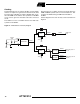
AT75C310 SPI: Serial Peripheral Interface The serial peripheral interface provides communication with external devices in master or slave mode. It also allows communication with external processors or serial Flash. Figure 21. SPI Block Diagram ACLK Serial Peripheral Interface MISO MISO MOSI MOSI SPCK SPCK ACLK/32 APB INT NPCSS NPCSS NPCS1 NPCS1 NPCS2 NPCS2 NPCS3 NPCS3 Advanced Interrupt Controller Table 20.
Master Mode In master mode, the SPI controls data transfers to and from the slave(s) connected to the SPI bus. The SPI drives the chip select(s) to the slave(s) and the serial clock (SPCK). After enabling the SPI, a data transfer begins when the ARM core writes to the SP_TDR (Transmit Data Register). See Table 21. Transmit and receive buffers maintain the data flow at a constant rate with a reduced requirement for high-priority interrupt servicing.
AT75C310 Figure 22.
Figure 23.
AT75C310 Slave Mode In slave mode, the SPI waits for NPCSS to go active low before receiving the serial clock from an external master. In s la ve mode, CPO L, N CPHA and BITS fiel ds of SP_CSR0 are used to define the transfer characteristics. The other chip select registers are not used in slave mode. Figure 24.
Data Transfer Figure 25, Figure 26 and Figure 27 show examples of data transfers. Figure 25. SPI Transfer Format (NCPHA Equals One, Eight Bits per Transfer) 1 SPCK cycle (for reference) 2 3 5 4 6 8 7 SPCK (CPOL=0) SPCK (CPOL=1) MOSI (from master) MSB MISO (from slave) MSB 6 5 4 3 2 1 LSB 6 5 4 3 2 1 LSB X NPCSS (to slave) Figure 26.
AT75C310 Figure 27. Programmable Delays (DLYBCS, DLYBS and DLYBCT) Chip Select 1 Change peripheral Chip Select 2 No change of peripheral SPCK Output DLYBCS DLYBS DLYBCT DLYBCT Clock Generation In master mode, the SPI master clock is either ACLK or ACLK/32 as defined by the MCK32 field of SP_MR. The SPI baud rate clock is generated by dividing the SPI master clock by a value between 4 and 510. The divisor is defined in the SCBR field in each chip select register.
Table 21.
AT75C310 SPI Mode Register Register Name: Access Type: 31 SP_MR Read/write 30 29 28 27 26 19 18 25 24 17 16 DLYBCS • 23 22 21 20 – – – – 15 14 13 12 11 10 9 8 – – – – – – – – 7 6 5 4 3 2 1 0 LLB – – – MCK32 PCSDEC PS MSTR PCS MSTR: Master/Slave Mode 0 = SPI is in slave mode. 1 = SPI is in master mode. MSTR configures the SPI interface for either master or slave mode operation. • PS: Peripheral Select 0 = Fixed Peripheral Select.
• PCS: Peripheral Chip Select This field is only used if Fixed Peripheral Select is active (PS=0). If PCSDEC=0: PCS = xxx0 NPCS[3:0] = 1110 PCS = xx01 NPCS[3:0] = 1101 PCS = x011 NPCS[3:0] = 1011 PCS = 0111 NPCS[3:0] = 0111 PCS = 1111 forbidden (no peripheral is selected) (x = don’t care) If PCSDEC=1: NPCS[3:0] output signals = PCS • DLYBCS: Delay Between Chip Selects This field defines the delay from NPCS inactive to the activation of another NPCS.
AT75C310 SPI Transmit Data Register Register Name: Access Type: SP_TDR Write-only 31 30 29 28 27 26 25 24 – – – – – – – – 23 22 21 20 19 18 17 16 – – – – 15 14 13 12 PCS 11 10 9 8 3 2 1 0 TD 7 6 5 4 TD • TD: Transmit Data Data that is to be transmitted by the SPI interface is stored in this register. Information to be transmitted must be written to the transmit data register in a right-justified format.
SPI Status Register Register Name: Access Type: • SP_SR Read-only 31 30 29 28 27 26 25 24 – – – – – – – – 23 22 21 20 19 18 17 16 – – – – – – – SPIENS 15 14 13 12 11 10 9 8 – – – – – – – – 7 6 5 4 3 2 1 0 – – – – OVRES MODF TDRE RDRF RDRF: Receive Data Register Full 0 = No data has been received since the last read of SP_RDR.
AT75C310 SPI Interrupt Enable Register Register Name: Access Type: • SP_IER Write-only 31 30 29 28 27 26 25 24 – – – – – – – – 23 22 21 20 19 18 17 16 – – – – – – – – 15 14 13 12 11 10 9 8 – – – – – – – – 7 6 5 4 3 2 1 0 – – – – OVRES MODF TDRE RDRF RDRF: Receive Data Register Full Interrupt Enable 0 = No effect. 1 = Enables the Receiver Data Register Full Interrupt. • TDRE: SPI Transmit Data Register Empty Interrupt Enable 0 = No effect.
• MODF: Mode Fault Interrupt Disable 0 = No effect. • OVRES: Overrun Error Interrupt Disable 0 = No effect. 1 = Disables the Mode Fault Interrupt. 1 = Disables the Overrun Error Interrupt.
AT75C310 SPI Chip Select Register Register Name: Access Type: 31 SP_CSR0..SP_CSR1 Read/write 30 29 28 27 26 25 24 19 18 17 16 11 10 9 8 3 2 1 0 – – NCPHA CPOL DLYBCT 23 22 21 20 DLYBS 15 14 13 12 SCBR 7 6 5 4 BITS • CPOL: Clock Polarity 0 = The inactive state value of SPCK is logic level zero. 1 = The inactive state value of SPCK is logic level one. CPOL is used to determine the inactive state value of the serial clock (SPCK).
• BITS[3:0] Bits per Transfer 1101 Reserved 1110 Reserved 1111 Reserved SCBR: Serial Clock Baud Rate In master mode, the SPI interface uses a modulus counter to derive the SPCK baud rate from the SPI master clock (selected between ACLK and ACLK/32). The baud rate is selected by writing a value from 2 to 255 in the field SCBR.
AT75C310 WD: Watchdog Timer The AT75C310 has an internal watchdog timer which can be used to prevent system lock-up if the software becomes trapped in a deadlock. In normal operation, the user reloads the watchdog at regular intervals before the timer overflow occurs.
WD Overflow Mode Register Name: Access: Reset Value: WD_OMR Read/write 0 31 30 29 28 27 26 25 24 – – – – – – – – 23 22 21 20 19 18 17 16 – – – – – – – – 15 14 13 12 11 10 9 8 OKEY 7 6 5 4 OKEY • 3 2 1 0 EXTEN IRQEN RSTEN WDEN WDEN: Watchdog Enable 0 = Watchdog is disabled and does not generate any signals. 1 = Watchdog is enabled and generates enabled signals. • RSTEN: Reset Enable 0 = Generation of an internal reset by the watchdog is disabled.
AT75C310 WD Clock Mode Register Name: Access: Reset Value: WD_CMR Read/write 0 31 30 29 28 27 26 25 24 – – – – – – – – 23 22 21 20 19 18 17 16 – – – – – – – – 15 14 13 12 11 10 9 8 3 2 1 CKEY • 7 6 CKEY – 5 4 HPCV 0 WDCLKS WDCLKS: Clock Selection WDCLKS Clock Selected 0 0 ACLK/8 0 1 ACLK/32 1 0 ACLK/128 1 1 ACLK/1024 • HPCV: High Preload Counter Value Counter is preloaded when watchdog counter is restarted with bits 0 to 11 set (FFF) and b
WD Status Register Name: Access: • WD_SR Read-only 31 30 29 28 27 26 25 24 – – – – – – – – 23 22 21 20 19 18 17 16 – – – – – – – – 15 14 13 12 11 10 9 8 – – – – – – – – 7 6 5 4 3 2 1 0 – – – – – – – WDOVF WDOVF: Watchdog Overflow 0 = No watchdog overflow. 1 = A watchdog overflow has occurred since the last restart of the watchdog counter or since internal or external reset.
AT75C310 WD Enabling Sequence To enable the watchdog timer the sequence is as follows: 1. Disable the watchdog by clearing the bit WDEN: Write 0x2340 to WD_OMR This step is unnecessary if the WD is already disabled (reset state). 2. Initialize the WD Clock Mode Register: Write 0x373C to WD_CMR (HPCV = 15 and WDCLKS = MCK/8) 3. Restart the timer: Write 0xC071 to WD_CR 4.
Dual-port Mailbox Communication between the asynchronous ARM7TDMI and OakDSPCore are via the dual-port mailbox (DPMB). It is assumed that each processor is running asynchronously and that the coherency of communication is maintained by robust software. The DPMB consists of 512 bytes of DPRAM and some memory-mapped registers that configure the DPMB and act as semaphores. The DPMB sits on the ARM7TDMI ASB bus and can be accessed by memory-mapped operations.
AT75C310 Semaphore Operation The DPMB supports semaphore registers to facilitate asynchronous communication between two processors. Each of the eight mailboxes has its own memory-mapped semaphore register. This avoids any need for complex readmodify-write operations. Each semaphore is configured to control message-passing in a single direction, i.e., from the ARM to the Oak when the DPMB ARM-to-Oak flag is set high. When this flag is low, then the direction of transfer is Oak to ARM.
DPMB Register Map Table 23.
AT75C310 DPMB Semaphore Registers The semaphore registers look the same from the ARM and the Oak sides. 31 30 29 28 27 26 25 24 – – – – – – – – 23 22 21 20 19 18 17 16 – – – – – – – – 15 14 13 12 11 10 9 8 – – – – – – – – 7 6 5 4 3 2 1 0 – – – – – OIS AIS Sem • Sem: Semaphore When low, the sender has read and write permission to the mailbox. The recipient has no permission to read or write the associated mailbox.
Assembly Source Code – Boot Program ;----------------------------------------------------------------------------;Cadence Design Systems Ltd. Copyright 1999. All Rights Reserved. ;----------------------------------------------------------------------------;MODULE: bootcode.s ;CREATION DATE: 26 Feb 1999 ;AUTHOR: Kevin Robertson ;DESCRIPTION: This file contains the code to go into the SIAP bootrom - it is used by all the bootrom tests which use a GET to include this file.
AT75C310 B fiqvec ; FIQ ;----------------------------------------------------------------------------; Entry point.
bl rx-poll-timed cmp r2, #Ox16 bne remap ; ; A synch has been received look for the rest of the activation sequence ; bl rx_poll_timed cmp r2, #Ox42 bne remap bl rx_poll_timed cmp, r2, #Ox6f bne remap, bl rx_poll_timed cmp r2, #Ox6f bne remap, bl rx_poll_timed cmp r2, #Ox74 bne remap bl rx_poll_timed cmp r2, #Oxl6 bne remap ;Activation sequence received send the response mov r2, #Ox16 bl sendbyte mov r2, #Ox52 bl send_byte mov r2, #Ox4f bl send_byte mov r2, #Ox4d bl send_byte mov r2, #Oxl6 bl send_byte ; Re
AT75C310 eor r5, r5, r2 mov r2, r2, LSL #8 orr r4, r4, r2 bl rx_poll eor r5, r5, r2 mov r2, r2, LSL #16 orr r4, r4, r2 bl rx_poll eor r5, r5, r2 mov r2, r2, LSL #24 orr r4, r4, r2 ; Store the 32 bit value str r4, [r6l, #4 ; decrement the counter subs r3, r3, #4 b read_loop ;----------------------------------------------------------------------------; End of the Down Load Loop. Now wait for DSR to reset then send the checksum ; for the values which have just been downloaded.
tst rl, #OxO1 beq rx_poll_timed ldr rl, USARTO_RHR_Reg ldr r2, [r1] mov pc, lr ;----------------------------------------------------------------------------; rx_poll ; Wait for a character to be received.
AT75C310 DCD OxFF01800C USARTO_CSR_Reg DCD OxFF018014 USARTO_RHR_Reg DCD OxFF018018 USARTO_THR_Reg DCD OxFF01801C USARTO_BR_Reg DCD OxFF018020 USARTO_ModC_Reg DCD OxFF018040 USARTO_ModS_Reg DCD OxFF018044 SIAP_Mode_Reg DCD OxFFOOOOOO END 131
Atmel Headquarters Atmel Operations Corporate Headquarters Atmel Colorado Springs 2325 Orchard Parkway San Jose, CA 95131 TEL (408) 441-0311 FAX (408) 487-2600 Europe Atmel SarL Route des Arsenaux 41 Casa Postale 80 CH-1705 Fribourg Switzerland TEL (41) 26-426-5555 FAX (41) 26-426-5500 Asia Atmel Asia, Ltd. Room 1219 Chinachem Golden Plaza 77 Mody Road Tsimhatsui East Kowloon Hong Kong TEL (852) 2721-9778 FAX (852) 2722-1369 Japan 1150 E. Cheyenne Mtn. Blvd.