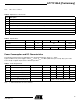
Features • • • • • • • • • • • • • • • Thermal Sensitive Layer Over a 0.35 µm CMOS Array Image Zone: 0.4 x 11.6 mm Image Array: 8 × 232 = 1856 Pixels Pixel Pitch: 50 × 50 µm = 500 dpi Resolution On-chip 8-bit Analog to Digital Converter Serial Peripheral Interface (SPI) - 2 Modes: – Fast Mode at 16 Mbps Max for Imaging – Slow Mode at 200 kbps Max for Navigation and Control Die Size: 1.5 × 15 mm Operating Voltage: 2.3 to 3.6V I/O Voltage: 1.65 to 3.
Table 1.
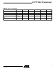
AT77C105A [Preliminary] Figure 1. Typical Application VDDD VDDD 10 kΩ VDD_IO 10 kΩ TESTA IRQ NC VDDD VDD_IO MISO VDDD MOSI 10µF SCK GNDD SSS VDDA FSS VDDA 10µF SCANEN GNDA FPL GND GND RST The pull-up must be implemented for the master controller. The noise should be lower than 30 mV peak to peak on VDDA. Figure 2.
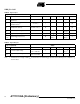
Specifications Table 2. Absolute Maximum Ratings Parameter Power supply voltage Symbol Comments Value VDDD, VDDA -0.5 to 4.6V Front plane FPL GND to VDD +0.5V Digital input SSS, FSS, SCK, MOSI GND to VDD +0.5V VDD_IO GND to VDD +0.5V Tstg -50 to +95°C Input/output pads power supply Storage temperature Lead temperature (soldering 10 seconds) Tleads Do not solder Forbidden Note: Stresses beyond those listed under “Absolute Maximum Ratings” may cause permanent damage to the device.
AT77C105A [Preliminary] Note: TBC = To be confirmed Table 5. Explanation of Test Levels Level Description I 100% production tested at +25°C II 100% production tested at +25°C, and sample tested at specified temperatures (AC testing done on sample) III Sample tested only IV Parameter is guaranteed by design and/or characterization testing V Parameter is a typical value only VI 100% production tested at temperature extremes D 100% probe tested on wafer at Tamb = +25°C Table 6.
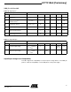
VDD_IO = 1.8V Table 8. Digital Inputs Logic Compatibility Name Parameter IIL Low level input current without pullup device(1) IIH CMOS Conditions Test Level VI = 0V High level input current without pull-down device(1) IIOZ Tri-state output leakage without pull-up/down device(1) VIL Min Typ Max Unit I 1 µA VI = VDD_IO I 1 µA VI = 0V or VDD_IO IV 1 µA Low level input voltage(1) I 0.4 VDD_IO(1) V VIH High level input voltage(1) I 0.
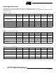
AT77C105A [Preliminary] VDD_IO = 2.3V to 3.6V Table 10. Digital Inputs Logic Compatibility CMOS Name Parameter Conditions Test Level IIL Low level input current without pullup device(1) VI = 0V IIH High level input current without pull-down device(1) IIOZ Tri-state output leakage without pull-up/down device(1) VIL Min Typ Max Unit I 1 µA VI = VDD_IO I 1 µA VI = 0V or VDD_IO IV 1 µA Low level input voltage(1) I 0.5 VDD_IO(1) V VIH High level input voltage(1) I 0.
Switching Performances The following characteristics are applicable to the operating temperature -40°C ≤ T ≤ +85°C. Typical conditions are: nominal value; Tamb = 25°C; FSCK = 12 MHz; duty cycle = 50%; CLOAD 120 pF in digital output unless specified otherwise. Table 12. Timings Parameter Symbol Test Level Min Clock frequency acquisition mode FACQ IV Clock frequency navigation mode and chip control FCTRL DC Duty cycle (clock SCK) Typ Max Unit 8 16 MHz I - 0.
AT77C105A [Preliminary] Table 15. 1.
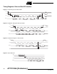
Timing Diagrams: Slow and Fast SPI Interface Figure 3. Read Timing Fast SPI Slave Mode RST SS Trstsu Tsssu Tsshd DC SCK Tdis Tv MISO Figure 4. Read/Write Timing Slow SPI Slave Mode SS Tsssu Tsshd SCK Tsu Th MOSI MISO Figure 5. Read Status Register to Release IRQ SS SCK 1 MOSI 1 0 0 0 0 X X Tirq IRQ Figure 6.
AT77C105A [Preliminary] Functional Description The AT77C105A is a fingerprint sensor based on FingerChip technology. It is controlled by an SPI serial interface through which output data is also transferred (a slow SPI for the pointing function and a fast one for acquisition). Six modes are implemented: – Sleep Mode: A very low consumption mode controlled by the reset pin RST. In this mode, the internal clocks are disabled and the registers are initialized.
Sensor and Block Diagram Figure 7.
AT77C105A [Preliminary] Function Registers Table 16.
Status Register Register Name: Status (8 bits) Access Type: Read Only Function: State of AT77C105A b7 b6 b5 b4 b3 b2 b1 b0 CLICK MOV TRANSIT SLICE READERR – – – 0 0 0 0 0 0 0 0 • CLICK: Click detection 0: default 1: click detected • MOV: Movement detection 0: default 1: X or Y movement detected • TRANSIT: Not used, for testing only • SLICE: Not used, for testing only • READERR: Read error detection 0: default, no error 1: read error detected Note: 14 To clear the interr
AT77C105A [Preliminary] Modectrl Register Register Name: Modectrl (7 bits) Access Type: Read/Write Function: Mode control b6 b5 b4 b3 b2 b1 b0 MODE (MSB) MODE MODE MODE (LSB) ANALOGRST – – 0 0 0 0 1 0 0 • MODE: Select operating mode 0000: standby 0001: test (reserved for factory use) 0010: click 0100: navigation 1000: acquisition Certain changes can be made. For example, MODE can be set to 0b0110 to activate click and navigation.
Enctrl Register Register Name: Enctrl (7 bits) Access Type: Read/Write Function: Interrupts control b6 CLICKEN 0 b5 MOVEN 0 b4 TRANSITEN 0 • b3 SLICEN 0 b2 READERREN 0 b1 – 0 b0 – 0 CLICKEN: Click interrupts enable 0: default 1: click IRQ enabled IRQ is generated when a click is detected. • MOVEN: Movement interrupts enable 0: default 1: movement IRQ enabled IRQ is generated when an X or Y movement is detected.
AT77C105A [Preliminary] 1: watchdog enabled Watchdog automatically stops heating of the sensor after a time-out. • HEATV (2 bits): Heating power value 00: 50 mW 01: 100 mW 10: reserved 11: reserved VDD is between 2.5 and 3.6V. Notes: Navctrl Register 1. Heating can only be used in the acquisition mode (it is not allowed in navigation or click modes). 2. The oscillator has to be activated when the watchdog is required and must not be stopped while the watchdog remains active.
Sets the minimum analog value detected as a high level (‘1’) and the maximum analog value detected as a low level (‘0’). See Note 3 on page 18. Notes: Clickctrl Register 1. Navfreq and Navv registers should not be changed once the navigation mode is selected. Finger sensitivity refers to the minimum level of information required from a finger. The sensitivity is linked to the integration time; a longer integration time enables better sensitivity but does not tolerate fast movement. 2.
AT77C105A [Preliminary] Two transitions are interpreted as a click if the number of slices between them is less than CLICKCPT. This is used to differentiate a touch-down/touch-up from a real click. A click is equivalent to two close touch-down/touch-up transitions. This register adjusts the “time out” for considering the two transitions as a click. Note: Movectrl Register Clickfreq and Clickcpt registers should not be changed once the click mode is selected.
Navigation Register Register Name: Navigation (3 x 8 bits) Access Type: Read Only (these three registers cannot be read individually. The reading command of the first navigation register [address 0b1000] returns the value of the three registers). Function: The format of the navigation registers is similar to the PS/2 protocol. Three registers are used to codemovements and clicks. The navigation registers are initialized after each reading. The registers only represent actions (movement, click, transition...
AT77C105A [Preliminary] Note: In the PS/2 protocol, bits b2 and b1 are used to code the middle and right buttons respectively, and b3 is set to high.
SPI Interface General Description Two communication busses are implemented in the device: • The control interface, a slow bus that controls and reads the internal registers (status, navigation, control...). • The pixels’ acquisition interface, a fast bus that enables full pixel acquisition by the host. A synchronous Serial Port Interface (SPI) has been adopted for the two communication busses. The SPI protocol is a slave/master fullduplex synchronous serial communication.
AT77C105A [Preliminary] Polarity configures the clock’s idle level, which is high (“1”) during polarity one of the operation and low (“0”) during polarity zero of the operation. AT77C105A and the SPI The AT77C105A is always the slave and the host always the master. The host drives the SCK clock. Both the AT77C105A and the host transmit data with the MISO signal. The word length of the transferred data is fixed to 8 bits. The Most Significant Bit (MSB) is sent first.
Control Interface (Slow SPI) This interface controls the sensor’s internal registers. The protocol enables reading and writing of these registers. The master (host) initiates transfers to the slave (sensor). The sensor can only use its interrupt pin to communicate with the host. When the host is interrupted, it must read the status register before continuing operation. The word length of the transferred data is fixed to 8 bits. The Most Significant Bit (MSB) is sent first.
AT77C105A [Preliminary] Communication Speed To reduce consumption, the control interface’s communication speed is set to the lowest possible speed and depends on the host’s configuration. To communicate with “fast” controllers, the sensor’s communication speed can be set to 200 kbits/s. Example for the MODECTRL Register Figure 10 represents a typical writing sequence into an internal register (MODECTRL register in this example). See Appendix B for flowchart. Figure 10.
Example of Navigation Registers Figure 12 represents a typical reading sequence of the three navigation registers. Refer to “Appendix C” on page 37 for flowchart Figure 12.
AT77C105A [Preliminary] Figure 13. Example of an 8-bit Access Controller FSS/ = 0 Sensor Sending of Dummy Data 0b0000000 Reception of 2 Pixels Sending of 2 Pixels (8 Bits) End of No Communication ? Yes FSS/ = 1 During an 8-bit access, the sensor transmits two pixels (each pixel is coded on 4 bits). Figure 14.
The first dummy column, at the beginning of the pixel array, is added to the sensor to act as a specific easy-to-detect pattern, and represents the start of the frame tag. The pixel array is always read in the following order: the first byte, following the 4 bytes of the dummy column, which contains the value of the pixels physically located on the upper left corner of the array, when looking at the die with bond pads to the right.
AT77C105A [Preliminary] Table 17.
Registration Integration Time The pixel’s integration time (the time needed for one frame reading) must be as regular as possible to obtain consistent fingerprint slices. This time is directly dependant on the SCK, SPI clock and frequency. Therefore, the SPI cycle of 4 × 8 × 233 clock pulses should be as regular as possible.µ Figure 17.
AT77C105A [Preliminary] Navigation See “Navigation Register” on page 20. The typical navigation slice frequency has been fixed to 2.9 kHz. A programmable divider is implemented in the control registers (NAVFREQ) to reduce this frequency. Finger displacement is provided as a number of pixels in X and Y directions. Negative movements are possible. The register is cleared after the navigation registers are read. These registers are incremented or decremented between two accesses. Table 18.
The dissipated die power is quasi constant over a significant supply voltage range as shown below (mode 50 mW selected): Figure 18. Power = f ( Vdd ) 5,40E-02 Power ( W ) 5,30E-02 5,20E-02 5,10E-02 5,00E-02 4,90E-02 4,80E-02 2 2,2 2,4 2,6 2,8 3 3,2 3,4 3,6 3,8 VDD Power = f ( Vdd) Note: This function is useless for navigation and click modes.
AT77C105A [Preliminary] Navigation and Click Modes Current Consumption Static Current Consumption The SPI bus’ consumption is very low in click and navigation modes, the majority of the consumption being generated by the analog part of the circuit. Therefore, the static and dynamic consumption is almost the same. Dynamic Current Consumption With a 30 pF load at maximum clock frequency, the current consumption in click mode is almost 300 µA on pins VDD.
Package Information Electrical Disturbances Three areas of the FingerChip device must never be in contact with the casing, or any other component, so as to avoid electrical disturbances. These areas are shown in Figure 21: Figure 21. Sensitive Areas 6 mm 11.5 mm Figure 22. Epoxy Overflow Maximum epoxy overflow width: 0.35 mm on the die edge. Maximum epoxy overflow thickness: 0.33 mm. 0.35 0.33 AA Section Fingerchip Note: Epoxy Glue Overflow Refer to Figure 19 on page 33.
AT77C105A [Preliminary] Appendix A Controller Initialization Host Controller Initialization Controller Initialized ? No Yes SPI Initialization (Phase = 0, Polarity = 1) SPI Initialized ? No Yes RST = 1 Sensor Initialization Pulse > 10 us ? No Yes RST = 0 35 5419A–BIOM–01/05
Appendix B Example for the MODECTRL Register Controller Sensor Reception of the Command Reading of MODECTRL Interrupts Masked SSS/ = 0 MODECTRL Reading Requested Sending 0b11000100 No Transfer Ended ? Yes Sending of MODECTRL Modification of MODECTRL to Change Mode Bits Transfer Ended ? No Yes Modification of MODECTRL to Change Mode Bits Reception of the Command Writing of MODECTRL MODECTRL Writing Requested Sending of 0b10000100 No Transfer ended ? Yes Reception of MODECTRL Sending of the Ne
AT77C105A [Preliminary] Appendix C Example of Navigation Registers Controller Sensor Reception of the Command Reading of NAVIGATION Interrupts Masked SSS/ = 0 NAVIGATION Reading Requested Sending 0b11000000 No Transfer Ended ? Yes Sending of NAVIG1 Sending of Dummy Data 0b00000000 Reception of NAVIG1 No Transfer Ended ? Yes Sending of NAVIG2 Sending of Dummy Data 0b00000000 Reception of NAVIG2 Transfer Ended ? No Yes Sending of NAVIG3 Sending of Dummy Data 0b00000000 Reception of NAVIG3 No
Appendix D Example of an Interrupt Generated by a Movement Detection Controller Main Program Sensor Interrupt Generated IRQ/ = 0 Interrup ? No Interrupts Masked SSS/ = 0 Reception of the Command STATUS Reading Requested Sending of 0b11000000 No Transfer Ended ? Yes Sending of STATUS Interrupts Cleared Sending of Dummy Data 0b00000000 Reception of STATUS Transfer Ended ? No Yes Interrupts Control Detection of Movement Reception of the Command Reading of NAVIGATION NAVIGATION Reading Requested
Atmel Corporation 2325 Orchard Parkway San Jose, CA 95131, USA Tel: 1(408) 441-0311 Fax: 1(408) 487-2600 Regional Headquarters Europe Atmel Sarl Route des Arsenaux 41 Case Postale 80 CH-1705 Fribourg Switzerland Tel: (41) 26-426-5555 Fax: (41) 26-426-5500 Asia Room 1219 Chinachem Golden Plaza 77 Mody Road Tsimshatsui East Kowloon Hong Kong Tel: (852) 2721-9778 Fax: (852) 2722-1369 Japan 9F, Tonetsu Shinkawa Bldg.