Features • Fully Integrated 2.4 GHz-band Transceiver • -101 dBm Receiver Sensitivity • Low Current Consumption (Typical Values) − SLEEP = 0.1 µA − TRX_OFF = 1.7 mA − RX_ON = 16 mA − BUSY_TX = 17 mA (max. PTX) • Power Supply Range 1.8V – 3.6V − Internal LDO Voltage Regulators − Battery Monitor • SPI Slave Interface • Baseband Signal Processing Compliant with IEEE 802.15.
Table of contents 1. 2. 3. Abbreviations ...................................................................................................................................................4 General Circuit Description..............................................................................................................................5 Technical Parameters......................................................................................................................................6 3.1.
AT86RF230 8. 9. 10. 10.1. 10.2. 10.3. 10.4. 10.5. 11. 12. 13. 14. 15. 16. Control Registers ...........................................................................................................................................31 Application Circuit ..........................................................................................................................................42 Pin Configuration .................................................................................................
1.
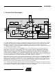
AT86RF230 XTAL2 XTAL1 2. General Circuit Description Analog Domain AVREG BATMON FTN Digital Domain DCLK TX power control XOSC DVREG IRQ PA Frequency Synthesis TX Data SEL TX BBP MISO RFP SPI Slave Interface Control Logic/ Configuration Registers RFN MOSI I LNA PPF SCLK BPF Limiter ADC RX BBP TRX Data Buffer Q CLKM RSSI AGC SLP_TR 5 RSTN Figure 2-1.
3. Technical Parameters 3.1. Absolute Maximum Ratings Note: Stresses beyond those listed under “Absolute Maximum Ratings” may cause permanent damage to the device. This is a stress rating only and functional operation of the device at these or any other conditions beyond those indicated in the operational sections of this specifications is not implied. Exposure to absolute maximum rating conditions for extended periods may affect device reliability. No Parameter Symbol Min -50 3.1.
AT86RF230 No 3.3.5 Parameter Controller clock frequency (CLKM) Table 3-3. Symbol Min fCLKM Typ Max 0 1 2 4 8 16 Unit Conditions/Notes MHz MHz MHz MHz MHz MHz Programmable in register TRX_CTRL_0 Digital Pin Specifications The capacitive load should not be larger than 50 pF for all I/Os when using the default driver strength settings. Generally, large load capacitances will increase the overall current consumption. 3.4.
No 3.5.7 Parameter Min Typ Spurious emissions 30 – ≤1000 MHz >1 – 12.75 GHz 1.8 – 1.9 GHz 5.15 – 5.3 GHz Table 3-5. 3.6. Symbol Max Unit Conditions/Notes -36 -30 -47 -47 dBm dBm dBm dBm Complies with EN 300 440, FCC-CFR-47 part 15, ARIB STD-66, RSS-210 TX Parameters Receiver Specifications Test Conditions (unless otherwise stated): Vdd = 3V, f = 2.
AT86RF230 3.7. Current Consumption Specifications Test Conditions (unless otherwise stated): Vdd = 3V, Tamb = 25°C, CLKM = OFF, Measurement setup see Figure 9-1 No Parameter Symbol 3.7.1 Supply current transmit mode IBUSY_TX 3.7.2 Supply current receive mode 3.7.3 Supply current TRX_OFF mode 3.7.4 Supply current SLEEP mode Table 3-7. 3.8.
3.9. No Crystal Parameter Specifications Parameter Symbol 3.9.1 Crystal frequency f0 3.9.2 Load capacitance CL 3.9.3 Static capacitance 3.9.4 Series resistance Table 3-9.
AT86RF230 4. Basic Operating Modes This section summarizes all features that are needed to provide the basic functionality of a transceiver system, such as receiving and transmitting frames, and powering down. These basic operating modes are sufficient for ZigBee applications and are shown in Figure 4-1.
The state change commands FORCE_TRX_OFF and TRX_OFF both lead to a transition into TRX_OFF state. If the transceiver is in the BUSY_RX or BUSY_TX state, the command FORCE_TRX_OFF interrupts the active receiving or transmitting process, and forces an immediate transition. On the other hand, a TRX_OFF command is stored until a frame currently being received or transmitted is finished. After the end of the frame, the transition to TRX_OFF is performed. 4.2. 4.2.1.
AT86RF230 4.2.5. RX_ON and BUSY_RX The RX_ON mode enables the analog and digital receiver blocks and the PLL frequency synthesizer. The transition from TRX_OFF mode to RX_ON mode is started by setting the TRX_STATE to RX_ON via a SPI write access to register 0x02 (TRX_STATE). The receive mode is internally divided into RX_ON mode and BUSY_RX mode. There is no difference between the modes with respect to the analog radio part.
micro-controller. An additional 256 µs timer ensures that frequency stability is sufficient to drive filter tuning (FTN) and the PLL. After band-gap voltage and digital voltage regulator settling, the transceiver enters the TRX_OFF state and waits for further commands.
AT86RF230 4.3.3. State Transition Timing The transition numbers correspond to Figure 4-1 and do not include SPI access time if not otherwise stated. See measurement setup in Figure 9-1.
5. Extended Operating Modes The AT86RF230 transceiver implements address filtering, automatic acknowledgement frame generation and automatic frame retransmission for peer-to-peer networks in compliance with the IEEE 802.15.4 standard. Automatic modes help to achieve low power consumption and low peak current: TX-ARET (transmit/auto-retry) and RX-AACK (receive/auto-acknowledge).
AT86RF230 SLEEP (Sleep Mode) XOSC=ON Pull=ON XOSC=OFF Pull=OFF F OF X_ TR FORCE_TRX_OFF 1 SL P_ TR SL =0 P_ TR =1 P_ON (Power-on after VDD) 2 TRX_OFF 12 13 (Clock Mode) (all modes except SLEEP) 3 RST=0 (all modes except P_ON) 8 RX_ON (Rx Listen Mode) ON T_ BUSY_RX_ AACK_NOCLK RX_AACK_ON Frame Start RX_AACK_ ON_NOCLK (Auto Acknowledge) Frame (Auto Acknowledge) Rejected Figure 5-1.
5.2. Configuration The initialization of the AT86RF230 prior to using RX-AACK or the TX-ARET mode is similar to initializing the IC prior to switching to regular RX or TX modes. RX_AACK_ON mode is enabled after the register bits TRX_CMD in register 0x02 (TRX_STATE) is written using RX_AACK_ON. The IC is in the RX_AACK_ON mode when the register 0x01 (TRX_STATUS) changes to RX_AACK_ON or BUSY_RX_AACK. For correct RX_AACK_ON operation, the register bit TX_AUTO_CRC_ON (register 0x05) must be set to “1”.
AT86RF230 even after the maximum number of retries, it will abort the transaction, raise the TRX_END interrupt, and set the value of the TRAC_STATUS register bits to CHANNEL_ACCESS_FAILURE. Upon the detection of a clear channel, the transceiver starts the frame transmission. It parses the frame as it is transmitted to check if an ACK reply will be expected. If no ACK is expected, the transceiver will raise an interrupt after the frame transmission completes.
6. Functional Description 6.1. RSSI/Energy Detection The internal limiter amplifier provides an RSSI value which reflects the current receive signal strength at the antenna pin of the AT86RF230. The RSSI is a 5-bit value indicating the receive power in steps of 3 dB (see register 0x06), and is updated every 2 µs. The receiver ED measurement is used with the channel-scan algorithm. An ED request (write access to register 0x07) as defined by the IEEE 802.15.4 standard has a measurement time of 128 µs.
AT86RF230 range from 400 nF to 10 µF. A higher capacitor value provides better voltage stability, but increases the voltage regulator settling time. VDD Bandgap voltage reference 1.25V VDEC VREG_TRIM[1:0] Figure 6-1. Simplified Schematic of VREG The voltage regulators can be configured using the register 0x10 (VREG_CTRL). The read-only bit values AVDD_OK = 1 and DVDD_OK = 1 indicate a stable, regulated supply voltage.
The BATMON can be configured using the register 0x11 (BATMON). BATMON_VTH[3:0] sets the threshold voltage. It is programmable with a resolution of 75 mV in the upper voltage range (BATMON_HR = 1) and with a resolution of 50 mV in the lower voltage range (BATMON_HR = 0).
AT86RF230 VDD XTAL_TRIM[3:0] CTRIM XTAL_TRIM[3:0] CTRIM AT86RF230 XTAL2 CPAR Figure 6-3. 16MHz CX XTAL1 PCB CPAR CX Simplified XOSC Schematic with External Components When using an external reference frequency, the signal needs to be connected to pin XTAL1 as indicated in Figure 6-4 and the register bits XTAL_MODE needs to be set to the external oscillator mode. The oscillation amplitude shouldn’t be larger than 500 mV, peak-to-peak. AT86RF230 XTAL2 XTAL1 PCB 16 MHz Figure 6-4. 6.7.
Both calibration routines will be initiated automatically when the PLL is turned on. Additionally, the center frequency calibration is running when the PLL is programmed to a different channel (register 0x08 bits [4:0]). If the PLL is not turned off for a long time, the control loops should be manually initiated from time to time. The calibration interval depends on environment temperature variations but should not be longer than 5 min. 6.8.
AT86RF230 7. PHY to Micro-Controller Interface In the following paragraphs, the PHY to micro-controller interface is defined. The SPI protocol and timing access are shown, as well as buffer access modes with examples. Controllers with an SPI interface such as an AVR will work with the AT86RF230 interface. The SPI interface is used for both register programming as well as for frame transfer. The additional control signals are connected to the GPIO interface of the controller.
The interface is designed to work in synchronous or asynchronous mode. In synchronous mode, the CLKM output of the transceiver IC is used as the master clock of the controller. The SPI clock can be any integer-divided clock ratio up to 8 MHz. Nevertheless, usage of an independent controller clock for an asynchronous interface is possible. In asynchronous mode, the maximum SPI clock speed is limited to 7.5 MHz. The external CLKM output signal is not required and can be disabled.
AT86RF230 Write Register Access Read Register Access CLKM SEL SCLK MOSI COMMAND MISO WRITE DATA XX XX XX XX Figure 7-4. 7.3. COMMAND READ DATA SPI Register Access Sequence Frame Buffer Access Modes (Long Modes) These modes are used to upload or download frames as well as access the frame buffer directly. Each transfer starts with a control byte. If this byte indicates a frame upload or download, the next byte indicates the frame length followed by the PSDU data.
7.4. Frame Receive Procedure The following transactions are required to receive a frame over the SPI: Controller IRQ issued PHY read IRQ status register (register access) IRQ line deasserted receiving frame data (frame receive mode) Figure 7-8.
AT86RF230 CLKM Frame_download SEL SCLK MOSI COMMAND FRAME LENGTH XX MISO XX FRAME DATA 1 XX FRAME DATA 2 XX FRAME DATA 3 XX FRAME DATA n XX IRQ Transmit Start SLP_TR Figure 7-11. 7.6. Frame Transmit Sequence (SLP_TR Assertion Starts Transmission) Sleep/Wake-up and Transmit Signal The SLP_TR signal is a multi-functional pin. It can be used as transmit start or as a sleep signal. The function of the pin depends on the transceiver status.
CLKM async timer (controller) elapsed 35 main clock cycles SLP_TR Figure 7-12. Sleep and Wake-up Initiated by Asynchronous Controller Timer Output CLKM 35 main clock cycles SLP_TR transceiver IRQ issued IRQ Figure 7-13. 7.7. Wake-up Initiated by Transceiver Interrupt Interrupt Logic The AT86RF230 can differentiate between six interrupt events. Each interrupt can be enabled or disabled by writing the corresponding bit to the interrupt mask register.
AT86RF230 8. Control Registers The AT86RF230 provides a register space of 64 8-bit registers, which is used to configure the IC as well as to store signaling information read by the firmware. Note that all registers not mentioned within the following table are reserved for internal use and must not be written to. When writing to a non-reserved register, any individual bits of that register marked as reserved can only be overwritten by their reset value. Reg.-Addr.
Reg.-Addr. Register Name Description 0x29 IEEE_ADDR_5 Current node IEEE address for address recognition 0x2A IEEE_ADDR_6 Current node IEEE address for address recognition 0x2B IEEE_ADDR_7 Current node IEEE address for address recognition 0x2C XAH_CTRL 0x2D CSMA_SEED_0 CSMA seed value 0x2E CSMA_SEED_1 CSMA seed value Table 8-1.
AT86RF230 Bit Field Name Reset R/W 7:5 TRAC_STATUS 0 R 4:0 TRX_CMD 0 R/W Table 8-3. Note: Comments 3’d0: SUCCESS 3’d3: CHANNEL_ACCESS_FAILURE 3’d5: NO_ACK All other values are reserved. Transceiver control commands: 5’d0: NOP 5’d2: TX_START 5’d3: FORCE_TRX_OFF 5’d6: RX_ON 5’d8: TRX_OFF (CLK Mode) 5’d9: PLL_ON (TX_ON) 5’d22: RX_AACK_ON 5’d25: TX_ARET_ON All other values are mapped to NOP. 0x02 - TRX_STATE TRX_CMD = “0” after power on reset (POR).
Bit Field Name 7 TX_AUTO_CRC_ON Reset R/W Comments 0 R/W AUTO_CRC mode: 1’d0: disable 1’d1: enable 0 R 0 R/W 6:4 3:0 TX_PWR Table 8-5. Bit Field Name 34 TX Power Setting Output Power [dBm] 0 3.0 1 2.6 2 2.1 3 1.6 4 1.1 5 0.5 6 -0.2 7 -1.2 8 -2.2 9 -3.2 10 -4.2 11 -5.2 12 -7.2 13 -9.2 14 -12.2 15 -17.
AT86RF230 Bit Field Name Reset R/W 7:0 ED_LEVEL 0 R Table 8-7. Note: Comments ED level for current channel. The min. ED value (0) indicates receiver power less than or equal to -91 dBm. The range is 84 dB with a resolution of 1 dB and an absolute accuracy of ±5 dB. 0x07 - PHY_ED_LEVEL A write access initiates the ED measurement (ED.request). Bit Field Name Reset R/W Comments 7 CCA_REQUEST 0 R/W 1’d1: starts a CCA check (CCA.
Bit Field Name Reset R/W Comments 7:4 CCA_CS_THRES 12 R/W Threshold for CCA_CS 3:0 CCA_ED_THRES 7 R/W An ED value above the threshold signals a busy channel during a CCA_ED measurement. Table 8-9. Note: 0x09 - CCA_THRES CCA_ED_THRES: The CCA_ED request will indicate a busy channel, if the measured receive power is above -91 dBm + 2*CCA_ED_THRES[dB]. Bit Field Name Reset R/W Comments 7:0 IRQ_MASK 255 R/W Mask register for IRQs. If bit is set to high, then the IRQ is enabled.
AT86RF230 Bit Field Name Reset R/W Comments 3 DVREG_EXT 0 R/W 1’d0: 1’d1: use internal digital voltage regulator use external voltage regulator 2 DVDD_OK 0 R 1’d0: 1’d1: digital voltage regulator is disabled internal digital voltage is correct and stable 1:0 DVREG_TRIM 0 R/W Controls the voltage of the digital voltage regulator. 2’d0: 1.80V 2’d1: 1.75V 2’d2: 1.84V 2’d3: 1.
Bit Field Name Reset R/W Comments 7:4 XTAL_MODE 15 R/W XTAL Modes: 4’d0: switch off 4’d4: external oscillator 4’d15: internal oscillator All other modes are reserved and should not be used. 3:0 XTAL_TRIM 0 R/W Binary coded capacitance array for XTAL trimming. Values: 0 pF, 0.3 pF, …, 4.8 pF Table 8-14.
AT86RF230 Bit Field Name Reset R/W 7:0 MAN_ID_0 31 R Table 8-20.
Bit Field Name 7:0 IEEE_ADDR_3 Table 8-29.
AT86RF230 Bit Field Name 7:6 MIN_BE 5:4 Reset R/W Comments 3 R/W Minimum back-off exponent in the CSMA/CA algorithm. 0 R Reserved 3 I_AM_COORD 0 R/W Use for address filtering within AACK mode (PAN coordinator) 1’d0: disable 1’d1: enable 2:0 CSMA_SEED_1 2 R/W Higher 3 bits of CSMA_SEED, bits[10:8] Seed for the random number generator in the CSMA/CA algorithm Table 8-36.
9. Application Circuit An application circuit with a single-ended RF connector is shown in Figure 9-1. An SMD-balun transforms the 100Ω differential RF inputs/outputs of the AT86RF230 to a 50Ω single ended RF port. The capacitors C1 and C2 form a DC-block. Power supply decoupling capacitors (CB2, CB4) are connected to the analog (28) and the digital supply pin (15). Capacitors CB1 and CB3 are load capacitors for the analog and digital voltage regulators.
AT86RF230 Vdd CB2 CX1 CX2 XTAL 31 30 29 28 27 26 25 GND GND VDEC2 VDD GND XTAL2 XTAL1 1 GND C1 RF 2 GND SEL 23 3 GND MOSI 22 4 RFP B1 GND 21 AT86RF230 5 RFN MISO 20 VDEC1 VDEC1 VDD GND GND 18 GND 7 GND SLP_TR SCLK 19 GND 6 GND GND C2 IRQ 24 9 10 11 12 13 14 15 16 8 RST CB3 Figure 9-1.
10.
AT86RF230 GND GND GND VDEC2 VDD GND XTAL2 XTAL1 10.1. Pin-out Diagram 1 2 3 4 5 6 7 8 32 31 30 29 28 27 26 25 24 23 22 21 AT86RF230 20 19 18 17 9 10 11 12 13 14 15 16 IRQ SEL MOSI GND MISO SCLK GND CLKM GND GND SLP_TR GND VDEC1 VDEC1 VDD GND GND GND GND RFP RFN GND GND RST 10.2. Decoupling Correct functionality requires de-coupling of the internal power supply voltage (VDEC1/2).
RFP RFN 0.9V M0 Figure 10-1. LNA RX PA TX CM Feedback RXTX Simplified RF Front-end Schematic A simplified schematic of the RF front end is shown in Figure 10-1. RF port DC values depend on the operating mode. In TRX_OFF mode, the RF pins are pulled to ground, preventing a floating voltage larger than 1.8V which is not allowed for the internal circuitry. In receive mode, the RF input provides a low-impedance path to ground when transistor M0 pulls the inductor center tap to ground.
AT86RF230 11. Ordering Information Ordering Code Package Voltage Range AT86RF230-ZU QN 1.8 – 3.6V Package Type QN Temperature Range Industrial (-40°C to 85°C) Lead-free/Halogen-free Description 32QN1, 32-lead 5.0 x5.0mm Body, 0.50mm Pitch, Quad Flat No-lead Package (QFN) Sawn Note: T&R quantity 2,500. Please contact your local Atmel sales office for more detailed ordering information and minimum quantities. 12.
14. Package Drawing – 32QN1 D A A3 E Pin 1 Corner A1 A2 Top View Side View Pin 1 Corner COMMON DIMENSIONS (Unit of Measure = mm) SYMBOL D2 MIN D E e E2 L E2 1.25 A 0.80 0.90 1.00 A1 0.0 0.02 0.05 A2 0.0 0.65 1.00 L Notes: b NOTE 5.00 BSC 1.25 3.25 3.25 0.20 REF 0.30 e Bottom View MAX D2 A3 b NOM 5.00 BSC 0.40 0.50 0.50 BSC 0.18 0.23 0.30 2 1. This drawing is for general information only.
AT86RF230 15. [1] [2] [3] [4] 16. References IEEE Std 802.15.4-2003: Wireless Medium Access Control (MAC) and Physical Layer (PHY) Specifications for Low-Rate Wireless Personal Area Networks (LR-WPANs) ANSI / ESD-STM5.1-2001: ESD Association Standard Test Method for electrostatic discharge sensitivity testing – Human Body Model (HBM) EIA / JESD22-A115-A: Electronic Industries Association, Electrostatic Discharge Sensitivity Testing – Machine Model (MM) ESD-STM5.3.
Atmel Corporation 2325 Orchard Parkway San Jose, CA 95131, USA Tel: 1(408) 441-0311 Fax: 1(408) 487-2600 Regional Headquarters Europe Atmel Sarl Route des Arsenaux 41 Case Postale 80 CH-1705 Fribourg Switzerland Tel: (41) 26-426-5555 Fax: (41) 26-426-5500 Atmel Operations Memory RF/Automotive 2325 Orchard Parkway San Jose, CA 95131, USA Tel: 1(408) 441-0311 Fax: 1(408) 436-4314 Microcontrollers 2325 Orchard Parkway San Jose, CA 95131, USA Tel: 1(408) 441-0311 Fax: 1(408) 436-4314 La Chantrerie BP 70602