Features • High Performance RF-CMOS 2.4 GHz Radio Transceiver Targeted for IEEE 802.15.4™, ZigBee™ and ISM Applications • Industry Leading Link Budget (104 dB) – Receiver Sensitivity -101 dBm – Programmable Output Power from -17 dBm up to +3 dBm • Ultra-Low Current Consumption: – SLEEP = 0.02 µA – TRX_OFF = 0.4 mA – RX_ON = 13.2 mA – BUSY_TX = 14.3 mA (at max. Transmit Power of +3 dBm) • Ultra-Low Supply Voltage (1.8V to 3.
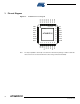
1. Pin-out Diagram D IG 3 1 D IG 4 2 AVSS 3 R FP 4 R FN 5 AVSS 2 X TA L 2 X TA L 1 AVSS E V DD A V DD AVSS 32 31 30 29 28 27 26 25 24 exposed paddle IR Q /SEL 22 M OSI 21 D VSS 20 M IS O 6 19 SC LK D VSS 7 18 D VSS /R S T 8 17 9 10 11 12 13 14 15 16 C LKM DE V D D DV D D DV D D D VSS DI G 2 S L P _ TR A T86 R F2 3 1 D VSS 23 AVSS DI G 1 Note: AVSS AT86RF231 Pin-out Diagram AVSS Figure 1-1.
AT86RF231 1.1 Pin Descriptions Table 1-1. Pin Description AT86RF231 Pins Name Type Description 1 DIG3 Digital output (Ground) 1. RX/TX Indicator, see Section 11.5 2. If disabled, pull-down enabled (AVSS) 2 DIG4 Digital output (Ground) 1. RX/TX indicator (DIG3 inverted), see Section 11.5 2.
Table 1-1. 4 Pin Description AT86RF231 (Continued) Pins Name Type Description 29 AVDD Supply Regulated 1.8V voltage regulator; analog domain, see Section 9.
AT86RF231 1.2 1.2.1 Analog and RF Pins Supply and Ground Pins EVDD, DEVDD EVDD and DEVDD are analog and digital supply voltage pins of the AT86RF231 radio transceiver. AVDD, DVDD AVDD and DVDD are outputs of the internal 1.8V voltage regulators. The voltage regulators are controlled independently by the radio transceivers state machine and are activated dependent on the current radio transceiver state. The voltage regulators can be configured for external supply. For details, refer to Section 9.
The RF port DC values depend on the operating state, refer to Section 7. “Operating Modes” on page 33. In TRX_OFF state, when the analog front-end is disabled (see Section 7.1.2.3 “TRX_OFF Clock State” on page 35), the RF pins are pulled to ground, preventing a floating voltage. In transmit mode, a control loop provides a common-mode voltage of 0.9V. Transistor M0 is off, allowing the PA to set the common-mode voltage.
AT86RF231 1.3 Digital Pins The AT86RF231 provides a digital microcontroller interface. The interface comprises a slave SPI (/SEL, SCLK, MOSI and MISO) and additional control signals (CLKM, IRQ, SLP_TR, /RST and DIG2). The microcontroller interface is described in detail in Section 6. “Microcontroller Interface” on page 16. Additional digital output signals DIG1...DIG4 are provided to control external blocks, i.e. for Antenna Diversity RF switch control or as an RX/TX Indicator, see Section 11.
1.3.3 Register Description Register 0x03 (TRX_CTRL_0): The TRX_CTRL_0 register controls the drive current of the digital output pads and the CLKM clock rate. Bit 7 6 5 PAD_IO 4 PAD_IO_CLKM 3 2 CLKM_SHA_SEL 1 0 CLKM_CTRL TRX_CTRL_0 Read/Write R/W R/W R/W R/W R/W R/W R/W R/W Initial Value 0 0 0 1 1 0 0 1 • Bit [7:6] - PAD_IO The register bits set the output driver current of all digital output pads, except CLKM. Table 1-5.
AT86RF231 2. Disclaimer Typical values contained in this datasheet are based on simulations and testing. Min and Max values are available when the radio transceiver has been fully characterized. 3. Overview The AT86RF231 is a feature rich, low-power 2.4 GHz radio transceiver designed for industrial and consumer ZigBee/IEEE 802.15.4 and high data rate 2.4 GHz ISM band applications. The radio transceiver is a true SPI-to-antenna solution.
4. General Circuit Description This single-chip radio transceiver provides a complete radio transceiver interface between an antenna and a microcontroller. It comprises the analog radio, digital modulation and demodulation including time and frequency synchronization and data buffering. The number of external components is minimized such that only the antenna, the crystal and decoupling capacitors are required.
AT86RF231 An internal 128-byte RAM for RX and TX (Frame Buffer) buffers the data to be transmitted or the received data. The configuration of the AT86RF231, reading and writing of Frame Buffer is controlled by the SPI interface and additional control lines. The AT86RF231 further contains comprehensive hardware-MAC support (Extended Operating Mode) and a security engine (AES) to improve the overall system power efficiency and timing.
5. Application Circuits 5.1 Basic Application Schematic A basic application schematic of the AT86RF231 with a single-ended RF connector is shown in Figure 5-1 on page 12. The 50Ω single-ended RF input is transformed to the 100Ω differential RF port impedance using balun B1. The capacitors C1 and C2 provide AC coupling of the RF input to the RF port, capacitor C4 improve matching. Figure 5-1.
AT86RF231 the reference frequency, large parasitic capacitances should be avoided. Crystal lines should be routed as short as possible and not in proximity of digital I/O signals. This is especially required for the High Data Rate Modes, refer to Section 11.3 “High Data Rate Modes” on page 137. Crosstalk from digital signals on the crystal pins or the RF pins can degrade the system performance.
5.2 Extended Feature Set Application Schematic The AT86RF231 supports additional features like: • Security Module (AES) see Section 11.1 • High Data Rate Mode see Section 11.3 • Antenna Diversity uses pins DIG1/2 see Section 11.4 • RX/TX indicator uses pins DIG3/4 see Section 11.5 • RX Frame Time Stamp uses pin DIG2 see Section 11.6 An extended feature set application schematic illustrating the use of the AT86RF231 Extended Feature Set, see Section 11.
AT86RF231 control pins DIG1/DIG2, the RF signal is amplified by an optional low-noise amplifier (N2) and fed to the radio transceiver using the second RX/TX switch (SW1). During transmit the AT86RF231 TX signal is amplified using an external PA (N1) and fed to the antennas via an RF switch (SW2). In this example RF switch SW2 further supports Antenna Diversity controlled by the differential pin pair DIG1/DIG2. The security engine (AES) and High Data Rate Modes do not require specific circuitry to operate.
6. Microcontroller Interface This section describes the AT86RF231 to microcontroller interface. The interface comprises a slave SPI and additional control signals; see Figure 6-1 on page 16. The SPI timing and protocol are described below. Microcontroller to AT86RF231 Interface SPI AT86RF231 /SEL /SEL /SEL MOSI MOSI MOSI MISO MISO MISO SCLK SCLK SCLK GPIO1/CLK CLKM CLKM GPIO2/IRQ IRQ SPI - Master Microcontroller SPI - Slave Figure 6-1.
AT86RF231 Table 6-1. 6.1 Signal Description of Microcontroller Interface (Continued) SLP_TR Multipurpose control signal (functionality is state dependent, see Section 6.5): -Sleep/Wakeup enable/disable SLEEP state -TX start BUSY_TX_(ARET) state -disable/enable CLKM RX_(AACK)_ON state /RST AT86RF231 reset signal, active low DIG2 Optional, IRQ_2 (RX_START) for RX Frame Time Stamping, see Section 11.6 SPI Timing Description Pin 17 (CLKM) can be used as a microcontroller master clock source.
The SPI is based on a byte-oriented protocol and is always a bidirectional communication between master and slave. The SPI master starts the transfer by asserting /SEL = L. Then the master generates eight SPI clock cycles to transfer one byte to the radio transceiver (via MOSI). At the same time, the slave transmits one byte to the master (via MISO). When the master wants to receive one byte of data from the slave it must also transmit one byte to the slave. All bytes are transferred with MSB first.
AT86RF231 6.2 SPI Protocol Each SPI sequence starts with transferring a command byte from the SPI master via MOSI (see Table 6-2 on page 19) with MSB first. This command byte defines the SPI access mode and additional mode-dependent information. Table 6-2.
Figure 6-5. Packet Structure - Register Write Access byte 1 (command byte) MOSI 1 1 MISO ADDRESS[5:0] byte 2 (data byte) WRITE DATA[7:0] PHY_STATUS XX Each register access must be terminated by setting /SEL = H. Figure 6-6 on page 20 illustrates a typical SPI sequence for a register access sequence for write and read respectively. Figure 6-6. Example SPI Sequence - Register Access Mode Register Write Access Register Read Access /SEL SCLK MOSI WRITE COMMAND MISO PHY_STATUS 6.2.
AT86RF231 Note, the Frame Buffer read access can be terminated at any time without any consequences by setting /SEL = H, e.g. after reading the PHR byte only. On Frame Buffer write access the second byte transferred on MOSI contains the frame length (PHR field) followed by the payload data (PSDU) as shown by Figure 6-8 on page 21. Figure 6-8.
Figure 6-10. Example SPI Sequence - Frame Buffer Write of a Frame with 4 byte PSDU /SEL SCLK MOSI COMMAND MISO PHY_STATUS PHR PSDU 1 XX XX PSDU 2 XX PSDU 3 PSDU 4 XX XX Access violations during a Frame Buffer read or write access are indicated by interrupt IRQ_6 (TRX_UR). For further details, refer to Section 9.3 “Frame Buffer” on page 107. Notes • The Frame Buffer is shared between RX and TX; therefore, the frame data are overwritten by new incoming frames.
AT86RF231 On SRAM write access, one or more bytes of write data are transferred on MOSI starting with the third byte of the access sequence (see Figure 6-12 on page 23). On SRAM read or write accesses do not attempt to read or write bytes beyond the SRAM buffer size. Figure 6-12.
6.3 Radio Transceiver Status information Each SPI access can be configured to return status information of the radio transceiver (PHY_STATUS) to the microcontroller using the first byte of the data transferred via MISO. The content of the radio transceiver status information can be configured using register bits SPI_CMD_MODE (register 0x04, TRX_CTRL_1). After reset, the content on the first byte send on MISO to the microcontroller is set to 0x00. 6.3.
AT86RF231 6.4 Radio Transceiver Identification The AT86RF231 can be identified by four registers. One register contains a unique part number and one register the corresponding version number. Two additional registers contain the JEDEC manufacture ID. 6.4.
Table 6-6. JEDEC Manufacturer ID - Bits [7:0] Register Bit Value Description MAN_ID_0 0x1F Atmel JEDEC manufacturer ID, Bits [7:0] of 32 bit manufacturer ID: 00 00 00 1F Register 0x1F (MAN_ID_1): Bit 7 6 5 Read/Write R R R R Reset Value 0 0 0 0 +0x1F 4 3 2 1 0 R R R R 0 0 0 0 MAN_ID_1[7:0] MAN_ID_1 • Bit [7:0] - MAN_ID_1 Bits [15:8] of the 32-bit JEDEC manufacturer ID are stored in register bits MAN_ID_1. Bits [7:0] are stored in register 0x1E (MAN_ID_0).
AT86RF231 6.5 Sleep/Wake-up and Transmit Signal (SLP_TR) Pin 11 (SLP_TR) is a multi-functional pin. Its function relates to the current state of the AT86RF231 and is summarized in Table 6-8 on page 27. The radio transceiver states are explained in detail Section 7. “Operating Modes” on page 33. Table 6-8.
Figure 6-15. Sleep and Wake-up Initiated by Asynchronous Microcontroller Timer SLP_TR tTR2 CLKM 35 CLKM clock cycles CLKM off async timer elapses (microcontroller) Note: Timing figure tTR2 refer to section Table 7-1 on page 42. RX_ON and RX_AACK_ON states For synchronous systems, where CLKM is used as a microcontroller clock source and the SPI master clock (SCLK) is directly derived from CLKM, the AT86RF231 supports an additional power-down mode for receive operating states (RX_ON and RX_AACK_ON).
AT86RF231 6.6 Interrupt Logic 6.6.1 Overview The AT86RF231 differentiates between nine interrupt events (eight physical interrupt registers, one shared by two functions). Each interrupt is enabled by setting the corresponding bit in the interrupt mask register 0x0E (IRQ_MASK). Internally, each pending interrupt is stored in a separate bit of the interrupt status register. All interrupt events are OR-combined to a single external interrupt signal (IRQ, pin 24).
Note that AWAKE_END interrupt can usually not be seen when the transceiver enters TRX_OFF state after RESET, because register 0x0E (IRQ_MASK) is reset to mask all interrupts. In this case, state TRX_OFF is normally entered before the microcontroller could modify the register. The interrupt handling in Extended Operating Mode is described in Section 7.2.5 “Interrupt Handling” on page 67.
AT86RF231 Register 0x04 (TRX_CTRL_1): The TRX_CTRL_1 register is a multi purpose register to control various operating modes and settings of the radio transceiver. Bit 7 6 5 4 PA_EXT_EN IRQ_2_EXT_EN TX_AUTO_CRC_ON RX_BL_CTRL Read/Write R/W R/W R/W R/W R/W Reset Value 0 0 1 0 0 +0x04 3 2 1 0 IRQ_MASK_MODE IRQ_POLARITY R/W R/W R/W 0 0 0 SPI_CMD_MODE TRX_CTRL_1 • Bit 7 - PA_EXT_EN Refer to Section 11.5 “RX/TX Indicator” on page 147.
• Bit 0 - IRQ_POLARITY The default polarity of the IRQ pin is active high. The polarity can be configured to active low via register bit IRQ_POLARITY, see Table 6-11 on page 32. Table 6-11. Configuration of Pin 24 (IRQ) Register Bit IRQ_POLARITY Value Description 0 pin IRQ high active 1 pin IRQ low active This setting does not affect the polarity of the Frame Buffer Empty Indicator, refer to Section 11.7 “Frame Buffer Empty Indicator” on page 152.
AT86RF231 7. Operating Modes 7.1 Basic Operating Mode This section summarizes all states to provide the basic functionality of the AT86RF231, such as receiving and transmitting frames, the power up sequence and sleep. The Basic Operating Mode is designed for IEEE 802.15.4 and ISM applications; the corresponding radio transceiver states are shown in Figure 7.1 on page 33.
pin 8 (/RST). A successful state change can be verified by reading the radio transceiver status from register 0x01 (TRX_STATUS). If TRX_STATUS = 0x1F (STATE_TRANSITION_IN_PROGRESS) the AT86RF231 is on a state transition. Do not try to initiate a further state change while the radio transceiver is in STATE_TRANSITION_IN_PROGRESS. Pin SLP_TR is a multifunctional pin, refer to Section 6.5 “Sleep/Wake-up and Transmit Signal (SLP_TR)” on page 27.
AT86RF231 All digital inputs have pull-up or pull-down resistors during P_ON state, refer to Section 1.3.2 “Pull-Up and Pull-Down Configuration” on page 7. This is necessary to support microcontrollers where GPIO signals are floating after power on or reset. The input pull-up and pull-down resistors are disabled when the radio transceiver leaves the P_ON state.
Entering the TRX_OFF state from P_ON, SLEEP, or RESET state is indicated by interrupt IRQ_4 (AWAKE_END). 7.1.2.4 PLL_ON - PLL State Entering the PLL_ON state from TRX_OFF state enables the analog voltage regulator (AVREG) first. After the voltage regulator has been settled, the PLL frequency synthesizer is enabled.
AT86RF231 This state can only be entered by setting pin 11 (SLP_TR) = H while the radio transceiver is in the RX_ON state, refer to Section 7.1.2.5 “RX_ON and BUSY_RX - RX Listen and Receive State” on page 36. Pin 17 (CLKM) is disabled 35 clock cycles after the rising edge at the SLP_TR pin, see Figure 6-16 on page 28. This allows the microcontroller to complete its powerdown sequence. Note that for CLKM clock rates 250 kHz and 62.
A reset forces the radio transceiver into TRX_OFF state. If the device is still in the P_ON state it remains in the P_ON state though. A reset is initiated with pin /RST = L and the state is left after setting /RST = H. The reset pulse should have a minimum length as specified in Section 12.4 “Digital Interface Timing Characteristics” on page 157 see parameter 12.4.13. During reset the microcontroller has to set the radio transceiver control pins SLP_TR and /SEL to their default values.
AT86RF231 Timing of RX_START, AMI and TRX_END Interrupts in Basic Operating Mode TRX_STATE 128 160 PLL_ON 192 192+(9+m)*32 BUSY_TX Time [µs] PLL_ON TX (Device1) -16 0 SLP_TR IRQ IRQ_3 (TRX_END) 16 µs Number of Octets Frame Content TRX_STATE 4 1 1 7 m 2 Preamble SFD PHR MHR MSDU FCS RX_ON BUSY_RX IRQ IRQ_2 (RX_START) Interrupt latency 7.1.4 7.1.4.1 Frame on Air Typ. Processing Delay RX_ON IRQ_5 (AMI) TRX_END tIRQ tIRQ tIRQ RX (Device 2) Figure 7-2.
7.1.4.2 Wake-up Procedure The wake-up procedure from SLEEP state is shown in Figure 7-4 on page 40. Figure 7-4. Wake-up Procedure from SLEEP State 0 400 200 CLKM on SLP_TR = L Event State 100 IRQ_4 (AWAKE_END) TRX_OFF SLEEP Block Time [µs] XOSC, DVREG FTN XOSC, DVREG Time tTR2 The radio transceivers SLEEP state is left by releasing pin SLP_TR to logic low. This restarts the XOSC and DVREG. After tTR2 = 240 µs (typ.) the radio transceiver enters TRX_OFF state.
AT86RF231 7.1.4.4 BUSY_TX and RX_ON States The transition from PLL_ON to BUSY_TX state and subsequent to RX_ON state is shown in Figure 7-6 on page 41. Figure 7-6. PLL_ON to BUSY_TX to RX_ON Timing 0 Pin 16 x x + 32 Time [µs] SLP_TR PLL_ON State Block BUSY_TX PLL Command PA RX_ON PA, TX or command TX_START Time PLL RX RX_ON tTR10 tTR11 Starting from PLL_ON state it is further assumed that the PLL is already locked.
/RST = L sets all registers to their default values. Exceptions are register bits CLKM_CTRL (register 0x03, TRX_CTRL_0), refer to Section 9.6.4 “Master Clock Signal Output (CLKM)” on page 117. After releasing the reset pin (/RST = H) the wake-up sequence including an FTN calibration cycle is performed, refer to Section 9.8 “Automatic Filter Tuning (FTN)” on page 125. After that the TRX_OFF state is entered.
AT86RF231 Table 7-1.
7.1.5 Register Description Register 0x01 (TRX_STATUS): A read access to TRX_STATUS register signals the current radio transceiver state. A state change is initiated by writing a state transition command to register bits TRX_CMD (register 0x02, TRX_STATE). Alternatively a state transition can be initiated by the rising edge of pin 11 (SLP_TR) in the appropriate state. This register is used for Basic and Extended Operating Mode, refer to Section 7.2 “Extended Operating Mode” on page 47.
AT86RF231 Table 7-3. Radio Transceiver Status, Register Bits TRX_STATUS Register Bits Value State Description TRX_STATUS 0x00 P_ON 0x01 BUSY_RX 0x02 BUSY_TX 0x06 RX_ON 0x08 TRX_OFF (CLK Mode) 0x09 PLL_ON (TX_ON) (3) SLEEP (1) BUSY_RX_AACK (1) 0x12 BUSY_TX_ARET 0x16(1) RX_AACK_ON (1) TX_ARET_ON 0x0F 0x11 0x19 0x1C (1) RX_ON_NOCLK 0x1D RX_AACK_ON_NOCLK 0x1E(1) BUSY_RX_AACK_NOCLK 0x1F(2) STATE_TRANSITION_IN_PROGRESS All other values are reserved Notes: 1.
Register 0x02 (TRX_STATE): The radio transceiver states are controlled via register bits TRX_CMD, which receives the state transition commands. This register is used for Basic and Extended Operating Mode, refer to Section 7.2 “Extended Operating Mode” on page 47. Bit 7 +0x02 6 5 4 3 TRAC_STATUS 2 1 0 TRX_CMD TRX_STATE Read/Write R R R R/W R/W R/W R/W R/W Reset Value 0 0 0 0 0 0 0 0 • Bit [7:5] - TRAC_STATUS Refer to Section 7.2.
AT86RF231 7.2 Extended Operating Mode The Extended Operating Mode is a hardware MAC accelerator and goes beyond the basic radio transceiver functionality provided by the Basic Operating Mode. It handles time critical MAC tasks, requested by the IEEE 802.15.4 standard, by hardware, such as automatic acknowledgement, automatic CSMA-CA and retransmission. This results in a more efficient IEEE 802.15.
Extended Operating Mode State Diagram P_ON SLEEP (Power-on after VDD) (Sleep State) XOSC=ON Pull=ON XOSC=OFF Pull=OFF 2 TRX_OFF 12 H 13 (Clock State) (all modes except SLEEP) (from all states) /RST = L SL P FF _O FORCE_TRX_OFF 1 3 _T R= X TR SL P_ TR = L Figure 7-8.
AT86RF231 7.2.1 State Control The Extended Operating Mode states RX_AACK and TX_ARET are controlled via register bits TRX_CMD (register 0x02, TRX_STATE), which receives the state transition commands. The states are entered from TRX_OFF or PLL_ON state as illustrated by Figure 7-8 on page 48. The completion of each state change command shall always be confirmed by reading the register 0x01 (TRX_STATUS).
7.2.2 Configuration The use of the Extended Operating Mode is based on Basic Operating Mode functionality. Only features beyond the basic radio transceiver functionality are described in the following sections. For details on the Basic Operating Mode refer to Section 7.1 “Basic Operating Mode” on page 33. When using the RX_AACK or TX_ARET modes, the following registers needs to be configured.
AT86RF231 The CSMA_SEED_0 and CSMA_SEED_1 register bits (registers 0x2D, 0x2E) define a random seed for the back-off-time random-number generator in theAT86RF231. The MAX_BE and MIN_BE register bits (register 0x2F) sets the maximum and minimum CSMA back-off exponent (according to [1]). 7.2.3 RX_AACK_ON - Receive with Automatic ACK The general functionality of the RX_AACK procedure is shown in Figure 7-9 on page 53. The gray shaded area is the standard flow of an RX_AACK transaction for IEEE 802.15.
The status of the RX_AACK operation is indicated by register bits TRAC_STATUS (register 0x02, TRAC_STATUS), see Section 7.2.7 “Register Description - Control Registers” on page 68. During the operations described above the AT86RF231 remains in BUSY_RX_AACK state.
AT86RF231 Figure 7-9.
7.2.3.1 Description of RX_AACK Configuration Bits Overview Table 7-5 on page 54 summarizes all register bits which affect the behavior of an RX_AACK transaction. For address filtering it is further required to setup address registers to match to the expected address. Configuration and address bits are to be set in TRX_OFF or PLL_ON state prior to switching to RX_AACK mode. A graphical representation of various operating modes is illustrated in Figure 7-9 on page 53. Table 7-5.
AT86RF231 • OQPSK_DATA_RATE (PSDU data rate) • SFD_VALUE (alternative SFD value) • ANT_DIV (Antenna Diversity) • RX_PDT_LEVEL (blocking frame reception of lower power signals) are completely independent from RX_AACK mode. Each of these operating modes can be combined with the RX_AACK mode. 7.2.3.2 Configuration of IEEE Scenarios Normal Device Table 7-6 on page 55 shows a typical RX_AACK configuration of an IEEE 802.15.4 device operating as a normal device, rather than a PAN coordinator or router.
1. If a network should only allow access to nodes which use the IEEE 802.15.4-2003, then AACK_FVN_MODE should be set to 0. 2. If a device should acknowledge all frames independent of its frame version, AACK_FVN_MODE should be set to 3. However, this can result in conflicts with co-existing IEEE 802.15.4-2006 standard compliant networks. The same holds for PAN coordinators, see Table 7-7 on page 56. PAN-Coordinator Table 7-7.
AT86RF231 Only second level filter rules as defined by IEEE 802.15.4-2006, section 7.5.6.2, are applied to the received frame. Table 7-8 on page 57 shows the typical configuration of a device operating promiscuous mode. Table 7-8. Configuration of Promiscuous Mode Register Register Address Bits 0x20,0x21 0x22,0x23 0x24, ... 0x2B Register Name Description SHORT_ADDR_0/1 PAN_ADDR_0/1 IEEE_ADDR_0 ...
7.2.3.3 Configuration of non IEEE 802.15.4 Compliant Scenarios Sniffer Table 7-9 on page 58 shows an RX_AACK configuration to setup a sniffer device. Other RX_AACK configuration bits, refer to Table 7-5 on page 54, should be set to their reset values. All frames received are indicated by an IRQ_2 (RX_START) and IRQ_3 (TRX_END). After frame reception register bit RX_CRC_VALID (register 0x06, PHY_RSSI) is updated with the result of the FCS check (see Section 8.2 “Frame Check Sequence (FCS)” on page 85).
AT86RF231 Table 7-10. RX_AACK Configuration to Receive Reserved Frame Types (Continued) 0x2E 3 AACK_I_AM_COORD 0: device is not PAN coordinator 1: device is PAN coordinator 0x2E 4 AACK_DIS_ACK 0: Enable generation of acknowledgment 1: Disable generation of acknowledgment 0x2E 7:6 AACK_FVN_MODE Controls the ACK behavior, depending on FCF frame version number 0x00: acknowledges only frames with version number 0, i.e. according to IEEE 802.15.
Short Acknowledgment Frame (ACK) Start Timing Register bit AACK_ACK_TIME (register 0x17, XAH_CTRL_1), see Table 7-11 on page 60, defines the symbol time between frame reception and transmission of an acknowledgment frame. Table 7-11. Overview of RX_AACK Configuration Bits Register Register Address Bit 0x17 2 Register Name Description AACK_ACK_TIME 0: Standard compliant acknowledgement timing of 12 symbol periods.
AT86RF231 7.2.3.5 Frame Filtering Frame Filtering is an evaluation whether or not a received frame is dedicated for this node. To accept a received frame and to generate an address match interrupt IRQ_5 (AMI) a filtering procedure as described in IEEE 802.15.4-2006, section 7.5.6.2 (Third level of filtering) is applied to the frame. The AT86RF231 RX_AACK mode accepts only frames that satisfy all of the following requirements (quote from IEEE 802.15.4-2006, section 7.5.6.2): 1.
7.2.3.6 RX_AACK Slotted Operation - Slotted Acknowledgement AT86RF231 supports slotted acknowledgement operation, refer to IEEE 802.15.4-2006, section 5.5.4.1, in conjunction with the microcontroller. In RX_AACK mode with register bit SLOTTED_OPERATION (register 0x2C, XAH_CTRL_0) set, the transmission of an acknowledgement frame has to be controlled by the microcontroller.
AT86RF231 Figure 7-11. Example Timing of an RX_AACK Transaction Frame Type TRX_STATE RX/TX 512 SFD Data Frame (Length = 10, ACK=1) 1088 time [µs] ACK Frame RX_AACK_ON BUSY_RX_AACK RX RX_AACK_ON TX IRQ Typ. Processing Delay 704 Frame on Air 64 TRX_END RX RX/TX 0 tIRQ 192 µs (12 symbols) If register bit AACK_ACK_TIME (register 0x17, XAH_CTRL_1) is set, an acknowledgment frame is sent already 2 symbol times after the reception of the last symbol of a data or MAC command frame.
7.2.4 TX_ARET_ON - Transmit with Automatic Retry and CSMA-CA Retry Figure 7-12.
AT86RF231 Overview The implemented TX_ARET algorithm is shown in Figure 7-12 on page 64. In TX_ARET mode, the AT86RF231 first executes the CSMA-CA algorithm, as defined by IEEE 802.15.4-2006, section 7.5.1.4, initiated by a transmit start event. If the channel is IDLE a frame is transmitted from the Frame Buffer. If the acknowledgement frame is requested the radio transceiver additionally checks for an ACK reply.
Table 7-12.
AT86RF231 or TRAC_STATUS = SUCCESS_DATA_PENDING if the frame pending subfield of the received ACK frame was set to 1. 7.2.5 Interrupt Handling The interrupt handling in the Extended Operating Mode is similar to the Basic Operating Mode, refer to Section 7.1.3 “Interrupt Handling” on page 38. The microcontroller enables interrupts by setting the appropriate bit in register 0x0E (IRQ_MASK).
7.2.6 Register Summary The following registers are to be configured to control the Extended Operating Mode: Table 7-14. Register Summary Reg.-Addr Register Name Description 0x01 TRX_STATUS Radio transceiver status, CCA result 0x02 TRX_STATE Radio transceiver state control, TX_ARET status 0x04 TRX_CTRL_1 TX_AUTO_CRC_ON 0x08 PHY_CC_CCA CCA mode control, see Section 8.5.6 0x09 CCA_THRES CCA threshold settings, see Section 8.5.6 0x17 XAH_CTRL_1 RX_AACK control 0x20 - 0x2B 7.2.
AT86RF231 Table 7-15. Radio Transceiver Status Register Bit Value State Description TRX_STATUS 0x00 P_ON 0x01 BUSY_RX 0x02 BUSY_TX 0x06 RX_ON 0x08 TRX_OFF (CLK Mode) 0x09 PLL_ON (TX_ON) 0x0F (1) SLEEP 0x11 BUSY_RX_AACK 0x12 BUSY_TX_ARET 0x16 RX_AACK_ON 0x19 TX_ARET_ON 0x1C RX_ON_NOCLK 0x1D RX_AACK_ON_NOCLK 0x1E BUSY_RX_AACK_NOCLK 0x1F(2) STATE_TRANSITION_IN_PROGRESS All other values are reserved Notes: 1. In SLEEP state register not accessible. 2.
Section 7.2.3 “RX_AACK_ON - Receive with Automatic ACK” on page 51 and Section 7.2.4 “TX_ARET_ON - Transmit with Automatic Retry and CSMA-CA Retry” on page 64. Table 7-16. TRAC_STATUS Transaction Status Register Bits Value TRAC_STATUS 0(1) Description SUCCESS RX_AACK TX_ARET X X 1 SUCCESS_DATA_PENDING 2 SUCCESS_WAIT_FOR_ACK 3 CHANNEL_ACCESS_FAILURE X 5 NO_ACK X (1) INVALID 7 X X X X All other values are reserved Notes: 1.
AT86RF231 Note: 1. FORCE_PLL_ON is not valid for states SLEEP, P_ON, RESET, TRX_OFF, and all *_NOCLK states, as well as STATE_TRANSITION_IN_PROGRESS towards these states. Register 0x04 (TRX_CTRL_1): The TRX_CTRL_1 register is a multi purpose register to control various operating modes and settings of the radio transceiver.
If AACK_FLTR_RES_FT = 1 reserved frame types are filtered similar to data frames as specified in IEEE 802.15.4-2006. Reserved frame types are explained in IEEE 802.15.4, section 7.2.1.1.1. If AACK_FLTR_RES_FT = 0 the received reserved frame is only checked for a valid FCS. • Bit 4 - AACK_UPLD_RES_FT If AACK_UPLD_RES_FT = 1 received frames indicated as a reserved frame are further processed. For those frames, an IRQ_3 (TRX_END) interrupt is generated if the FCS is valid.
AT86RF231 Register 0x2C (XAH_CTRL_0): Register 0x2C (XAH_CTRL_0) is a control register for Extended Operating Mode.
• Bit [7:0] - CSMA_SEED_0 This register contains the lower 8 bit of the CSMA_SEED, bits [7:0]. The higher 3 bit are part of register bits CSMA_SEED_1 (register 0x2E, CSMA_SEED_1). CSMA_SEED is the seed for the random number generation that determines the length of the back-off period in the CSMA-CA algorithm. It is recommended to initialize registers CSMA_SEED by random values. This can be done using register bits RND_VALUE (register 0x06, PHY_RSSI), refer to Section 11.
AT86RF231 length or structure of the auxiliary security header, so it is not possible to safely detect whether the MAC command frame is actually a data request command or not. • Bit 4 - AACK_ DIS_ACK If this bit is set no acknowledgment frames are transmitted in RX_AACK Extended Operating Mode, even if requested. • Bit 3 - AACK_I_AM_COORD This register bit has to be set if the node is a PAN coordinator. It is used for address filtering in RX_AACK.
7.2.8 Register Description - Address Registers Register 0x20 (SHORT_ADDR_0): This register contains the lower 8 bit of the MAC short address for Frame Filter address recognition, bits [7:0]. Bit 7 6 5 +0x20 4 3 2 1 0 SHORT_ADDR_0[7:0] SHORT_ADDR_0 Read/Write R/W R/W R/W R/W R/W R/W R/W R/W Reset Value 1 1 1 1 1 1 1 1 Register 0x21 (SHORT_ADDR_1): This register contains the higher 8 bit of the MAC short address for Frame Filter address recognition, bits [15:8].
AT86RF231 Register 0x24 (IEEE_ADDR_0): This register contains the lower 8 bit of the MAC IEEE address for Frame Filter address recognition, bits [7:0]. Bit 7 6 5 Read/Write R/W R/W R/W R/W Reset Value 0 0 0 0 +0x24 4 3 2 1 0 R/W R/W R/W R/W 0 0 0 0 IEEE_ADDR_0[7:0] IEEE_ADDR_0 Register 0x25 (IEEE_ADDR_1): This register contains 8 bit of the MAC IEEE address for Frame Filter address recognition, bits [15:8].
Register 0x28 (IEEE_ADDR_4): This register contains 8 bit of the MAC IEEE address for Frame Filter address recognition, bits [39:32]. Bit 7 6 5 Read/Write R/W R/W R/W R/W Reset Value 0 0 0 0 +0x28 4 3 2 1 0 R/W R/W R/W R/W 0 0 0 0 IEEE_ADDR_4[7:0] IEEE_ADDR_4 Register 0x29 (IEEE_ADDR_5): This register contains 8 bit of the MAC IEEE address for Frame Filter address recognition, bits [47:40].
AT86RF231 8. Functional Description 8.1 Introduction - IEEE 802.15.4 - 2006 Frame Format Figure 8-1 on page 79 provides an overview of the physical layer (PHY) frame structure as defined by IEEE 802.15.4. Figure 8-2 on page 80 shows the frame structure of the medium access control (MAC) layer. Figure 8-1. IEEE 802.15.4 Frame Format - PHY-Layer Frame Structure (PPDU) PHY Protocol Data Unit (PPDU) Preamble Sequence SFD Frame Length PHY Payload 5 octets 1 octet max.
Received frames with a frame length field set to 0x00 (invalid PHR) are not signaled to the microcontroller. Table 8-1 on page 80 summarizes the type of payload versus the frame length value. Table 8-1. Frame Length Field - PHR Frame Length Value Payload 0-4 Reserved 5 MPDU (Acknowledgement) 6-8 Reserved 9 - aMaxPHYPacketSize 8.1.2 MPDU MAC Protocol Layer Data Unit (MPDU) Figure 8-2 on page 80 shows the frame structure of the MAC layer. Figure 8-2. IEEE 802.15.
AT86RF231 • Bit [2:0]: describe the frame type. Table 8-2 on page 81 summarizes frame types defined by IEEE 802.15.4, section 7.2.1.1.1. Table 8-2. Frame Control Field - Frame Type Subfield Frame Control Field Bit Assignments Description Frame Type Value b2 b1 b0 Value 000 0 Beacon 001 1 Data 010 2 Acknowledge 011 3 MAC command 100 - 111 4-7 Reserved This subfield is used for address filtering by the third level filter rules.
• Bit 6: The "Intra-PAN" subfield indicates that in a frame, where both, the destination and source addresses are present, the PAN-ID of the source address field is omitted. In RX_AACK mode, this bit is evaluated by the address filter logic of the AT86RF231. • Bit [11:10]: the "Destination Addressing Mode" subfield describes the format of the destination address of the frame. The values of the address modes are summarized in Table 8-3 on page 82, according to IEEE 802.15.4. Table 8-3.
AT86RF231 • Bit [15:14]: the "Source Addressing Mode" subfield, with similar meaning as "Destination Addressing Mode", see Table 8-3 on page 82. The subfields of the FCF (Bits 0-2, 3, 6, 10-15) affect the address filter logic of the AT86RF231 while operating in RX_AACK operation, see Section 7.2.3 “RX_AACK_ON - Receive with Automatic ACK” on page 51. 8.1.2.3 Frame Compatibility between IEEE 802.15.4-2003 and IEEE 802.15.4-2006 All unsecured frames according to IEEE 802.15.
8.1.2.6 Auxiliary Security Header Field The Auxiliary Security Header specifies information required for security processing and has a variable length. This field determines how the frame is actually protected (security level) and which keying material from the MAC security PIB is used (see IEEE 802.15.4-2006, section 7.6.1). This field shall be present only if the Security Enabled subfield b3, see Section 8.1.2.3 “Frame Compatibility between IEEE 802.15.4-2003 and IEEE 802.15.
AT86RF231 8.2 Frame Check Sequence (FCS) The Frame Check Sequence (FCS) is characterized by: • Indicate bit errors, based on a cyclic redundancy check (CRC) of length 16 bit • Uses International Telecommunication Union (ITU) CRC polynomial • Automatically evaluated during reception • Can be automatically generated during transmission 8.2.1 Overview The FCS is intended for use at the MAC layer to detect corrupted frames at a first level of filtering.
8.2.3 Automatic FCS generation The automatic FCS generation is performed with register bit TX_AUTO_CRC_ON = 1 (reset value). This allows the AT86RF231 to compute the FCS autonomously. For a frame with a frame length specified as N (3 ≤ N ≤ 127), the FCS is calculated on the first N-2 octets in the Frame Buffer, and the resulting FCS field is transmitted in place of the last two octets from the Frame Buffer.
AT86RF231 8.2.5 Register Description Register 0x04 (TRX_CTRL_1): The TRX_CTRL_1 register is a multi purpose register to control various operating modes and settings of the radio transceiver. Bit 7 6 5 4 PA_EXT_EN IRQ_2_EXT_EN TX_AUTO_CRC_ON RX_BL_CTRL Read/Write R/W R/W R/W R/W R/W Reset Value 0 0 1 0 0 +0x04 3 2 1 0 IRQ_MASK_MODE IRQ_POLARITY R/W R/W R/W 0 0 0 SPI_CMD_MODE TRX_CTRL_1 • Bit 7 - PA_EXT_EN Refer to Section 11.5 “RX/TX Indicator” on page 147.
• Bit 7 - RX_CRC_VALID Reading this register bit indicates whether the last received frame has a valid FCS or not. The register bit is updated when issuing interrupt IRQ_3 (TRX_END) and remains valid until the next TRX_END interrupt is issued, caused by a new frame reception. Table 8-6. RX Frame FCS Check Register Bit RX_CRC_VALID Value State Description 0 FCS is not valid 1 FCS is valid • Bit [6:5] - RND_VALUE Refer to register description in Section 11.2.2 “Register Description” on page 136.
AT86RF231 8.3 Received Signal Strength Indicator (RSSI) The Received Signal Strength Indicator is characterized by: • Minimum RSSI level is -90 dBm (RSSI_BASE_VAL) • Dynamic range is 81 dB • Minimum RSSI value is 0 • Maximum RSSI value is 28 8.3.1 Overview The RSSI is a 5-bit value indicating the receive power in the selected channel, in steps of 3 dB. No attempt is made to distinguish IEEE 802.15.4 signals from others, only the received signal strength is evaluated.
Figure 8-4. Mapping between RSSI Value and Received Input Power 10 Receiver Input Power PRF [dBm] 0 Measured -10 Ideal -20 -30 -40 -50 -60 -70 -80 -90 -100 0 2 4 6 8 10 12 14 16 18 20 22 24 26 28 30 RSSI 8.3.4 Register Description Register 0x06 (PHY_RSSI): Bit +0x06 7 RX_CRC_VALID 6 5 4 3 RND_VALUE 2 1 0 RSSI PHY_RSSI Read/Write R R R R R R R R Reset Value 0 0 0 0 0 0 0 0 • Bit 7 - RX_CRC_VALID Refer to register description in Section 8.2.
AT86RF231 8.4 Energy Detection (ED) The Energy Detection (ED) module is characterized by: • 85 unique energy levels defined • 1 dB resolution 8.4.1 Overview The receiver ED measurement is used by the network layer as part of a channel selection algorithm. It is an estimation of the received signal power within the bandwidth of an IEEE 802.15.4 channel. No attempt is made to identify or decode signals on the channel. The ED value is calculated by averaging RSSI values over eight symbols (128 µs).
8.4.3 Data Interpretation The PHY_ED_LEVEL is an 8-bit register. The ED value of the AT86RF231 has a valid range from 0x00 to 0x54 with a resolution of 1 dB. All other values do not occur; a value of 0xFF indicates the reset value. A value of PHY_ED_LEVEL = 0 indicates that the measured energy is less than -90 dBm (see parameter 12.7.16 RSSI_BASE_VAL, Section 12.7 “Receiver Characteristics” on page 160). Due to environmental conditions (temperature, voltage, semiconductor parameters, etc.
AT86RF231 8.4.5 Register Description Register 0x07 (PHY_ED_LEVEL): The ED_LEVEL register contains the result of an ED measurement. Bit 7 6 5 +0x07 4 3 2 1 0 ED_LEVEL[7:0] ED_LEVEL Read/Write R R R R R R R R Reset Value 1 1 1 1 1 1 1 1 • Bit [7:0] - ED_LEVEL The minimum ED value (ED_LEVEL = 0) indicates receiver power less than or equal to RSSI_BASE_VAL. The range is 84 dB with a resolution of 1 dB and an absolute accuracy of ±5 dB.
8.5 Clear Channel Assessment (CCA) The main features of the Clear Channel Assessment (CCA) module are: • All 4 modes are available as defined by IEEE 802.15.4-2006 in section 6.9.9 • Adjustable threshold for energy detection algorithm 8.5.1 Overview A CCA measurement is used to detect a clear channel. Four modes are specified by IEEE 802.15.4 - 2006: Table 8-8. CCA Mode CCA Mode Overview Description 1 Energy above threshold.
AT86RF231 8.5.3 Data Interpretation The current channel status (CCA_STATUS) and the CCA completion status (CCA_DONE) are accessible in register 0x01 (TRX_STATUS). Note, register bits CCA_DONE and CCA_STATUS are cleared in response to a CCA_REQUEST. The completion of a measurement cycle is indicated by CCA_DONE = 1. If the radio transceiver detected no signal (idle channel) during the measurement cycle, the CCA_STATUS bit is set to 1.
Table 8-9. 3 CCA Measurement Period and Access in BUSY_RX state Carrier sense with Energy above threshold (AND). CCA result is available after finishing automated ED measurement period. 0 Carrier sense with Energy above threshold (OR). CCA result is available after finishing automated ED measurement period Note: CCA result is immediately available after request. CCA result is immediately available after request. 1.
AT86RF231 8.5.6 Register Description Register 0x01 (TRX_STATUS): Two register bits of register 0x01 (TRX_STATUS) signal the status of the CCA measurement. Bit 7 6 5 CCA_DONE CCA_STATUS Reserved Read/Write R R R R R R R R Reset Value 0 0 0 0 0 0 0 0 +0x01 4 3 2 1 0 TRX_STATUS TRX_STATUS • Bit 7 - CCA_DONE This register indicates if a CCA request is completed. This is also indicated by an interrupt IRQ_4 (CCA_ED_READY).
register bit is automatically cleared after requesting a CCA measurement with CCA_REQUEST = 1. • Bit [6:5] - CCA_MODE The CCA mode can be selected using register bits CCA_MODE. Table 8-12. CCA Status Result Register Bit Value State Description CCA_MODE 0 Mode 3a, Carrier sense OR energy above threshold 1 Mode 1, Energy above threshold 2 Mode 2, Carrier sense only 3 Mode 3b, Carrier sense AND energy above threshold Note that IEEE 802.15.
AT86RF231 8.6 Link Quality Indication (LQI) According to IEEE 802.15.4, the LQI measurement is a characterization of the strength and/or quality of a received packet. The measurement may be implemented using receiver ED, a signal-to-noise ratio estimation, or a combination of these methods. The use of the LQI result by the network or application layers is not specified in this standard. LQI values shall be an integer ranging from 0x00 to 0xFF.
tain LQI value. Since the packet error rate is a statistical value, the PER shown in Section 8-6 “Conditional Packet Error Rate versus LQI” on page 99 is based on a huge number of transactions. A reliable estimation of the packet error rate cannot be based on a single or a small number of LQI values. 8.6.2 Request an LQI Measurement The LQI byte can be obtained after a frame has been received by the radio transceiver.
AT86RF231 9. Module Description 9.1 9.1.1 Receiver (RX) Overview The AT86RF231 receiver is split into an analog radio front end and a digital base band processor (RX BBP), see Figure 9-1 on page 101. Figure 9-1.
9.1.2 Frame Receive Procedure The frame receive procedure including the radio transceiver setup for reception and reading PSDU data from the Frame Buffer is described in Section 10.1 “Frame Receive Procedure” on page 126. 9.1.3 Configuration In Basic Operating Mode the receiver is enabled by writing command RX_ON to register bits TRX_CMD (register 0x02, TRX_STATE) in states TRX_OFF or PLL_ON.
AT86RF231 9.1.4 Register Description Register 0x15 (RX_SYN): This register controls the sensitivity threshold of the receiver. 7 Bit +0x15 6 5 RX_PDT_DIS 4 3 2 Reserved 1 0 RX_PDT_LEVEL RX_SYN Read/Write R/W R R R R/W R/W R/W R/W Reset Value 0 0 0 0 0 0 0 0 • Bit 7 - RX_PDT_DIS RX_PDT_DIS = 1 prevents the reception of a frame even if the radio transceiver is in receive modes. An ongoing frame reception is not affected.
9.2 9.2.1 Transmitter (TX) Overview The AT86RF231 transmitter consists of a digital base band processor (TX BBP) and an analog radio front end, see Figure 9-2 on page 104. Figure 9-2. Transmitter Block Diagram Ext.
AT86RF231 Figure 9-3. TX Power Ramping 0 TRX_STATE 4 2 6 8 10 PLL_ON 12 14 16 18 Length [µs] BUSY_TX SLP_TR PA buffer PA_BUF_LT PA PA_LT Modulation 1 1 0 1 1 0 0 1 1 When using an external RF front-end (refer to Section 11.5 “RX/TX Indicator” on page 147) it may be required to adjust the startup time of the external PA relative to the internal building blocks to optimize the overall PSD. This can be achieved using register bits PA_BUF_LT and PA_LT. 9.2.
• Bit [5:4] - PA_LT These register bits control the enable lead time of the internal PA relative to the beginning of the transmitted frame. Table 9-3. Register Bits PA_LT PA Enable Time Relative to the Start of the Frame (SHR) Value PA Lead Time [µs] 0 2 1 4 2 6 3 8 • Bit [3:0] - TX_PWR These register bits determine the TX output power of the AT86RF231. Table 9-4. Register Bits TX_PWR 106 AT86RF231 TX Output Power Setting Value TX Output Power [dBm] 0x0 3.0 0x1 2.8 0x2 2.3 0x3 1.
AT86RF231 9.3 Frame Buffer The AT86RF231 contains a 128 byte dual port SRAM. One port is connected to the SPI interface, the other to the internal transmitter and receiver modules. For data communication, both ports are independent and simultaneously accessible. The Frame Buffer uses the address space 0x00 to 0x7F for RX and TX operation of the radio transceiver and can keep one IEEE 802.15.4 RX or one TX frame of maximum length at a time. Frame Buffer access modes are described in Section 6.6.
9.3.2 User accessible Frame Content The AT86RF231 supports an IEEE 802.15.4 compliant frame format as shown in Figure 9-4 on page 108. Figure 9-4. 0 AT86RF231 Frame Structure Length [octets] 4 5 Preamble Sequence SFD Duration 4 octets / 128 µs 1 Access SHR not accesible PHY generated Frame Notes: 6 PHR(1) n+3 Payload n+5 FCS n octets / n • 32 µs (n <= 128) n+6 LQI(2) 1 TX: Frame Buffer content RX: Frame Buffer content 1. Stored into Frame Buffer for TX operation 2.
AT86RF231 9.3.3 Interrupt Handling Access conflicts may occur when reading and writing data simultaneously at the two independent ports of the Frame Buffer, TX/RX BBP and SPI. Both of these ports have their own address counter that points to the Frame Buffer's current address. Access violations occurs during concurrent Frame Buffer read or write accesses, when the SPI port's address counter value becomes higher than or equal to that of TX/RX BBP port.
9.4 Voltage Regulators (AVREG, DVREG) The main features of the Voltage Regulator blocks are: • Bandgap stabilized 1.8V supply for analog and digital domain • Low dropout (LDO) voltage regulator • Configurable for usage of external voltage regulator 9.4.1 Overview The internal voltage regulators supply a stabilized voltage to the AT86RF231. The AVREG provides the regulated 1.8V supply voltage for the analog section and the DVREG supplies the 1.8V supply voltage for the digital section.
AT86RF231 9.4.4 Register Description Register 0x10 (VREG_CTRL): This register controls the use of the voltage regulators and indicates the status of these. 7 6 AVREG_EXT AVDD_OK Read/Write R/W R R/W Reset Value 0 0 0 Bit +0x10 5 4 3 2 DVREG_EXT DVDD_OK R/W R/W R R/W R/W 0 0 0 0 0 Reserved 1 0 Reserved VREG_CTRL • Bit 7 - AVREG_EXT If set this register bit disables the internal analog voltage regulator to apply an external regulated 1.
• Bit 2 - DVDD_OK This register bit indicates if the internal 1.8V regulated voltage supply DVDD has settled. The bit is set to logic high, if DVREG_EXT = 1. Table 9-8. Regulated Voltage Supply Control for Digital Building Blocks Register Bit DVDD_OK Value Description 0 Digital voltage regulator disabled or supply voltage not stable 1 Digital supply voltage has settled Note • While the reset value of this bit is 0, any practical access to the register is only possible when DVREG is active.
AT86RF231 9.5 Battery Monitor (BATMON) The main features of the battery monitor are: • Configurable voltage threshold range: 1.7V to 3.675V • Generates an interrupt when supply voltage drops below a threshold 9.5.1 Overview The battery monitor (BATMON) detects and indicates a low supply voltage of the external supply voltage at pin 28 (EVDD). This is done by comparing the voltage on the external supply pin 28 (EVDD) with a configurable internal threshold voltage.
9.5.4 Interrupt Handling A supply voltage drop below the configured threshold value is indicated by an interrupt IRQ_7 (BAT_LOW), see Section 6.6 “Interrupt Logic” on page 29. Note that the interrupt is issued only if BATMON_OK changes from 1 to 0. No interrupt is generated when: • The battery voltage is under the default 1.8V threshold at power up (BATMON_OK was never 1), or • A new threshold is set, which is still above the current supply voltage (BATMON_OK remains 0).
AT86RF231 • Bit [3:0] - BATMON_VTH The threshold values for the battery monitor are set by register bits BATMON_VTH: Table 9-11. Battery Monitor Threshold Voltage Value BATMON_VTH[3:0] Voltage [V] BATMON_HR = 1 Voltage [V] BATMON_HR = 0 0x0 2.550 1.70 0x1 2.625 1.75 0x2 2.700 1.80 0x3 2.775 1.85 0x4 2.850 1.90 0x5 2.925 1.95 0x6 3.000 2.00 0x7 3.075 2.05 0x8 3.150 2.10 0x9 3.225 2.15 0xA 3.300 2.20 0xB 3.375 2.25 0xC 3.450 2.30 0xD 3.525 2.35 0xE 3.600 2.
9.6 Crystal Oscillator (XOSC) The main crystal oscillator features are: • 16 MHz amplitude controlled crystal oscillator • 215 µs typical settling time after leaving SLEEP state • Configurable trimming capacitance array • Configurable clock output (CLKM) 9.6.1 Overview The crystal oscillator generates the reference frequency for the AT86RF231. All other internally generated frequencies of the radio transceiver are derived from this unique frequency.
AT86RF231 Additional internal trimming capacitors CTRIM are available. Any value in the range from 0 pF to 4.5 pF with a 0.3 pF resolution is selectable using XTAL_TRIM of register 0x12 (XOSC_CTRL). To calculate the total load capacitance, the following formula can be used CL = 0.5 * (CX + CTRIM + CPAR). The trimming capacitors provide the possibility of reducing frequency deviations caused by production process variations or by external components tolerances.
Note • During reset procedure, see Section 7.1.2.8 “RESET State” on page 37, register bits CLKM_CTRL are shadowed. Although the clock setting of CLKM remains after reset, a read access to register bits CLKM_CTRL delivers the reset value 1. For that reason it is recommended to write the previous configuration (before reset) to register bits CLKM_CTRL to align the radio transceiver behavior and register configuration.
AT86RF231 • Bit 3 - CLKM_SHA_SEL Register bit CLKM_SHA_SEL defines if a new clock rate, defined by CLKM_CTRL, is set immediately or after the next SLEEP cycle. Table 9-13. CLKM Clock Rate Update Scheme Register Bit Value CLKM_SHA_SEL Description 0 CLKM clock rate change appears immediately 1 CLKM clock rate change appears after SLEEP cycle • Bit [2:0] - CLKM_CTRL These register bits set clock rate of pin 17 (CLKM). Table 9-14.
• Bit [3:0] - XTAL_TRIM The register bits XTAL_TRIM control two internal capacitance arrays connected to pins XTAL1 and XTAL2. A capacitance value in the range from 0 pF to 4.5 pF is selectable with a resolution of 0.3 pF. Table 9-16. Crystal Oscillator Trimming Capacitors Register Bit Value Description XTAL_TRIM 0x0 0.0 pF, trimming capacitors disconnected 0x1 0.3 pF trimming capacitor switched on ... 0xF 120 4.
AT86RF231 9.7 Frequency Synthesizer (PLL) The main PLL features are: • Generate RX/TX frequencies for all IEEE 802.15.4 - 2.4 GHz channels • Autonomous calibration loops for stable operation within the operating range • Two PLL-interrupts for status indication • Fast PLL settling to support frequency hopping 9.7.1 Overview The PLL generates the RF frequencies for the AT86RF231.
If the PLL operates for a long time on the same channel, e.g. more than 5 min, or the operating temperature changes significantly, it is recommended to initiate the calibration loops manually. Both calibration loops can be initiated manually by setting PLL_CF_START = 1 (register 0x1A, PLL_CF) and register bit PLL_DCU_START = 1 (register 0x1B, PLL_DCU). To start the calibration the device must be in PLL_ON or RX_ON state. The completion of the center frequency tuning is indicated by a PLL_LOCK interrupt.
AT86RF231 Table 9-17. Channel Assignment for IEEE 802.15.4 - 2.4 GHz Band Register Bit Value Channel Number k Center Frequency [MHz] CHANNEL 0x0B 11 2405 0x0C 12 2410 0x0D 13 2415 0x0E 14 2420 0x0F 15 2425 0x10 16 2430 0x11 17 2435 0x12 18 2440 0x13 19 2445 0x14 20 2450 0x15 21 2455 0x16 22 2460 0x17 23 2465 0x18 24 2470 0x19 25 2475 0x1A 26 2480 Register 0x1A (PLL_CF): This register controls the operation of the center frequency calibration loop.
• Bit 7 - PLL_DCU_START PLL_DCU_START = 1 initiates the delay cell calibration. The calibration cycle has finished after at most tTR22 = 6 µs, the register bit is set to 0. The register bit is cleared immediately after finishing the calibration.
AT86RF231 9.8 Automatic Filter Tuning (FTN) 9.8.1 Overview The FTN is incorporated to compensate device tolerances for temperature, supply voltage variations as well as part-to-part variations of the radio transceiver. The filter-tuning result is used to correct the analog baseband filter transfer function and the PLL loop-filter time constant, refer to Section 4. “General Circuit Description” on page 10.
10. Radio Transceiver Usage This section describes basic procedures to receive and transmit frames using the AT86RF231. For a detailed programming description refer to reference [6]. 10.1 Frame Receive Procedure A frame reception comprises of two actions: The PHY listens for, receives and demodulates the frame to the Frame Buffer and signalizes the reception to the microcontroller. After or while that the microcontroller read the available frame data from the Frame Buffer via the SPI interface.
AT86RF231 10.2 Frame Transmit Procedure A frame transmission comprises of two actions, a Frame Buffer write access and the transmission of the Frame Buffer content. Both actions can be run in parallel if required by critical protocol timing. Figure 10-2 on page 127 illustrates the frame transmit procedure, when writing and transmitting the frame consecutively.
11. AT86RF231 Extended Feature Set 11.1 Security Module (AES) The security module (AES) is characterized by: • Hardware accelerated encryption and decryption • Compatible with AES-128 standard (128 bit key and data block size) • ECB (encryption/decryption) mode and CBC (encryption) mode support • Stand-alone operation, independent of other blocks 11.1.1 Overview The security module is based on an AES-128 core according to FIPS197 standard, refer to [5].
AT86RF231 The encryption or decryption is initiated with register bit AES_REQUEST = 1 (SRAM address 0x83, AES_CON or the mirrored version with SRAM address 0x94, AES_CON_MIRROR). The AES module control registers are only accessible using SRAM read and write accesses on address space 0x82 to 0x94. A configuration of the AES mode, providing the data and the start of the operation can be combined within one SRAM access. Notes • No additional register access is required to operate the security block.
A security operation can be started within one SRAM access by appending the start command AES_REQUEST = 1 (register 0x94, AES_CON_MIRROR) to the SPI sequence. Register AES_CON_MIRROR is a mirrored version of register 0x83 (AES_CON). Figure 11-1. ECB Programming SPI Sequence - Encryption byte 0 (cmd.
AT86RF231 When decrypting, due to the nature of AES algorithm, the initial key to be used is not the same as the one used for encryption, but rather the last round key instead. This last round key is the content of the key address space stored after running one full encryption cycle, and must be saved for decryption.
Note that IEEE 802.15.4-2006 standard MIC algorithm requires CBC mode encryption only, as it implements a one-way hash function. 11.1.5 Data Transfer - Fast SRAM Access The ECB and CBC modules including the AES core are clocked with 16 MHz. One AES operation takes 24 µs to execute, refer to parameter 12.4.15 in Section 12.4 “Digital Interface Timing Characteristics” on page 157. That means that the processing of the data is usually faster than the transfer of the data via the SPI interface.
AT86RF231 11.1.6 Start of Security Operation and Status A security operation is started within one SRAM access by appending the start command AES_REQUEST = 1 (register 0x94, AES_CON_MIRROR) to the SPI sequence. Register AES_CON_MIRROR is a mirrored version of register 0x83 (AES_CON). The status of the security processing is indicated by register 0x82 (AES_ST).
Table 11-3. AES Core Operation Status Register Bit Value AES_ER Description 0 No error of the AES module 1 AES module error • Bit [6:1] -Reserved • Bit 0 - AES_RY Table 11-4. AES Core Operation Status Register Bit Value AES_RY Description 0 AES Module is not finished 1 AES module has finished Register 0x83 (AES_CON): This register controls the operation of the security module. Do not access this register during AES operation to read the AES core status.
AT86RF231 • Bits 3 - AES_DIR This register bit sets the AES operation direction, either encryption or decryption. Table 11-7. AES Direction Register Bit Value AES_DIR Description 0 AES encryption (ECB, CBC) 1 AES decryption • Bit [2:0] - Reserved Register 0x94 (AES_CON_MIRROR): Register 0x94 is a mirrored version of register 0x83 (AES_CON), for details refer to register 0x83 (AES_CON).
11.2 11.2.1 Random Number Generator Overview The AT86RF231 incorporates a 2-bit truly random number generator by observation of noise. This random number can be used to: • Generate random seeds for CSMA-CA algorithm see Section 7.2 • Generate random values for AES key generation see Section 11.1 he random number is updated every TTR29 = 1 µs in Basic Operation Mode receive states. The values are stored in register bits RND_VALUE (register 0x06, PHY_RSSI). 11.2.
AT86RF231 11.3 High Data Rate Modes The main features are: • High Data Rate Transmission up to 2 Mb/s. • Support of Basic and Extended Operating Mode • Support of other features of the Extended Feature Set 11.3.1 Overview The AT86RF231 also supports alternative data rates, higher than 250 kb/s for applications beyond IEEE 802.15.4 compliant networks. The selection of a data rate does not affect the remaining functionality.
Figure 11-6. High Data Rate Frame Structure 500 kb/s PSDU: 80 octets 1000 kb/s PSDU: 80 octets 2000 kb/s PSDU: 80 octets 1472 2752 time [µs] FCS SFD PHR PSDU: 80 octets 832 FCS 250 kb/s SFD PHR 512 SFD PHR 192 SFD PHR 0 Due to the overhead caused by the SHR, PHR as well as the FCS the effective data rate is smaller than the selected data rate. That depends further on the length of the PSDU. A graphical representation of the effective data rate is shown in Figure 11-7 on page 138.
AT86RF231 Figure 11-8 on page 139 illustrates the packet structure of a High Data Rate Frame Buffer read access. Figure 11-8. Packet Structure - High Data Rate Frame Buffer Read Access 11.3.4 byte 1 (command byte) byte 2 (data byte) byte 3 (data byte) byte n-1 (data byte) byte n (data byte) MOSI 0 0 1 reserved[5:0] XX XX XX XX MISO PHY_STATUS PHR[7:0] PSDU[7:0] PSDU[7:0] ED[7:0] High Data Rate Energy Detection According to IEEE 802.15.4 the ED measurement duration is 8 symbol periods.
Figure 11-9. High Data Rate AACK Timing 704 916 SFD 192 µs PHR PSDU: 80 octets 544 SFD SFD PHR SFD AACK_ACK_TIME = 1 PSDU: 80 octets PHR AACK_ACK_TIME = 0 512 192 PHR 0 time [µs] ACK ACK 32 µs If register bit AACK_ACK_TIME (register 0x17, XAH_CTRL_1) is set the acknowledgment time is reduced from 192 µs to 32 µs. 11.3.
AT86RF231 Register 0x17 (XAH_CTRL_1): The XAH_CTRL_1 register is a multi-purpose control register for various RX_AACK settings. Bit 7 +0x17 6 Reserved 5 4 3 2 1 0 AACK_FLTR_RES_FT AACK_UPLD_RES_FT Reserved AACK_ACK_TIME AACK_PROM_MODE Reserved Read/Write R/W R R/W R/W R R/W R/W R Reset Value 0 0 1 0 0 0 0 0 XAH_CTRL_1 • Bit [7:6] - Reserved • Bit 5 - AACK_FLTR_RES_FT Refer to 7.2.7 “Register Description - Control Registers” on page 68.
11.4 Antenna Diversity The Antenna Diversity implementation is characterized by: • Improves signal path robustness between nodes • AT86RF231 self-contained antenna diversity algorithm • Direct register based antenna selection 11.4.1 Overview Due to multipath propagation effects between network nodes, the receive signal strength may vary and affect the link quality, even for small changes of the antenna location.
AT86RF231 Generally, the Antenna Diversity algorithm is enabled with register bit ANT_DIV_EN (register 0x0D, ANT_DIV) set. In this case the control of an antenna diversity switch must be enabled by register bit ANT_EXT_SW_EN (register 0x0D, ANT_DIV). The internal connection to digital ground of the control pins pin 9 (DIG1) and pin 10 (DIG2) is disabled (refer to section 4.2), and they feed the antenna switch signal and its inverse to the differential inputs of the RF Switch (SW1).
• Bit [3:0] - PDT_THRES These register bits control the sensitivity of the receiver correlation unit. If the Antenna Diversity algorithm is enabled, the value shall be set to PDT_THRES = 3, otherwise it shall be set back to the reset value. Table 11-10.
AT86RF231 Table 11-12. Antenna Diversity Control Register Bit Value ANT_DIV_EN 0 Antenna Diversity algorithm disabled 1 Antenna Diversity algorithm enabled Note: Description If ANT_DIV_EN = 1 register bit ANT_EXT_SW_EN shall be set to 1, too. • Bit 2 - ANT_EXT_SW_EN If enabled, pin 9 (DIG1) and pin 10 (DIG2) become output pins and provide a differential control signal for an Antenna Diversity switch.
Table 11-14. Antenna Diversity Switch Control Register Bit Value ANT_CTRL 0 Reserved 1 Antenna 1 DIG1 = H DIG2 = L 2 Antenna 0 DIG1 = L DIG2 = H 3 Default value for ANT_EXT_SW_EN = 0. Mandatory setting for applications not using Antenna Diversity. Note: 146 Description Register values 1 and 2 are valid for ANT_EXT_SW_EN = 1.
AT86RF231 11.5 RX/TX Indicator The main features are: • RX/TX Indicator to control an external RF Front-End • Microcontroller independent RF Front-End Control • Provide TX Timing Information 11.5.1 Overview While IEEE 802.15.4 is a low cost, low power standard, solutions supporting higher transmit output power are occasionally desirable. To simplify the control of an optional external RF frontend, a differential control pin pair can indicate that the AT86RF231 is currently in transmit mode.
to the transmit frequency within 16 µs. The modulation starts 16 µs after the rising edge of SLP_TR. During this time, the PA buffer and the internal PA are enabled. The control of an external PA is done via differential pin pair DIG3/DIG4. DIG3 = H / DIG4 = L indicates that the transmission starts and can be used to enable an external PA. The timing of pins DIG3/DIG4 can be adjusted relative to the start of the frame and the activation of the internal PA buffer.
AT86RF231 • Bit 1 - IRQ_MASK_MODE Refer to Section 6.6 “Interrupt Logic” on page 29. • Bit 0 - IRQ_POLARITY Refer to Section 6.6 “Interrupt Logic” on page 29.
11.6 11.6.1 RX Frame Time Stamping Overview To determine the exact timing of an incoming frame, e.g. for beaconing networks, the reception of this frame can be signaled to the microcontroller via pin 10 (DIG2). The pin turns from L to H after a detection of a valid PHR. When enabled, DIG2 is set to DIG2 = H at the same time as IRQ_2 (RX_START), even if IRQ_2 is disabled. The pin remains high for the length of the frame receive procedure, see Figure 11-3 on page 130. Figure 11-12.
AT86RF231 11.6.2 Register Description Register 0x04 (TRX_CTRL_1): Register 0x04 (TRX_CTRL_1) is a multi purpose register to control various operating modes and settings of the radio transceiver. Bit 7 6 5 4 PA_EXT_EN IRQ_2_EXT_EN TX_AUTO_CRC_ON RX_BL_CTRL Read/Write R/W R/W R/W Reset Value 0 0 1 +0x04 3 2 1 0 SPI_CMD_MODE IRQ_MASK_MODE IRQ_POLARITY R/W R/W R/W R/W 0 0 0 0 TRX_CTRL_1 • Bit 7 - PA_EXT_EN Refer to Section 11.5 “RX/TX Indicator” on page 147.
11.7 11.7.1 Frame Buffer Empty Indicator Overview For time critical applications that want to start reading the frame data as early as possible, the Frame Buffer status can be indicated to the microcontroller through a dedicated pin. This pin indicates to the microcontroller if an access to the Frame Buffer is not possible since valid PSDU data are missing. Pin 24 (IRQ) can be configured as a Frame Buffer Empty Indicator during a Frame Buffer read access.
AT86RF231 11.7.2 Register Description Register 0x04 (TRX_CTRL_1): The TRX_CTRL_1 register is a multi purpose register to control various operating modes and settings of the radio transceiver. Bit 7 6 5 4 PA_EXT_EN IRQ_2_EXT_EN TX_AUTO_CRC_ON RX_BL_CTRL Read/Write R/W R/W R/W Reset Value 0 0 1 +0x04 3 2 1 0 SPI_CMD_MODE IRQ_MASK_MODE IRQ_POLARITY R/W R/W R/W R/W 0 0 0 0 TRX_CTRL_1 • Bit 7 - PA_EXT_EN Refer to Section 11.5 “RX/TX Indicator” on page 147.
11.8 Dynamic Frame Buffer Protection 11.8.1 Overview The AT86RF231 continues the reception of incoming frames as long as it is in any receive state. When a frame was successfully received and stored into the Frame Buffer, the following frame will overwrite the Frame Buffer content again.
AT86RF231 • Bit [1:0] - OQPSK_DATA_RATE Refer to Section 11.3 “High Data Rate Modes” on page 137. 11.9 11.9.1 Configurable Start-Of-Frame Delimiter Overview The SFD is a field indicating the end of the SHR and the start of the packet data. The length of the SFD is 1 octet (2 symbols). This octet is used for byte synchronization only and is not included in the Frame Buffer. The value of the SFD could be changed if it is needed to operate non IEEE 802.15.4 compliant networks. An IEEE 802.15.
12. Electrical Characteristics 12.1 Absolute Maximum Ratings Note: Stresses beyond those listed under "Absolute Maximum Ratings" may cause permanent damage to the device. This is a stress rating only and functional operation of the device at these or any other conditions beyond those indicated in the operational sections of this specification are not implied. Exposure to absolute maximum rating conditions for extended periods may affect device reliability. . Table 12-1. Absolute Maximum Ratings No.
AT86RF231 12.3 Digital Pin Characteristics .Test Conditions: TOP = 25°C (unless otherwise stated) Table 12-3. No. Digital Pin Characteristics Symbol Parameter Condition (1) 12.3.1 VIH High level input voltage 12.3.2 VIL Low level input voltage(1) (1) 12.3.3 VOH High level output voltage 12.3.4 VOL Low level output voltage(1) Min. Typ. Max VDD - 0.4 V 0.4 For all output driver strengths defined in TRX_CTRL_0 Units VDD - 0.
Table 12-4. Digital Interface Timing Characteristics (Continued) 12.4.15 t12 AES core cycle time 12.4.16 tIRQ Interrupt event latency Relative to the event to be indicated 12.4.17 fCLKM Clock frequency at pin 17 (CLKM) Configurable in register 0x03 (TRX_CTRL_0) Notes: 24 µs 9 µs 0 1 2 4 8 16 250 62.5 MHz MHz MHz MHz MHz MHz kHz kHz 1. Maximum pulse width less than (TX frame length + 16 µs) 2. For Fast SRAM read/write accesses on address space 0x82 - 0x94 the time t5 (Min.
AT86RF231 12.6 Transmitter Characteristics Test Conditions (unless otherwise stated): VDD = 3.0V, fRF = 2.45 GHz, TOP = 25°C, Measurement setup see Figure 5-1 on page 12. Table 12-6. Transmitter Characteristics No. Symbol Parameter Condition 12.6.1 PTX TX Output power Maximum configurable TX output power value Register bit TX_PWR = 0 12.6.2 PRANGE Output power range 16 steps, configurable in register 0x05 (PHY_TX_PWR) 12.6.3 PACC Output power tolerance 12.6.4 TX Return loss 12.6.
12.7 Receiver Characteristics Test Conditions (unless otherwise stated): VDD = 3.0V, fRF = 2.45 GHz, TOP = 25°C, PSDU bit rate = 250 kb/s, Measurement setup see Figure 5-1 on page 12. Table 12-7. Receiver Characteristics No. Symbol Parameter Condition 12.7.1 PSENS Receiver sensitivity 250 kb/s 500 kb/s 1000 kb/s 2000 kb/s AWGN channel, PER ≤ 1%, PSDU length 20 octets High Data Rate Modes: PSDU length 20 octets Antenna Diversity Min. Typ.
AT86RF231 12.8 Current Consumption Specifications Test Conditions (unless otherwise stated): VDD = 3.0V, fRF = 2.45 GHz, TOP = 25°C, Measurement setup see Figure 5-1 on page 12. Table 12-8. Current Consumption Specifications No. Symbol Parameter Condition 12.8.1 IBUSY_TX Supply current transmit state PTX = 3 dBm PTX = 1 dBm PTX = - 3 dBm PTX = -17 dBm (current consumption is reduced at VDD = 1.8V for each output power level) 14.3 10 9 8 mA mA mA mA 12.8.
13. Typical Characteristics 13.1 Active Supply Current The following charts showing each a typical behavior of the AT86RF231. These figures are not tested during manufacturing. All power consumption measurements are performed with pin 17 (CLKM) disabled, unless otherwise stated. The measurement setup used for the measurements is shown in Figure 5-1 on page 12. Power consumption for the microcontroller required to program the radio transceiver is not included in the measurement results.
AT86RF231 13.1.2 PLL_ON state Figure 13-2. Current Consumption in PLL_ON State Current Consumption in PLL_ON State 7.0 Current Consumption (mA) 6.5 85 °C 6.0 25 °C 0 °C 5.5 -40 °C 5.0 4.5 4.0 1.6 1.8 2.0 2.2 2.4 2.6 2.8 3.0 3.2 3.4 3.6 3.8 EVDD (V) 13.1.3 RX_ON state Figure 13-3. Current Consumption in RX_ON State Current Consumption in RX_ON State 15.5 85 °C Current Consumption (mA) 15.0 14.5 14.0 13.5 25 °C 13.0 0 °C 12.5 12.0 -40 °C 11.5 11.0 1.6 1.8 2.0 2.2 2.4 2.
13.1.4 TX_BUSY state Figure 13-4. Current Consumption in RX_BUSY State Current Consumption in RX_BUSY State 16.0 85 °C Current Consumption (mA) 15.0 25 °C 14.0 0 °C -40 °C 13.0 12.0 11.0 1.6 1.8 2.0 2.2 2.4 2.6 2.8 3.0 3.2 3.4 3.6 3.8 EVDD (V) 13.2 State Transition Timing Figure 13-5. Transition Time from EVDD to P_ON (CLKM available) Transition Time from EVDD to P_ON (CLKM available) 500 450 85 °C 25 °C 0 °C -40 °C Start-Up Time (µs) 400 350 300 250 200 150 100 50 0 1.6 1.8 2.
AT86RF231 Figure 13-6. Transition Time from SLEEP to TRX_OFF (AWAKE_END) Transition Time from SLEEP to TRX_OFF (AWAKE_END) 500 State Transition Time (µs) 450 400 350 85 °C 300 25 °C 250 0 °C 200 -40 °C 150 100 50 0 1.6 1.8 2.0 2.2 2.4 2.6 2.8 3.0 3.2 3.4 3.6 3.8 EVDD (V) Figure 13-7. Transition Time from TRX_OFF to PLL_ON Transition Time from TRX_OFF to PLL_ON 140 85 °C State Transition Time (µs) 120 25 °C 0 °C 100 -40 °C 80 60 40 20 0 1.6 1.8 2.0 2.2 2.4 2.6 2.8 3.
14. Register Summary The AT86RF231 provides a register space of 64 8-bit registers, used to configure, control and monitor the radio transceiver. Note: All registers not mentioned within the following table are reserved for internal use and must not be overwritten. When writing to a register, any reserved bits shall be overwritten only with their reset value.
AT86RF231 0x2D CSMA_SEED_0 CSMA_SEED_0[7] CSMA_SEED_0[6] CSMA_SEED_0[5] CSMA_SEED_0[4] CSMA_SEED_0[3] CSMA_SEED_0[2] CSMA_SEED_0[1] CSMA_SEED_0[0] 68 0x2E CSMA_SEED_1 AACK_FVN_MODE[1] AACK_FVN_MODE[0] AACK_SET_PD AACK_DIS_ACK AACK_I_AM_COORD CSMA_SEED_1[2] CSMA_SEED_1[1] CSMA_SEED_1[0] 68 0x2F CSMA_BE MAX_BE[3] MAX_BE[2] MAX_BE[1] MAX_BE[0] MIN_BE[3] MIN_BE[2] MIN_BE[1] MIN_BE[0] 68 ....
15.
AT86RF231 MHR - MAC header MISO - SPI Interface: Master input slave output MOSI - SPI Interface: Master output slave input MSB - Most significant bit MSDU - MAC service data unit MPDU - MAC protocol data unit MSK - Minimum shift keying O-QPSK - Offset - quadrature phase shift keying PA - Power amplifier PAN - Personal area network PCB - Printed circuit board PER - Packet error rate PHR - PHY header PHY - Physical layer PLL - Phase locked loop POR - Power-on res
16. Ordering Information Ordering Code Package Voltage Range AT86RF231-ZU QN 1.8V - 3.6V Temperature Range Industrial (-40° C to +85° C) Lead-free/Halogen-free Package Type Description QN 32QN2, 32 lead 5.0x5.0 mm Body, 0.50 mm Pitch, Quad Flat No-lead Package (QFN) Sawn Note: T&R quantity 4,000. Please contact your local Atmel sales office for more detailed ordering information and minimum quantities. 17. Soldering Information Recommended soldering profile is specified in IPC/JEDEC J-STD-.020C.
AT86RF231 19. Package Drawing - 32QN2 D A A3 E Pin 1 Corner A1 A2 Top View Side View Pin 1 Corner COMMON DIMENSIONS (Unit of Measure = mm) SYMBOL D2 MIN D E e E2 L 3.30 3.40 E2 3.20 3.30 3.40 A 0.80 0.90 1.00 A1 0.0 0.02 0.05 A2 0.0 0.65 1.00 L Notes: b NOTE 5.00 BSC 3.20 0.20 REF 0.30 e Bottom View MAX D2 A3 b NOM 5.00 BSC 0.40 0.50 0.50 BSC 0.18 0.23 0.30 2 1. This drawing is for general information only.
20. Appendix A - Continuous Transmission Test Mode 20.1 Overview The AT86RF231 offers a Continuous Transmission Test Mode to support final application / production tests as well as certification tests. Using this test mode the radio transceiver transmits continuously a previously transferred frame (PRBS mode) or a continuous wave signal (CW mode). In CW mode two different signal frequencies per channel can be transmitted: • f1 = fCH + 0.5 MHz • f2 = fCH - 0.
AT86RF231 8 Register Access 0x01 R 0x08 Verify TRX_OFF state 9 Register Access 0x036 W 0x0F Enable Continuous Transmission Test Mode - step # 1 10(1) Register Access 0x0C W 0x03 Enable High Data Rate Mode, 2 Mb/s 11(1) Register Access 0x0A W 0xA7 Configure High Data Rate Mode 12(2) Frame Buffer Write Access W Write PSDU data (even for CW mode), refer to Table A-2 13 Register Access 0x1C W 0x54 Enable Continuous Transmission Test Mode - step # 2 14 Register Access 0x1C W
20.3 Register Description Register 0x36 (TST_CTRL_DIGI): Register TST_CTRL_DIG enables the continuous transmission test mode. Bit 7 6 +0x36 5 4 3 2 Reserved 1 0 TST_CTRL_DIG TST_CTRL_DIGI Read/Write R/W R/W R/W R/W R/W R/W R/W R/W Reset Value 0 0 1 0 0 0 0 0 • Bit [7:4] - Reserved • Bit [3:0] - TST_CTRL_DIG These register bits enable continuous transmission: Table 20-3.
AT86RF231 21. Appendix B - Errata 21.1 AT86RF231 Rev.
References 176 [1] IEEE Std 802.15.4™-2006: Wireless Medium Access Control (MAC) and Physical Layer (PHY) Specifications for Low-Rate Wireless Personal Area Networks (LR-WPANs) [2] IEEE Std 802.15.4™-2003: Wireless Medium Access Control (MAC) and Physical Layer (PHY) Specifications for Low-Rate Wireless Personal Area Networks (LR-WPANs) [3] ANSI / ESD-STM5.1-2001: ESD Association Standard Test Method for electrostatic discharge sensitivity testing - Human Body Model (HBM). [4] ESD-STM5.3.
AT86RF231 Table of Contents Features ..................................................................................................... 1 1 Pin-out Diagram ....................................................................................... 2 1.1 Pin Descriptions .................................................................................................3 1.2 Analog and RF Pins ...........................................................................................5 1.3 Digital Pins ....
9.3 Frame Buffer ..................................................................................................107 9.4 Voltage Regulators (AVREG, DVREG) .........................................................110 9.5 Battery Monitor (BATMON) ...........................................................................113 9.6 Crystal Oscillator (XOSC) ..............................................................................116 9.7 Frequency Synthesizer (PLL) .................................
AT86RF231 16 Ordering Information ........................................................................... 170 17 Soldering Information .......................................................................... 170 18 Package Thermal Properties ............................................................... 170 19 Package Drawing - 32QN2 ................................................................... 171 20 Appendix A - Continuous Transmission Test Mode ......................... 172 20.1 Overview ..
Headquarters International Atmel Corporation 2325 Orchard Parkway San Jose, CA 95131 USA Tel: 1(408) 441-0311 Fax: 1(408) 487-2600 Atmel Asia Room 1219 Chinachem Golden Plaza 77 Mody Road Tsimshatsui East Kowloon Hong Kong Tel: (852) 2721-9778 Fax: (852) 2722-1369 Atmel Europe Le Krebs 8, Rue Jean-Pierre Timbaud BP 309 78054 Saint-Quentin-enYvelines Cedex France Tel: (33) 1-30-60-70-00 Fax: (33) 1-30-60-71-11 Atmel Japan 9F, Tonetsu Shinkawa Bldg.