Features • • • • • • • • • • • • • • • • • RF Frequency Range of 264–456 MHz 6 dBm RF Output into Matched Antenna RF Output Power Adjustable over 36 dB with 1 dB Resolution Phase-locked Loop (PLL) Based Frequency Synthesizer Supports OOK Modulation Data Bandwidth of Up to 10 Kbps Manchester 2-volt Operation 8-bit AVR â RISC Microcontroller Core Minimal External Components Space-saving 20-lead TSSOP 2 KB (1K x 16) of Flash Program Memory 128 Bytes of EEPROM 128 Bytes of SRAM In-system Programmable Data and
In-system programmable, nonvolatile Flash program memory and EEPROM data storage make possible rapid time-to-market and lower inventory costs. Static current consumption is kept to a minimum with an ultra-low current shutdown mode. Normal operation resumes when a button is pressed. This activates the crystal oscillator circuit that serves as the clock for the AVR microcontroller. The RF carrier is synthesized utilizing an on-board Voltage Controlled Oscillator (VCO).
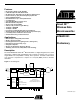
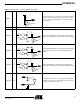
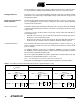
AT86RF401 Figure 3. Sample Circuit EXTERNAL LOOP FILTER (OPTIONAL) V+ R1 C2 C5 C4 C3 L1 U1 1 2 3 4 5 6 7 8 9 10 S1 ANT CFIL AVDD DVDD AGND DGND IO5 IO4 IO3 XTALB ANTB LOOPFIL L1 L2 RESETB NC IO0/SDI IO1/SDO IO2/SCLK XTAL/CLK V+ 20 19 18 17 16 15 14 13 12 11 C1 B1 S3 S2 Y1 RESET SDI SDO SCLK SPI Programming Interface Table 1. Recommended Parts List Part Number Value (Common) Value (315 MHz) Value (433.92 MHz) Value (Ext. Loop Filter) B1 3.6V CR2032, Li Battery C1 0.
Table 2. Pin Descriptions – 20-lead TSSOP Symbol Pin Description 1 ANTB 20 1 Differential Antenna Output 10 mA 2 VVCO VDD LOOPFIL VDD External VCO Loop-filter Connection. VVCO is the VCO control voltage. 2 3 4 2 VVCO VDD L1 VDD External VCO Inductor Connection. VVCO is the VCO control voltage. 3 3 4 2 VVDD VDD L2 External VCO Inductor Connection. VVCO is the VCO control voltage.
AT86RF401 Table 2. Pin Descriptions – 20-lead TSSOP (Continued) VDD SPI Reset Input: A “low” on this pin resets the device and puts the part into SPI mode. A logic-high on this pin causes the device to execute its program if the VDD is above the brownout voltage level. 35 k Ω RESETB 5 5 To AVR NC 6 No Connect. Float Pin. VDD I/O0 (SDI) 7 VDD Data Enable− 35 k Ω 7 SPI Data In/Input/Output 0: General-purpose I/O and button input. In SPI mode, this pin serves as SDI (Serial Data Input).
Table 2.
AT86RF401 Table 2. Pin Descriptions – 20-lead TSSOP (Continued) AVDD 18 Analog Voltage Supply 19 CFIL 19 External Data Rate Filter 1.
Absolute Maximum Ratings* Antenna Voltage (Pins 1, 20) ...................................... −1V to 10V *NOTICE: Operating Temperature........................................−40°C to +85°C Storage Temperature (without bias) ................−55°C to +125°C Voltage on VDD with respect to ground ............................. 6.0V Voltage on Pins 2–19 (TSSOP 20) ................ −0.1 to VDD +0.3V Stresses beyond those listed under “Absolute Maximum Ratings” may cause permanent damage to the device.
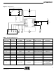
AT86RF401 Analog/RF Specs VDD = 3.3V; fXTAL = 13.125 MHz; fAVR = fXTAL ÷ 16; TA = 25°C unless otherwise specified. Symbol Parameter Conditions Min Typ Max Unit IPA Power Amp Output Current Transmitting (RF “ON”), 0 dB Attenuation – 8.
period. A number of registers are available to adjust the performance of the lock detector. These include lock delay and unlock delay timers as well as a cycle slip counter. Bandgap Reference The device uses a 1.2V (nominal) bandgap reference generator to provide consistent performance over a wide range of input supply voltages. This reference voltage is used throughout the device.
AT86RF401 Bit Timer A hardware assist has been included in the AT86RF401 to make transmission of data easier. Keying of the transmitter is timed by this logic, and interrupts are generated when data is needed by the timer or when transmission is complete. The timer also supports code that uses polling instead of interrupts. Using polling instead of interrupts may facilitate higher bit rates. Additionally, this timer may be used to time pulses arriving at the I/O3 pin.
Watchdog Timer When enabling the watchdog timer, the status of the watchdog time is unknown. The user is advised to execute a WDR instruction before enabling the watchdog. Otherwise, the device might get reset before the first WDR after enabling is reached. To prevent the unintentional disabling of the watchdog, a special turn-off procedure must be followed when the watchdog is disabled. Refer to the description of the Watchdog Timer Control Register on page 38 for details (see Register $22 in I/O Memory).
AT86RF401 During power-on reset and watchdog reset, all I/O registers are set to their initial values, and the program starts execution from address $000. Note: Interrupt Response Time The instruction placed in address $000 must be an RJMP (relative jump) instruction or a JMP (absolute jump) to the reset handling routine. If an RJMP or JMP instruction is not present at address $000, the part is placed into a “no program” reset state.
Serial Programming Algorithm Refer to Figure 4 (page 15), Figure 5 (page 16) and Figure 6 (page 17). To program and verify the AT86RF401 in the serial programming mode, the following sequence is recommended. Power-up Sequence: 1. Apply power between VDD and GND while RESETB and SCK are set to “0”. If a crystal is not connected across pins XTAL and XTALB, apply a clock signal to the XTAL pin.
AT86RF401 Data EEPROM Access from the AVR Table 6. AT86RF401 Serial Programming Instruction Set Instruction Format Instruction Byte 1 Byte 2 Byte 3 Byte 4 Operation Programming Enable 1010 1100 0101 0011 xxxx xxxx xxxx xxxx Enable Serial Programming after RESETB goes low.
Figure 5. Serial Programming Waveforms SERIAL DATA INPUT (SDI) SERIAL DATA OUTPUT (SDO) MSB LSB MSB LSB SERIAL CLOCK INPUT (SCK) Note: This device includes an integrated 128-byte EEPROM, which is accessed by three registers located in the I/O memory space. These are the DEECR, DEEDR and DEEAR registers. For more information, refer to I/O Register Description.
AT86RF401 Figure 6.
A flexible interrupt module has its control registers in the I/O space with an additional global interrupt enable bit in the status register. All interrupts have a separate interrupt vector in the interrupt vector table at the beginning of the program memory. The interrupts have priority in accordance with their interrupt vector position; the lower the interrupt vector address, the higher the priority. Figure 7.
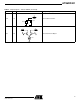
AT86RF401 General-purpose Register File Figure 8 shows the structure of the 32 general-purpose working registers in the CPU. Figure 8. AVR CPU General-purpose Working Registers 7 0 Addr.
The X, Y and Z Registers The registers R26...R31 have some added functions to their general-purpose usage. These registers are address pointers for indirect addressing of the data space. The three indirect address registers X, Y and Z are defined as shown in Figure 9. Figure 9.
AT86RF401 SRAM Data Memory Figure 10 shows how the AT86RF401 SRAM memory is organized. Figure 10. SRAM Organization Register File Data Address Space R0 R1 R2 ... $0000 $0001 $0002 ... R29 R30 R31 I/O Registers $00 $01 $02 ... $001D $001E $001F $3D $3E $3F $005D $005E $005F Internal SRAM $0060 $0061 ... $0020 $0021 $0022 ... $00DE $00DF The lower 224 Data Memory locations address the Register File, the I/O Memory and the internal data SRAM.
Register Direct, Single Register Rd Figure 11. Direct Single Register Addressing The operand is contained in register d (Rd). Register Direct, Two Registers Rd and Rr Figure 12. Direct Register Addressing, Two Registers Operands are contained in register r (Rr) and d (Rd). The result is stored in register d (Rd). I/O Direct Figure 13. I/O Direct Addressing Operand address is contained in 6 bits of the instruction word. “n” is the destination or source register address.
AT86RF401 Data Direct Figure 14. Direct Data Addressing Data Space 20 19 31 OP $00 16 Rr/Rd 16 LSBs 15 0 $DF A 16-bit Data Address is contained in the 16 LSBs of a two-word instruction. Rd/Rr specify the destination or source register. Data Indirect with Displacement Figure 15.
Data Indirect with Pre-decrement Figure 17. Data Indirect Addressing with Pre-decrement Data Space $0000 15 0 X, Y OR Z - REGISTER -1 $DF The X, Y or Z register is decremented before the operation. Operand address is the decremented contents of the X, Y or Z register. Data Indirect with Post-increment Figure 18. Data Indirect Addressing with Post-increment Data Space $0000 15 0 X, Y OR Z - REGISTER 1 $DF The X, Y or Z register is incremented after the operation.
AT86RF401 Indirect Program Addressing, IJMP and ICALL Figure 20. Indirect Program Memory Addressing $3FF Program execution continues at address contained by the Z register (i.e., the PC is loaded with the contents of the Z register). Relative Program Addressing, RJMP and RCALL Figure 21. Relative Program Memory Addressing 1 $3FF Program execution continues at address PC + k + 1. The relative address k is from − 2048 to 2047.
EEPROM Data Memory The AT86RF401 contains 128 bytes of data EEPROM memory. It is organized as a separate data space in which single bytes can be read and written. The access between the EEPROM and the CPU is described in the Memory Programming section (page 13). Memory Access Times and Instruction Execution Timing This section describes the general access timing concepts for instruction execution and internal memory access.
AT86RF401 Figure 24. On-chip Data SRAM Access Cycles T1 T2 T3 T4 System Clock Ø Address Data Write Data Read Write Prev. Address Read Address All I/Os and peripherals are placed in the I/O space. The I/O locations are accessed by the IN and OUT instructions, transferring data between the 32 general-purpose working registers and the I/O space. I/O registers within the address range $00–$1F are directly bit-accessible using the SBI and CBI instructions.
I/O Memory The I/O space definition of the AT86RF401 is shown in Table 7 below. Table 7.
AT86RF401 I/O and Control Registers The AT86RF401 I/Os and peripherals are placed in the I/O space. The various I/O locations are accessed by the IN and OUT instructions transferring data between the 32 general-purpose working registers and the I/O space. I/O registers within the address range $00–$1F are directly bit-accessible using the SBI and CBI instructions. In these registers, the value of single bits can be checked by using the SBIS and SBIC instructions.
Transmit Control Register – TX_CNTL Bit 7 6 5 4 3 2 1 0 $12 – – TXE TXK – LOC – – Read/Write R/W R/W R/W R/W R/W R/W R/W R/W Initial Value 0 0 0 0 0 0 0 0 • Bit[7:6] Reserved. • Bit[5]: TXE, Transmitter Enable This bit turns on the transmitter. • Bit[4]: TXK, Transmitter Key This bit is ORed with the output from the bit timer. If the bit timer is used to key the transmitter, the TXK bit should be programmed to “0”.
AT86RF401 • Bits[5:3]: PCC, Power Control (coarse) Attenuates the output power in 6 dB steps. PCC[5:3] Output Attenuation 000 0 dB 001 6 dB 010 12 dB 011 18 dB 100 24 dB 101 30 dB 110 Invalid 111 Invalid • Bits[2:0]: PCF, Power Control (fine) Attenuates the output power in 1 dB steps.
and 4 (L1 and L2) of the device. The capacitor array is set by VCOTUNE[4:0] and is comprised of the following switched capacitance levels: 32 VCOTUNE[4:0] Capacitance (pF) 00000 0 00001 0.03 00010 0.06 00011 0.09 00100 0.12 00101 0.15 00110 0.18 00111 0.21 01000 0.24 01001 0.27 01010 0.30 01011 0.33 01100 0.36 01101 0.39 01110 0.42 01111 0.45 10000 0.48 10001 0.51 10010 0.54 10011 0.57 10100 0.60 10101 0.63 10110 0.66 10111 0.69 11000 0.72 11001 0.
AT86RF401 • Bits[7:6]: VCO Voltage Detector The VCO Voltage Detector circuit monitors the level of the VCO control voltage. This circuit, along with the VCO Switch Caps and the Lock Detect circuit, is intended for use with a software algorithm to tune the VCO such that the VCO control voltage is centered approximately at 1.1V. The Voltage Detector circuit consists of two comparators with fixed reference voltages of V1 (lower reference voltage) and V2 (upper reference voltage).
• Bit[5:3]: ULC[2:0] The unlock count (ULC) bits count a certain number of reference clocks, after which the unlock detect circuit looks for a number of cycle slips determined by CS[1:0] before making the loc detect signal go low. The ULC bits essentially control the blackout period of the unlock detect circuit. The unlock counter is reset by the KEY signal rising (if ENKO is asserted), or by the LOC rising edge, or by the UPOK signal being set high.
AT86RF401 EEPROM Control Register Descriptions Data EEPROM Control Register – DEECR Bit 7 6 5 4 3 2 1 0 $1C – – – – BSY EEU EEL EER R/W R/W R/W R/W R R/W R/W R/W 0 0 0 0 0 0 0 0 Read/Write Initial Value 0 • Bits[7:4] R eserved . These b its should be “0 ” when written; otherw ise, results will b e unpredictable. • Bit[3]: EEPROM Busy Bit Initially set to “0”. This bit will be set high during writes to the EEPROM.
Data EEPROM Data Register – DEEDR Bit 7 6 5 4 3 2 1 0 $1D ED7 ED6 ED5 ED4 ED3 ED2 ED1 ED0 Read/Write R/W R/W R/W R/W R/W R/W R/W R/W 0 0 0 0 0 0 0 0 Initial Value 0 • Bits[7:0] This register contains the byte to be written to EEPROM. If a read operation has been done, this register contains that last byte read from the data EEPROM.
AT86RF401 Bit Timer Register Descriptions Bit Timer Count Register – BTCNT Bit 7 6 5 4 3 2 1 0 $20 C7 C6 C5 C4 C3 C2 C1 C0 Read/Write R/W R/W R/W R/W R/W R/W R/W R/W Initial Value 0 0 0 0 0 0 0 0 • Bit [7:0] Lowest 8 bits of countval. When combined with bits [7:6] of the BTCR register, countval determines a counter value that sets the width of a mark or a space that is sent to the transmitter.
• Bit[2]: Flag2 In transmit mode, this flag indicates the Transmit Done condition that occurs when the buffer is empty and the counter has counted down to “0”. In receive mode, this flag indicates that an edge has occurred, and the AVR should process the count value in the BTCR and BTCNT registers. This bit is cleared upon read, e.g., IN R16, BTCR. Mode[1:0] Flag2 Function 00 Disabled 01 Indicates Transmit Done condition; buffer is empty and the counter has expired.
AT86RF401 bit is set (“1”). To disable an enabled Watchdog Timer, the following procedure must be followed: In the same operation, write a logical “1” to WDTOE and WDE. A logical “1” must be written to WDE even though it is set to “1” before the disable operation starts. Within the next four clock cycles, write a logical “0” to WDE. This disables the watchdog.
• Bits[5:0] If set to “1”, the corresponding bit (pin) IO[5:0] is configured as an output. Data may then be written to that output by writing to the IO_DATA register. If set to “0”, the corresponding bit (pin) may be either a button input (refer to the Button Detect Register, $34) used to wake the part up or a normal digital input.
AT86RF401 • Bits[6:5]: AVR System Clock Select These bits select the divide value of the XTALB input that is used to produce the AVR System Clock. ACS[1:0] AVR System Clock 11 XTALB/16 10 XTALB/32 01 XTALB/64 00 XTALB/128 This clock select value may be programmed on the fly by either the AVR processor in normal operation or by an I/O write SPI command during SPI mode. Note that during SPI mode, the I/O and serial programming logic runs at XTALB/16 frequency.
Button Detect Register – B_DET Bit 7 6 5 4 3 2 1 0 $34 – – BD5 BD4 BD3 BD2 BD1 BD0 Read/Write R R R/W R/W R/W R/W R/W R/W Initial Value 0 0 0 0 0 0 0 0 • Bits[7:6] Reserved. These bits read “0”. • Bits[5:0] When an I/O pin is configured as a button using the IO_ENAB and IO_DATOUT registers and a logic low is detected on that pin, the button detect logic is activated. If the part is in sleep mode, the part responds as described in the Power Control Register description.
AT86RF401 The Stack Pointer – SP The Stack Pointer is implemented as two 8-bit registers in the I/O space locations $3E ($5E) and $3D ($5D). Caution: As the data memory has 224 locations, only 8 bits are used and the SPH register must be programmed to 0 x 00.
• Bit[4] – S: Sign Bit, S = N⊕V The S-bit is always an exclusive or between the negative flag N and the two’s complement overflow flag V. See Table 10 for detailed information. • Bit[3] – V: Two’s Complement Overflow Flag The two’s complement overflow flag V supports two’s complement arithmetics. See Table 10 below for detailed information. • Bit[2] – N: Negative Flag The negative flag N indicates a negative result after the different arithmetic and logic operations.
AT86RF401 Table 10.
Table 10.
AT86RF401 Table 10.
Ordering Information RF Output Ordering Code Package Application Temperature Operating Range 315 MHz AT86RF401U 20T North American −40°C to 85°C 434 MHz AT86RF401E 20T European −40°C to 85°C 264 to 456 MHz AT86RF401X 20T All Applications −40°C to 85°C 48 AT86RF401 1424D–RKE–09/02
AT86RF401 Package Drawing All devices are packaged on tape in reel; standard reel quantity is 2,500 pieces. 20A2 – TSSO b L L1 E E1 End View e COMMON DIMENSIONS (Unit of Measure = mm) Top View SYMBOL D D A A2 MIN NOM MAX NOTE 6.40 6.50 6.60 2, 5 4.40 4.50 3, 5 E E1 6.40 BSC 4.30 A – – 1.20 A2 0.80 1.00 1.05 b 0.19 – 0.30 e Side View L L1 Notes: 4 0.65 BSC 0.45 0.60 0.75 1.00 REF 1. This drawing is for general information only.
Atmel Headquarters Atmel Operations Corporate Headquarters Memory 2325 Orchard Parkway San Jose, CA 95131 TEL 1(408) 441-0311 FAX 1(408) 487-2600 Europe Atmel Sarl Route des Arsenaux 41 Case Postale 80 CH-1705 Fribourg Switzerland TEL (41) 26-426-5555 FAX (41) 26-426-5500 Asia Room 1219 Chinachem Golden Plaza 77 Mody Road Tsimhatsui East Kowloon Hong Kong TEL (852) 2721-9778 FAX (852) 2722-1369 Japan 9F, Tonetsu Shinkawa Bldg.