
Manual


26
AT86RF401
1424D–RKE–09/02
EEPROM Data Memory The AT86RF401 contains 128 bytes of data EEPROM memory. It is organized as a sep-
arate data space in which single bytes can be read and written. The access between the
EEPROM and the CPU is described in the Memory Programming section (page 13).
Memory Access Times
and Instruction
Execution Timing
This section describes the general access timing concepts for instruction execution and
internal memory access.
The AVR CPU is driven by the System Clock Ø generated from the main oscillator for
the chip. A programmable clock divider generates this clock from the crystal oscillator
input.
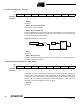
Figure 22 shows the parallel instruction fetches and instruction executions enabled by
the Harvard architecture and the fast-access register file concept. This is the basic pipe-
lining concept to obtain up to 1 MIPS per MHz with the corresponding unique results for
functions per cost, functions per clocks and functions per power unit.
Figure 22. The Parallel Instruction Fetches and Instruction Executions
Figure 23 shows the internal timing concept for the register file. In a single clock cycle,
an ALU operation using two register operands is executed, and the result is stored back
to the destination register.
Figure 23. Single Cycle ALU Operation
The internal data SRAM access is performed in two System Clock cycles as described
in Figure 24.
System Clock Ø
1st Instruction Fetch
1st Instruction Execute
2nd Instruction Fetch
2nd Instruction Execute
3rd Instruction Fetch
3rd Instruction Execute
4th Instruction Fetch
T1 T2 T3 T4
System Clock Ø
Total Execution Time
Register Operands Fetch
ALU Operation Execute
Result Write Back
T1 T2 T3 T4