
Manual


9
AT86RF401
1424D–RKE–09/02
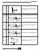
Note: 1. Characterized but not guaranteed by test due to dependency on PCB trace antenna
Functional
Description
The complete circuit consists of the following functional blocks.
Transmitter
Crystal Oscillator The crystal oscillator circuit is designed to work with crystals with fundamental frequen-
cies between 11 and 19 MHz. Forty pF of internal capacitance is connected between
each of the crystal input pins and (chip) ground. Alternatively, an external clock can be
used for these functions.
This circuit provides the master clock for the entire chip. A programmable divider is used
to provide the AVR system clock.
Radio Frequency Power
Amplifier
The RF power amplifier generates a differential output suitable for driving an off-chip
tuned-loop antenna from the PLL output. The PLL output signal is gated using on-off
keyed (OOK) modulation before transmission. It is used as the RF carrier frequency for
the transmitted data stream. The amplifier can be configured via software to reduce the
power output by 36 dB (with 1 dB resolution).
Frequency Synthesizer The frequency synthesizer utilizes a PLL, which consists of a phase detector, a ÷24
prescaler, an on-chip loop filter and an integrated VCO. The VCO output is buffered
prior to the output amplifier. The output frequency is 24 times the crystal frequency. To
offset component tolerance, a switched capacitor array is connected between pins 3
and 4 of the VCO. Thirty-two discrete steps of capacitance are available to tune the
VCO control voltage. An internal window comparator monitors the magnitude of the tun-
ing voltage and is used by the AVR core to determine the optimal tuning configuration.
Lock Detector The lock detection block provides an indication of the state of the phase lock loop (PLL).
Lock condition is determined by counting the number of cycle slips in a given time
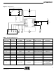
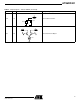
Analog/RF Specs
V
DD
=3.3V;f
XTAL
= 13.125 MHz; f
AVR
=f
XTAL
÷ 16; T
A
=25°C unless otherwise specified.
Symbol Parameter Conditions Min Typ Max Unit
RF Amplifier
I
PA
Power Amp Output Current Transmitting (RF “ON”), 0 dB Attenuation – 8.6 – mA
P
CTLRANGE
Power Control Range – 36 – dB
P
CTLRES
Power Control Resolution – 1 – dB
Crystal Oscillator
f
OSC
Oscillation Frequency Range 11 – 19 MHz
Frequency Synthesizer/PLL
F
OUT
Output Frequency Range 264 – 456 MHz
P
HARM
1
Harmonics
I/O Pins Static during RF Transmission
Using PCB Trace Antenna
– −60 – dBc
f
MOD
OOK Modulation Data Rate Using Manchester Data Bit Encoding ––10 Kbps