Features • Secure battery authentication • Superior SHA-256 Hash Algorithm • Best in class 256 bit key length • Guaranteed Unique 48 bit Serial Number • High speed single wire interface • Supply Voltage: 2.5 – 5.
1.1. 1.2. Memory Resources Sram 256 bits of SRAM that are used for storage of a key. The LoadSram command provides a mechanism to securely initialize this block during personalization. This memory will retain its value when the chip is put/goes to sleep, so long as a supply voltage in excess of VRETAIN is still supplied to the chip. MemValid A single bit that tells whether or not Sram contains valid data. It’s cleared when power is lost and set when the SRAM is loaded with a secret key.
AT88SA100S [ Preliminary] Status Fuses These fuses can be used to store various information which is not secret. Their value can always be determined using the Read command. They can be individually burned using the BurnFuse command. Two common usage models for these fuses are: 1. 2. 1.3. Consumption logging, i.e. burn one bit after every n uses, the host system keeps track of the number of uses so far for this serial number since the last fuse burn. Model number information.
1.4. Security Features This chip incorporates a number of physical security features designed to protect the key from unauthorized release. These include an active shield over the entire surface of the internal memory encryption, internal clock generation, glitch protection, voltage tamper detection and other physical design features. Both the clock and logic supply voltage are internally generated, preventing any direct attack via the pins on these two signals. 2.
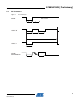
AT88SA100S [ Preliminary] 2.2. AC Parameters Figure 1.
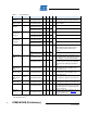
Table 3. AC Parameters Parameter Symbol Wake Low t WLO Duration Wake Delay to t WHI Data Comm. Start pulse t START duration Direction Min Typ Max Unit Notes To 60 μs Signal can be stable in either high or low CryptoAuthentication levels during extended sleep intervals. To 1 ms Signal should be stable high for this CryptoAuthentication entire duration. To 4.1 4.34 4.56 μs CryptoAuthentication From 4.62 6.0 8.
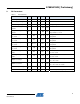
AT88SA100S [ Preliminary] 3. DC Parameters Table 4. DC Parameters Parameter Symbol Min Max Unit Operating temperature TA -40 85 °C Power Supply Voltage Vcc 2.5 5.5 V Fuse Burning Voltage VBURN 3.8 5.5 V Active Power Supply Current ICC 10 mA Sleep Power Supply Current I SLEEP 100 nA When chip is in sleep mode, Vsig = 0.0V, Vcc = 3.7V. Input Low Voltage @ Vcc = 5.5V VIL -0.5 .25 * Vcc V Voltage levels for wake token when chip is in sleep mode Input Low Voltage @ Vcc = 2.
3.1. IO Flags The host system is always the bus master, so before any IO transaction, the system must first send an 8 bit flag to the chip to indicate the IO operation that is to be performed, as follows: Value Name Meaning 0x77 Command After this flag, the system starts sending a command block to the chip. The first bit of the block can follow immediately after the last bit of the flag.
AT88SA100S [ Preliminary] 3.1.2. Transmit Flag The transmit flag is used to turn around the signal so that the device can send data back to the system, depending on its current state. The bytes that the device returns to the system, depending on its current state as follows: Table 6. Return Codes State Description After wake, but prior to first command After successful command execution Error/Status Description 0x11 Indication that a proper wake token has been received by the device.
3.2. IO Blocks Commands are sent to the chip, and responses received from the chip, within a block that is constructed in the following way: 3.3. Byte Number Name Meaning 0 Count Number of bytes to be transferred to the chip in the block, including count, packet and checksum, so this byte should always have a value of (N+1). The maximum size block is 39 and the minimum size block is 4. Values outside this range will cause unpredictable operation.
AT88SA100S [ Preliminary] 3.4.1. IO Timeout After a leading transition for any data token has been received, the device will expect another token to be transmitted within a tTIMEOUT interval. If the leading edge of the next token is not received within this period of time, the device assumes that the synchronization with the host is lost and transitions to a sleep state. After the device receives the last bit of a command block, this timeout circuitry is disabled.
4. Commands The command packet is broken down in the following way: Byte Name Meaning 0 Opcode The Command code 1 Param1 The first parameter – always present 2-3 Param2 The second parameter – always present 4+ Data Optional remaining input data If a command fails because the CRC within the block is incorrect, the opcode is invalid or one of the parameters is illegal, then immediately after tPARSE the system will be able to retrieve an error response block containing a single byte packet.
AT88SA100S [ Preliminary] 4.1. MAC Computes a SHA-256 digest of the key, challenge and other fixed information on the chip to generate an output response. If MemValid is not set, indicating that no valid key is stored in the SRAM, then this command will return an error.
4.2. Read Reads 4 bytes from Fuse, ROM or MemValid. Any attempt to present the chip with an illegal Fuse address will result in an error return. Table 10. Input Parameters Name Notes Opcode READ 1 0x02 Param1 Mode 1 Fuse, ROM or MemValid. Refer to 1.1. Param2 Address 2 Which 4 bytes within array. Bits 2-15 are ignored by the chip and should be 0’s. Data – 0 Table 11. Name Output Parameters Size Contents Table 12. Name 14 Size 4 Notes The contents of the specified memory location.
AT88SA100S [ Preliminary] 4.3. BurnFuse Burns one of the 88 user accessible fuse bits. The power supply pin must meet the VBLOW specification in order to burn fuses reliably. If the voltage is too low then the actual fuse blow will not be attempted and the chip will return the error code. If the watchdog timer is within tEXEC_FUSE of its expiration, this command will also be aborted and return an error.
4.4. GenPersonalizationKey This command generates a decryption digest that will be used by the subsequent command (LoadSram) to decrypt the key value that is to be written into the SRAM. This command must be run immediately prior to LoadSram within the same watchdog cycle. This command loads a transport key from an internal secure storage location and then uses that key along with an input seed to generate a decryption digest using SHA-256.
AT88SA100S [ Preliminary] 4.5. LoadSram Writes 256 bits into the battery backed SRAM and locks this memory against further modification. The value in the battery backed SRAM cannot be read, it must be verified via the MAC command. If the SRAM is already valid then this command will fail with an error response. The only way to unlock the SRAM is to remove power from the device.
4.6. PauseLong Forces the chip into a busy mode until the watchdog timer expires, after which it will automatically enter the sleep state. During execution of this command the chip will ignore all activity on the IO signal. This command is used to prevent bus conflicts in a system that also includes a CryptoAuthentication host chip sharing the same signal wire. Table 19.
AT88SA100S [ Preliminary] 6. Package Drawing 3TS1 - Shrink SOT 3 E1 CL L1 E 1 2 e1 End View Top View b A2 SEATING PLANE e A A1 D Side View Notes: 1. Dimension D does not include mold flash, protrusions or gate burrs. Mold flash, protrusions or gate burrs shall not exceed 0.25 mm per end. Dimension E1 does not include interlead flash or protrusion. Interlead flash or protrusion shall not exceed 0.25 mm per side. 2. The package top may be smaller than the package bottom.
7. Revision History Table 21. 20 Revision History Doc. Rev.
Headquarters International Atmel Corporation 2325 Orchard Parkway San Jose, CA 95131 USA Tel: 1(408) 441-0311 Fax: 1(408) 487-2600 Atmel Asia Room 1219 Chinachem Golden Plaza 77 Mody Road Tsimshatsui East Kowloon Hong Kong Tel: (852) 2721-9778 Fax: (852) 2722-1369 Atmel Europe Le Krebs 8, Rue Jean-Pierre Timbaud BP 309 78054 Saint-Quentin-enYvelines Cedex France Tel: (33) 1-30-60-70-00 Fax: (33) 1-30-60-71-11 Atmel Japan 9F, Tonetsu Shinkawa Bldg.