Features • Clock Controller • • • • • • • • • • • • – 80C51 core with 6 clocks per instruction – 8 MHz On-Chip Oscillator – PLL for generating clock to supply CPU core, USB and Smart Card Interfaces – Programmable CPU clock from 500 KHz / X1 to 48 MHz / X1 Reset Controller – Power On Reset (POR) feature avoiding an external reset capacitor – Power Fail Detector (PFD) – Watch-Dog Timer Power Management – Two power saving modes : Idle and Power Down – Four Power Down Wake-up Sources : Smart Card Detect
Reference Documents 2 The user must get the following additionnal documents which are not included but which complete this product datasheet • Product Errata Sheet • Bootloader Datasheet AT8xC5122/23 4202E–SCR–06/06
AT8xC5122/23 Product Description AT8xC5122/23 products are high-performance CMOS derivatives of the 80C51 8-bit microcontrollers designed for USB smart card reader applications. The AT8xC5122 is proposed in four versions : - ROM version with or without internal data E2PROM. The ROM device is only factory programmable. - CRAM version without internal data E2PROM.
Table 1.
AT8xC5122/23 8 MHz Oscillator RST 256 x 8 RAM 512 x 8 XRAM UART Interf ace PLL WATCH-DOG POR PFD RESET CVSS LI Alternate Card CVCC CIO1 CRST1 Interrupt Controller CCLK1 16-BIT TIMERS DC/DC Conv erter CPRES CRST ISO 7816 Interface PLLF 256 x 8 RAM 80C518-BIT CORE XTAL2 INT[0-1] XTAL1 T[0-1] RxD 3.
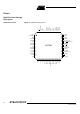
Pinout High Pin Count Package Description AVSS P2.3/A11 P2.4/A12 P2.5/A13 P2.6/A14 AVCC PLLF P2.2/A10 P2.0/A8 P2.1/A9 D+ D- P1.7/CCLK1 VREF Figure 1. VQFP64 Package Pinout CIO EA AT8xC5122 version 64 63 62 61 60 59 58 57 56 55 54 53 52 51 50 49 DVCC P1.2/CPRES 1 2 CC8 3 P5.7/KB7 P5.6/KB6 48 47 46 P3.1/TxD P1.6/SS P2.7/A15 4 5 45 P3.0/RxD 44 P3.5/T1/CRST1 CRST 6 P5.5/KB5 7 43 42 P3.2/INT0/LED0/CIO1 P4.0/MISO P5.4/KB4 8 41 P3.3/INT1 40 39 38 37 P4.1/MOSI P3.
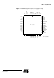
AT8xC5122/23 9 8 7 6 DVCC P1.2/CPRES CC8 P5.7/KB7 P5.6/KB6 P2.5/A13 P2.6/A14 N/A P2.3/A11 P2.4/A12 PLLF AVSS P2.2/A10 AVCC P2.1/A9 P2.0/A8 D+ D- EA P1.7/CCLK1 VREF CIO Figure 2. PLCC68 Package Pinout (for engineering purpose only) 5 4 3 2 1 68 67 66 65 64 63 62 61 60 59 58 10 11 12 13 N/A P3.1/TxD 57 P1.6/SS P2.7/A15 14 56 P3.0/RxD CRST P5.5/KB5 15 16 55 P5.4/KB4 17 18 P3.5/T1/CRST1 P3.2/INT0/LED0/CIO1 P4.0/MISO CC4 P5.3/KB3 P5.2/KB2 CCLK P5.1/KB1 P5.
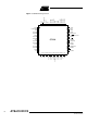
AVSS P2.3/A11 P2.4/A12 P2.5/A13 P2.6/A14 P2.2/A10 AVCC PLLF P2.0/A8 P2.1/A9 D+ D- P1.7/CCLK1 VREF CIO EA Figure 3. QFN64 Package Pinout 64 63 62 61 60 59 58 57 56 55 54 53 52 51 50 49 DVCC P1.2/CPRES 1 2 CC8 3 P5.7/KB7 P5.6/KB6 48 47 46 P3.1/TxD P1.6/SS P2.7/A15 4 5 45 P3.0/RxD 44 P3.5/T1/CRST1 CRST 6 P5.5/KB5 7 43 42 P3.2/INT0/LED0/CIO1 P4.0/MISO P5.4/KB4 8 41 P3.3/INT1 40 39 38 37 P4.1/MOSI P3.4/T0/LED1 36 35 34 P3.6/WR/LED2 P4.4/LED5 CC4 P5.3/KB3 P5.2/KB2 CCLK P5.
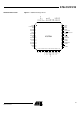
AT8xC5122/23 AVSS P2.3/A11 P2.4/A12 P2.5/A13 P2.6/A14 P2.2/A10 AVCC PLLF P2.0/A8 P2.1/A9 D+ D- P1.7/CCLK1 VREF Figure 4. VQFP64 Package Pinout CIO VCC AT89C5122DS version 64 63 62 61 60 59 58 57 56 55 54 53 52 51 50 49 DVCC P1.2/CPRES 1 2 CC8 3 P5.7/KB7 P5.6/KB6 48 47 46 P3.1/TxD P1.6/SS P2.7/A15 4 5 45 P3.0/RxD 44 P3.5/T1/CRST1 CRST 6 P5.5/KB5 7 43 42 P3.2/INT0/LED0/CIO1 P4.0/MISO P5.4/KB4 8 41 P3.3/INT1 40 39 38 37 P4.1/MOSI P3.4/T0/LED1 36 35 34 P3.6/WR/LED2 P4.
AVSS P2.3/A11 P2.4/A12 P2.5/A13 P2.6/A14 P2.2/A10 AVCC PLLF P2.0/A8 P2.1/A9 D+ D- P1.7/CCLK1 VREF CIO VCC Figure 5. QFN64 Package Pinout 64 63 62 61 60 59 58 57 56 55 54 53 52 51 50 49 DVCC P1.2/CPRES 1 2 CC8 3 P5.7/KB7 P5.6/KB6 48 47 46 P3.1/TxD P1.6/SS P2.7/A15 4 5 45 P3.0/RxD 44 P3.5/T1/CRST1 CRST 6 P5.5/KB5 7 43 42 P3.2/INT0/LED0/CIO1 P4.0/MISO P5.4/KB4 8 41 P3.3/INT1 40 39 38 37 P4.1/MOSI P3.4/T0/LED1 36 35 34 P3.6/WR/LED2 P4.4/LED5 CC4 P5.3/KB3 P5.2/KB2 CCLK P5.
AT8xC5122/23 Low Pin Count Package Description AVSS AVCC PLLF D+ D- Figure 6. PLCC28 Package Pinout CIO VREF AT8xC5122 and AT83C5123 versions 4 3 2 1 28 27 26 5 6 7 8 9 10 11 DVCC P1.2/CPRES CC8 CRST CC4 CCLK VSS 25 24 23 22 21 20 19 PLCC28 P3.1/TxD P3.0/RxD P3.2/INT0/LED0 P3.3/INT1 P3.4/T0/LED1 P3.6/LED2 RST XTAL1 XTAL2 VCC P3.7/LED3 AVSS PLLF DAVCC D+ VREF Figure 7. VQFP32 Package Pinout CIO P1.
AVSS PLLF DAVCC D+ VREF CIO P1.7/CCLK1 Figure 8. QFN32 Package Pinout 32 31 30 29 28 27 26 25 DVCC P1.2/CPRES CC8 CRST CC4 CCLK P5.0 VSS 1 2 3 4 5 6 7 8 24 23 22 21 20 19 18 17 QFN32 P3.1/TxD P1.6 P3.0/RxD P3.5/T1/CRST1 P3.2/INT0/LED0/CIO1 P3.3/INT1 P3.4/T0/LED1 P3.6/LED2 12 RST P3.
AT8xC5122/23 Pin Description QFN32 I/O Reset Level Alt Reset Config 30 - VCC 2KV I/O Float AD0 29 - VCC 2KV I/O Float - 28 - VCC 2KV I/O 38 - 27 - VCC 2KV - 36 - 25 - VCC 24 - 35 - 24 - P0.6 23 - 34 - 23 P0.7 22 - 33 - 22 PLCC28 ESD PLCC68 Supply Port VQFP32 Internal VQFP64 QFN64 Table 2. Pin Description P0.0 30 - 41 - P0.1 29 - 40 - P0.2 28 - 39 P0.3 27 - P0.4 25 P0.
QFN32 I/O Reset Level Alt Reset Config Conf 1 Conf 2 Conf 3 49 - VCC 2KV I/O 1 A14 Port51 Push-pull KB_OUT Input WPU 46 - VCC 2KV I/O 1 A15 Port51 Push-pull KB_OUT Input WPU 24 45 22 VCC 2KV I/O 1 RxD Port51 Push-pull KB_OUT Input WPU 59 25 48 24 VCC 2KV I/O 1 TxD Port51 Push-pull KB_OUT Input WPU 20 54 23 43 20 VCC 2KV I/O 1 INT0 Port51 41 19 52 22 41 19 VCC 2KV I/O 1 INT1 Port51 Push-pull KB_OUT Input WPU P3.
AT8xC5122/23 PLCC68 PLCC28 7 - 16 - P5.6 5 - 14 - P5.7 4 - 13 - QFN32 VQFP32 P5.5 QFN64 Port VQFP64 Table 2.
QFN32 QFN64 PLCC28 PLCC68 VQFP32 Port VQFP64 Table 2. Pin Description (Continued) Internal Power Supply ESD I/O Reset Level Alt Reset Config Conf 1 Conf 2 Conf 3 Led PSEN 15 - 24 - 15 - VCC O Program Strobe Enable: The read strobe to external program memory. When executing code from the external program memory, PSEN is activated twice each machine cycle, except that two PSEN activations are skipped during each access to external data memory.
AT8xC5122/23 Typical Applications Recommended External components All the external components described in the figure and table below must be implemented as close as possible from the microcontroller package. Table 3. External Components Bill Of Materials Reference Description R1 USB Full Speed Pull-up R2 USB pad serial resistor R3 USB pad serial resistor Value Comments 1.
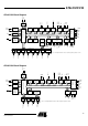
USB Keyboard with Smart Card Reader Using the AT8xC5122 and AT89C5122DS Versions VCC C9 C8 GND VCC GND VCC EA/VCC (1) 10mA Max VCC C1 GND VCC AVCC LEDx VCC DVCC L1 C4 LI GND USB R1 VCC VBUS D+ VREF CVCC D+ CVSS D- CRST CCLK CC4 CIO CC8 CPRES R2 Smart Card C7 C1 VCC C5 GND GND R3 DGND C6 GND R00 R01 R02 R03 R04 R05 R06 R07 R08 R09 R10 R11 R12 R13 R14 R15 R16 R17 R18 R19 C0 C1 C2 C3 C4 C5 C6 C7 C2 C3 C4 C7 C8 S1 S2 R5 KB0 KB1 KB2 KB3 KB4 KB5 KB6 KB7 GND VCC Keyboard Ma
AT8xC5122/23 USB Smart Card Reader Using the AT83C5123 Version VCC VCC C9 C8 GND VCC GND VCC EA 10mA Max C1 GND VCC AVCC LEDx VCC DVCC L1 C4 LI Smart Card GND USB CVCC R1 VCC C6 C7 C1 VCC VREF VBUS D+ D+ R3 DGND C5 GND CVSS R2 GND C2 C3 C4 C7 C8 S1 CRST CCLK CC4 CIO CC8 CPRES D- GND RST CLK C4 I/O C8 S1 S2 R5 GND VCC Alternate Card C1 C2 C3 C7 C5 CRST1 CCLK1 CIO1 VCC RST CLK I/O GND GND PLLF RST AVSS VSS R4 XTAL1 XTAL2 C2 C10 Optional Capacitor GND C3 GND G
Memory Organization The AT8xC5122/23 devices have separated address spaces for Program and Data Memory, as shown in Figure 13 on page 29, Figure 14 on page 31 and Figure 15 on page 32. The logical separation of Program and Data memory allows the Data Memory to be accessed by 8-bit addresses, which can be more quickly stored and manipulated by an-bit CPU. Nevertheless, 16-bit Data Memory addresses can also be generated through the DPTR register.
AT8xC5122/23 Data Memory Managament All device versions implements : - 256 Bytes of RAM to increase data parameter handling and high level language usage - 512 bytes of XRAM (Extended RAM) to store program data. RAM Achitecture The internal RAM is mapped into three separate segments : • The Lower 128 bytes (addresses 00h to 7Fh) are directly and indirectly addressable. • The Upper 128 bytes (addresses 80h to FFh) are indirectly addressable only.
An access to external XRAM memory locations higher than the accessible size of the memory (roll-over feature) will be performed with the MOVX DPTR instructions, with P0 and P2 as data/address busses, WR and RD as respectively write and read signals. Accesses above XRAM size can only be done by the use of DPTR. If EXTRAM=1 the MCU fetches the data from external XRAM Memory. There can be up to 64 KBytes of external XRAM Memory.
AT8xC5122/23 Figure 11. Use of Dual Pointer External Data Memory 7 0 DPS AUXR1(A2H) DPTR1 DPTR0 DPH(83H) DPL(82H) a. Bit 2 stuck at 0; this allows to use INC AUXR1 to toggle DPS without changing GF3.
Registers Table 5. Auxiliary Register - AUXR (8Eh) 7 6 5 4 DPU - - - Bit Number 3 2 1 0 XRS0 EXTRAM AO Bit Mnemonic Description Disable weak Pull-up 7 DPU 6-3 - 2 XRS0 0 weak pull-up is enabled 1 weak pull-up is disabled Reserved The value read from this bit is indeterminate. Do not change these bits. XRAM Size 0 256 bytes (default) 1 512 bytes EXTRAM bit Cleared to access internal XRAM using MOVX @ Ri/ @ DPTR. 1 EXTRAM Set to access external memory.
AT8xC5122/23 Table 6. Auxiliary Register 1 AUXR1- (0A2h) for AT8xC5122 7 6 5 4 3 2 1 0 - - ENBOOT - GF3 0 - DPS Bit Number 7-6 Bit Mnemonic Description Reserved The value read from this bit is indeterminate. Do not change these bits. - Enable Boot ROM (CRAM / E2PROM version only) 5 ENBOOT Set this bit to map the Boot ROM from 8000h to FFFFh. If the PC increments beyond 7FFFh address, the code is fetch from internal ROM Clear this bit to disable Boot ROM.
Table 8. CRAM Configuration Register - RCON (D1h) 7 6 5 4 3 2 1 0 - - - - RPS - - - Bit Bit Number Mnemonic 7-4 - Description Reserved The value read from this bit is indeterminate. Do not change these bits. CRAM Memory Mapping Bit 3 RPS Set to map the CRAM memory during MOVX instructions Clear to map the XRAM memory during MOVX. This bit has priority over the EXTRAM bit. 2-0 - Reserved The value read from this bit is indeterminate. Do not change these bits.
AT8xC5122/23 AT8xC5122 Microcontroller FFFFh P3.7 Bootloader 7FFFh 7F00h 7EFFh Reserved User code 0000h When pin EA =1 and after the reset, the MCU begins the execution of the embedded bootloader from location F800h of the ROM. The bootloader implements an In-System Programming (ISP) mode which manages the transfer of the code in the volatile Program Memory (CRAM).
Using CRAM Memory The CRAM is a read / write volatile memory that is mapped in the program memory space. Then when the power is switched off the code is lost and needs to be reload at each power up. In return, the CRAM enables a lot of flexibility in the code development as it can be programmed indefinitely. The user code running in the CRAM can perform read operations in CRAM itself by means of MOVC instructions like any C51 microcontroller does.
AT8xC5122/23 Figure 13.
AT8xC5122’s ROM Version The AT8xC5122’s ROM version implements : - 32 K of ROM mapped from 0000h to 7FFFh in which is embedded the user code. The ROM device is only factory programmable. - 512 bytes of E2PROM can be optionally implemented to store permanent data. With this option, the size of ROM is reduced to 30K. After the reset, the MCU begins the execution of the user code from location 0000h of the ROM. Access to external Program Memory is not allowed.
AT8xC5122/23 Figure 14.
AT83C5123 Version The AT83C5123 device is a low pin count version of the AT8xC5122. The ROM version implements : - 30 KB of ROM mapped from 0000 to 77FF in which is embedded the user code. The ROM device is only factory programmable. - 512 bytes of E2PROM can be optionally implemented to store permanent data Figure 15.
AT8xC5122/23 Special Function Registers (SFR’s) Introduction The Special Function Registers (SFRs) of the AT8xC5122/23 can be ranked into the following categories: • C51 Core Registers: ACC, B, DPH, DPL, PSW, SP • System Configuration Registers: PCON, CKRL, CKCON0, CKCON1, CKSEL, PLLCON, PLLDIV, AUXR, AUXR1, RCON • I/O Port Registers: P0, P1, P2, P3, P4, P5, PMOD1, PMOD2 • Timer Registers: TCON, TH0, TH1, TMOD, TL0, TL1 • Watchdog (WD) Registers: WDTRST, WDTPRG • Serial I/O Port Registers: SADDR
AT8xC5122 Version Bit addressable 0/8 F8h UEPINT 0000 0000 F0h B 0000 0000 E8h E0h Not bit addressable 1/9 2/A 3/B 4/C 5/D UEPCONX 1000 0000 UEPRST 0000 0000 6/E 7/F UEPSTAX 0000 0000 UEPDATX 0000 0000 LEDCON0 0000 0000 P5 1111 1111 LEDCON1 ACC 0000 0000 XX00 0000 PSW 0000 0000 XXXX 0XXX UBYCTX 0000 0000 D8h D0h RCON C8h S 1 C R S 0 C0h S 1 C R S 0 P4 1111 1111 0X10 1111 SCWT3 (1) B0h A8h A0h 98h 90h 88h 80h IPL0 SADEN X000 000 0000 0000 P3 1111 1111 IEN1 XXXX X0
AT8xC5122/23 AT83C5123 Version Bit addressable 0/8 F8h UEPINT 0000 0000 F0h B 0000 0000 E8h E0h Not bit addressable 1/9 2/A 3/B 4/C 5/D UEPCONX 1000 0000 UEPRST 0000 0000 6/E 7/F UEPSTAX 0000 0000 UEPDATX 0000 0000 USBADDR 1000 0000 UEPNUM 0000 0000 0000 0000 LEDCON0 0000 0000 P5 XXXX XXX1 ACC 0000 0000 UBYCTX 0000 0000 D8h D0h PSW 0000 0000 C8h S 1 C R S 0 SCICLK (1) C0h S 1 C R S 0 11XX XXXX 0X10 1111 SCWT3 (1) UEPIEN 0000 0000 0000 0000 B8h S 1 C R S 0 P4 B0h A8h IP
SFR’s Description Table 10. C51 Core SFRs Mnemonic Add Name 7 6 5 4 3 2 1 0 ACC E0h Accumulator B F0h B Register PSW D0h Program Status Word RS0 OV F1 P SP 81h Stack Pointer DPL 82h Data Pointer Low byte (LSB of DPTR) DPL DPH 83h Data Pointer High byte (MSB of DPTR) DPH 4 3 2 1 0 GF1 GF0 PD IDL T1X2 T0X2 X2 ACC B CY AC F0 RS1 SP Table 11.
AT8xC5122/23 Table 13. Timers SFRs Mnemonic Add Name 7 6 5 4 3 2 1 0 TH0 8Ch Timer/Counter 0 High byte TH0 TL0 8Ah Timer/Counter 0 Low byte TL0 TH1 8Dh Timer/Counter 1 High byte TH1 TL1 8Bh Timer/Counter 1 Low byte TL1 TCON 88h Timer/Counter 0 and 1 control TF1 TR1 TF0 TR0 IE1 IT1 IE0 IT0 TMOD 89h Timer/Counter 0 and 1 Modes GATE1 C/T1# M11 M01 GATE0 C/T0# M10 M00 7 6 5 4 3 2 1 0 Table 14.
Table 17. Interrupt SFRs Mnemonic Add Name 7 IPH0 B7h Interrupt Priority Control High 0 IPL1 B2h Interrupt Priority Control Low 1 IPH1 B3h Interrupt Priority Control High 1 ISEL A1h Interrupt Enable Register Note: 6 4 3 2 1 0 PSH PT1H PX1H PT0H PX0H PUSBL PSCIL PSPIL(1) PKBL (1) PUSBH PSCIH PSPIH(1) PKBH(1) RXIT OELEV OEEN PRESEN RXEN 4 3 2 1 0 CPLEV 5 PRESIT 1. Only for AT8xC5122 Table 18.
AT8xC5122/23 Table 18. SCIB SFRs Mnemonic Add Name SCICLK C1h 7 Smart Card Frequency Prescaler Register Note: 6 5 4 3 XTSCS(1) 2 1 0 1 0 SCICLK5-0 1. Only for AT8xC5122 Table 19. DC/DC SFRs Mnemonic Add Name DCCKPS BFh DC/DC Converter Reload Register 7 6 MODE OVFADJ 7 6 5 4 3 2 BOOST[1-0] DCCKPS3-0 Table 20.
Table 22. USB SFRs Mnemonic Add Name 7 UEPIEN C2h UEPDATX CFh USB Endpoint X Fifo Data UBYCTX E2h UFNUML BAh USB Frame Number Low UFNUMH BBh USB Frame Number High USB Endpoint Interrupt Enable 6 5 4 3 2 1 0 EP6INTE EP5INTE EP4INTE EP3INTE EP2INTE EP1INTE EP0INTE FDAT7 - 0 USB Byte Counter Low BYCT6-0 (EPX) FNUM7 - 0 CRCOK CRCERR 5 4 FNUM10-8 Table 23.
AT8xC5122/23 Clock Controller The clock controller is based on an on-chip oscillator feeding an on-chip Phase Lock Loop (PLL). All the internal clocks to the CPU core and peripherals are generated by this controller. On-Chip Oscillator The on-chip oscillator is composed of a single-stage inverter and a parallel feedback resistor. The XTAL1 and XTAL2 pins are respectively the input and the output of the inverter, which can be configured with off-chip components as a Pierce oscillator (see Figure 16).
Phase Lock Loop (PLL) PLL Description The AT8xC5122/23’s PLL is used to generate internal high frequency clock synchronized with an external low-frequency. Figure 17 shows the internal structure of the PLL. The PFLD block is the Phase Frequency Comparator and Lock Detector.
AT8xC5122/23 Figure 19. PLL Programming Flow PLL Programming Configure Dividers N3:0= xxxxb R3:0= xxxxb Enable PLL PLLEN= 1 PLL Locked? PLOCK= 1? Clock Tree Architecture The clock controller outputs several different clocks as shown in Figure 20: • a clock for the CPU core • a clock for the peripherals which is used to generate the timers, watchdog, SPI, UART, and ports sampling clocks. This divided clock will be used to generate the alternate card clock.
Figure 20. Clock Tree Diagram CK_DCDC PR4 DC/DC Converter DCCKPS[3:0] CKCON0.X or CKCON1.0 PeriphX2 CKCON0.0 Peripherals X2 1 1 CK_PERIPH 0 1/2 0 CK_T0 CK_T1 CK_SI CK_WD CK_SPI PERIPH = T0, T1, SI, WD or SPI CK_XTAL1 0 PR1 CK_PLL 1 0 CKRL[3:0] CPU 1 CKS CKSEL.0 X2 CKCON0.0 CK_XTAL1 PLL 96 MHz XTAL1 CK_CPU CK_IDLE IDL PCON.0 Alternate Card PR3 CK_PLL SCSR[3:2] XTAL2 PLLEN CK_IDLE CK_PLL PLLCON.1 0 CK_XTAL1 PR2 1 SCICLK[5:0] PD <48 CK_ISO SCIB =48 PCON.
AT8xC5122/23 The CPU and peripherals clocks frequencies are defined in the table below. X1 and X2 Modes CKS X2 FCK_IDLE 0 0 FCK_XTAL1/(2*(16-CKRL)) 0 1 FCK_XTAL1 1 0 FCK_PLL/(2*(16-CKRL)) 1 1 Not allowed Use of on-chip oscillator When the CPU and Peripherals clocks are fed by the on-chip oscillator, the CPU and Peripherals can be configured independently in X1 or X2 mode depending on the frequencies wanted by the user.
Figure 21. X1 mode Crystal PR1 prescaler 8 MHz 1/2 CPU frequency 4 MHz Peripheral frequency 4 MHz When the X1 mode is selected, the CPU and Peripherals work at 8Mhz / X1 Figure 22. X2 mode CPU frequency (X2 Mode) Crystal 8 MHz 8 MHz Peripheral frequency (X2 mode) 8 MHz Internal Prescaler 1/2 Peripheral frequency (X1 mode) 4 MHz When the X2 mode is selected, the CPU works at 8 MHz / X2. The Peripherals can work at 8 MHz / X2 or 8 MHz / X1.
AT8xC5122/23 Crystal 8 MHz PR1 Prescaler CPU frequency 1/8 1 MHz PERIPH frequency 1 MHz (Equivalent to) External Clock 2 MHz X1 mode selected CPU frequency 1 MHz 1/2 PERIPH frequency 1 MHz (Equivalent to) External Clock 1 MHz CPU frequency X2 mode selected 1 MHz PERIPH frequency 1 MHz Use of PLL Clock When the CPU clock is fed by the PLL, the X2 mode is forbidden. The bit X2 must always remain cleared in CKCON0 register.
PLL Prescaler CPU frequency 1/4 96 MHz 24 MHz PERIPH frequency 24 MHz (Equivalent to) External Clock X1 mode selected CPU frequency 1/2 48 MHz 24 MHz PERIPH frequency 24 MHz (Equivalent to) CPU frequency External Clock 24 MHz X2 mode selected 24 MHz PERIPH frequency 24 MHz SCIB Clock The Smart Card Interface Block (SCIB) uses two clocks : – The first one, CK_IDLE, is the peripheral clock used for the interface with the microcontroller.
AT8xC5122/23 If the CK_CPU <= 4/3 * CK_ISO, the SCIB doesn’t work. If the CK_CPU >= 6* CK_ISO, the programmer must take care in three cases: • Read (or write) operation on a SCIB register followed immediatly with an other Read (or write) operation on the same register. • Read (or write) operation on a SCIB register followed immediatly with an other Read (or write) operation on a linked register. The list of linked registers is in the table below.
USB Interface Clock The USB Interface uses two clocks : – The first one is the CPU clock used for the interface with the microcontroller, CK_IDLE. – The second one is the CK_USB supplied from the PLL through a divider by 2. Registers Table 24. Clock Selection Register - CKSEL (S:85h) 7 6 5 4 3 2 1 0 - - - - - - - CKS Bit Number Bit Mnemonic Description 7:1 - 0 CKS Reserved The value read from this bit is indeterminate. Do not set this bit.
AT8xC5122/23 Table 26. Clock Configuration Register 0 - CKCON0 (S:8Fh) 7 6 5 4 3 2 1 0 - WDX2 - SIX2 - T1X2 T0X2 X2 Bit Number Bit Mnemonic Description 7 - Reserved The value read from this bit is indeterminate. Do not set this bit. Watchdog clock 6 WDX2 This control bit is validated when the CPU clock X2 is set; when X2 is low, this bit has no effect. Cleared to bypass the PR1 prescaler. Set to select the PR1 output for this peripheral.
Table 27. Clock Configuration Register 1 - CKCON1 (S:AFh) only for AT8xC5122 7 6 5 4 3 2 1 0 - - - - - - - SPIX2 Bit Number Bit Mnemonic Description 7-4 - Reserved The value read from this bit is indeterminate. Do not set this bit. 3 - Reserved The value read from this bit is indeterminate. Do not set this bit. SPI clock 0 SPIX2 This control bit is validated when the CPU clock X2 is set. When X2 is low, this bit has no effect. Cleared to bypass the PR1 prescaler.
AT8xC5122/23 I/O Port Definition Ports vs Packages Port 0 Table 30. I/O Number vs Packages P0 P1 P2 P3 P4 P5 Total VQFP64 QFN64 8 8 8 8 6 8 46 VQFP32 QFN32 - 8 - 8 - 1 17 PLCC28 - 6 - 6 - 1 13 Port 0 has the following functions: – Default function: Port 0 is an 8-bit I/O port. – Alternate function: Port 0 is also the multiplexed low-order address and data bus during accesses to external Program and Data Memory.
Port 1 Port 1 has the following functions: – Default function : Only Port 1.2, P1.6 and P1.7 are standard I/O’s; the other ports can be activated only with the SCIB function. – Alternate function and configuration: see Table 31. Table 31. Port 1 Description. Port Alternate Function Configuration Signal Description Mode Smart card interface function Quasi-bidirectional port supplied by DC/DC converter CIO CC8 P1.2 CPRES CC4 CCLK CRST P1.
AT8xC5122/23 Port 3 Port 3 has the following functions: – Default function: Port 3 is an 8-bit I/O port. – Alternate functions: see table below Port 3 has the following configurations: – Default configuration: Pseudo bi-directional “Port51” digital input/output with internal pull-ups. – Alternate configurations: See Table 32. Table 32. Port 3 Description Alternate Functions Configurations Port Signal Description Mode 1 Mode 2 Mode 3 Mode 4 P3.
Port 4 Port 4 has the following functions: – Default function: Port 4 is an 6-bit I/O port. – Alternate functions: see table below Port 4 has the following configurations: – Default configuration: Pseudo bi-directional “Port51” digital input/output with internal pull-ups. – Alternate configurations: See Table 33. Table 33. Port 4 Description Alternate Functions Port 5 Configurations Port Signal Description Mode 1 Mode 2 Mode 3 P4.0 MISO SPI Master In Slave Out I/O P4.
AT8xC5122/23 Port Configuration Standard I/O P0 The P0 port is described in Figure 23. Figure 23. Standard Input/Output Port ADDR/DATA CONTROL Vcc PMOS 1 Port latch Data NMOS Pin 0 MUX Vss Input Data Quasi Bi-directional Port The default port output configuration for standard I/O ports is the quasi-bi-directional output that is common on the 80C51 and most of its derivatives. The “Port51” output type can be used as both an input and output without the need to reconfigure the port.
The “Port51” is described in Figure 24. Figure 24. Quasi Bi-directional Port DPU (AUXR.7) 2 CPU CLOCK DELAY vcc P Strong Port Latch Data vcc vcc P P Weak Medium Pin N Vss Input Data Push-pull Output Configuration The push-pull output configuration has the same pull-down structure as both the open drain and the quasi-bi-directional output modes, but provides a continuous strong pullup when the port latch contains a logic 1.
AT8xC5122/23 Figure 26. Input with Pull-up P Stuck to 0 if Medium Medium P Stuck to 0 if Weak Weak Input Data Pin Input with Weak Pull-down Configuration The input with pull-down (input WPD) configuration is shown in Figure 27 Figure 27. Input with Pull-down Input Data N 1 Low Speed Output Configuration Pin Weak The low speed output with low speed tFALL and tRISE can drive keyboard. The current limitation of the LED2CTRL block requires a polarisation current of about 250 µA.
Figure 29. LED Source Current Pin NMOS N LEDx.0 N Port Latch Data LEDx.1 Notes: LEDCTRL 1. When switching a low level, LEDCTRL device has a permanent current of about N mA/15 (N is 2, 4 or 8). 2. The port must be configured as standard C51 port by means of PMOD0 and PMOD1 registers and the level of current must be programmed by means of LEDCON0 and LEDCON1 registers before switching the led on. Table 35. LED Source Current LEDx.1 LEDx.
AT8xC5122/23 Registers Table 36. Port Mode Register 0 - PMOD0 (91h) for AT8xC5122 7 6 5 4 3 2 1 0 P3C1 P3C0 P2C1 P2C0 CPRESRES - P0C1 P0C0 Bit Number Bit Mnemonic Description Port 3 Configuration bits (Applicable to P3.0, P3.1, P3.3, P3.
Table 38. Port Mode Register 1 - PMOD1 (84h) for AT8xC5122 7 6 5 4 3 2 1 0 P5HC1 P5HC0 P5MC1 P5MC0 P5LC1 P5LC0 P4C1 P4C0 Bit Number Bit Mnemonic Description Port 5 High Configuration bits (Applicable from P5.6 to P5.7 only) 00 Quasi bi-directional 7-6 P5HC1-P5HC0 01 Push-pull 10 Input with weak pull-down 11 Input with weak pull-up Port 5 Medium Configuration bits (Applicable from P5.3 to P5.
AT8xC5122/23 Table 40. LED Port Control Register 0 - LEDCON0 (F1h) 7 6 5 4 3 2 1 0 LED3.1 LED3.0 LED2.1 LED2.0 LED1.1 LED1.0 LED0.1 LED0.0 Bit Number Bit Mnemonic Description Port LED3 Configuration bits 7-6 LED3 00 01 10 11 LED control disabled 2 mA current source when P3.7 is configured as Quasi-bi-directional mode 4 mA current source when P3.7 is configured as Quasi-bi-directional mode 10 mA current source when P3.7 is configured as Quasi-bidirect.
Smart Card Interface Block (SCIB) The SCIB provides all signals to interface directly with a smart card. The compliance with the ISO7816, EMV’2000, GSM and WHQL standards has been certified. Both synchronous (e.g. memory card) and asynchronous smart cards (e.g. microprocessor card) are supported. The component supplies the different voltages requested by the smart card. The power off sequence is directly managed by the SCIB.
AT8xC5122/23 Block Diagram The Smart Card Interface Block diagram is shown Figure 30: Figure 30. SCIB Block Diagram Barrel shifter IO (in) Clk_iso IO (out) Clk_cpu CLK I/O mux Etu counter Guard time counter Scart fsm Waiting time counter RST C4 (out) C8 (out) C4 (in) SCI Registers C8 (in) Power on INT Interrupt generator Power off VCARD fsm Definitions This paragraph introduces some of the terms used in ISO 7816-3 and EMV recommendations.
ATR Answer To Reset. Response from the ICC to a Reset initiated by the Terminal F and D F = Clock Rate Conversion Factor, D = Bit rate adjustment factor. ETU is defined as : ETU = F/(D*f) with f = Card Clock frequency. If f is in Hertz, ETU is in second. F and D are available in the ATR (byte TA1). The default values are F=372, D=1. Guard Time The time between 2 leading edges of the start bit of 2 consecutive characters is comprised of the character duration (10) plus the guard time.
AT8xC5122/23 IEC7816-3 says this procedure is mandatory in ATR for card supporting T=0 while EMV says this procedure is mandatory for T=0 but does not apply for ATR.
The Guard Time counter is an 9 bit counter It is initialized at 001h at the start of a transmission by the Terminal. It then increments itself at each ETU until it reach the 9 bit value loaded into the SCGT1[0] concatenated with SCGT0[7:0]. At this time a new Terminal transmission is enabled and the Guard Time Counter stop incrementing. As soon as a new transmission start, the Guard Time Counter is re-initialized at 1 decimal value. It should be noted that the value of the Guard Time Counter cannot be red.
AT8xC5122/23 Figure 32. Block Guard Time. TRANSMISSION to ICC RECEPTION from ICC Write SCGT1,0 with a value for Guard Time CHAR 1 CHAR 2 CHAR n CHAR n+1 CHAR n+2 CHAR n+3 >= SCGT >= Block Guard Time Write “Block Guard Time” in SCGT1,0 and set BGTEN to transfer the value to the shadow SCGT1,0 registers Figure 33.
When the WT counter times out, an interrupt is generated and the SCIB function is locked: reception and emission are disabled. It can be enabled by resetting the macro or reloading the counter. The Waiting Time Counter can be used in T=0 protocol for the Work Waiting Time. It can be used in T=1 protocol for the Character Waiting Time and for the Block Waiting Time. See the detailed explanation below. Figure 34.
AT8xC5122/23 Figure 35. T=0 mode > GT CHAR 2 CHAR 1 < WT In T=1 protocol : The maximum interval between the leading edge of the start bit of 2 consecutive characters sent by the ICC is called maximum Character Waiting Time. The Character Waiting Time shall not exceed (2**CWI + 11) ETUs with 0 =< BWI =< 5. Consequently 12 ETUs =< CWT =< 43 ETUs. T=1 protocol also specify the maximum Block Waiting Time.
Power-on and Power-off FSM The Power-on Power-off Finite State Machine (FSM) applies the signals on the smart card in accordance with ISO7816-3 standard. It conducts the Activation (Cold Reset and Warm Reset as well as De-Activation) it also manages the exception conditions such as overcurrent (see DC/DC Converter) To be able to power on the SCIB, the card presence is mandatory. Upon detectection of a card presence, the Terminal initiate a Cold Reset Activation.
AT8xC5122/23 Removal of the smart card will automatically start the power off sequence as described in Figure 39. The SCIB deactivation sequence after a reset of the CPU or after a lost of power supply is ISO7816-3 compliant. The switching order of the signals is the same as in Figure 39 but the delay between signals is analog and not clock dependant. Figure 39.
Additional Features Clock The CK_ISO input must be in the range 1 - 5 MHz according to ISO 7816. The CK_ISO can be programmed up to 12 MHz. In this case, the timing specification of the output buffer will not comply to ISO 7816. Figure 41. Clock Diagram of the SCIB Block CK_IDLE Ck_cpu CK_PLL or CK_XTAL1 Ck_ISO PR2 SCIB Figure 42. Prescaler 2 Description PR2 CK_PLL 0 CK_XTAL1 1 1/(2*(48 - SCICLK[5-0])) <48 CK_ISO =48 XTSCS SCICLK.7 SCICLK[5:0] EXT48 PLLCON.
AT8xC5122/23 Transmit / Receive Buffer The contents of the SCIBUF Transmit / Receive Buffer is transferred or received into / from the Shift Register. The Shift Register is not accessible by microcontroller. Its role is to prepare the byte to be copied on the I/O pin for a transmission or in the SCIBUF buffer after a reception.
Figure 43.
AT8xC5122/23 Figure 44. Character Reception Diagram SCISR register SCTC SCTBE Shift Register SCRC SCPE Parity error SCIBUF Received Character I/O pin SCIER Register ESCTBI SCTBI ESCTI ESCRI Parity error SCTI SCRI SCPI SCIIR register SCIB Reset The SCICR register contains a reset bit. If set, this bit generates a reset of the SCIB and its registers. Table 43 defines the SCIB registers that are reset and their reset values. Table 43.
Alternate Card A second card named ‘Alternate Card’ can be controlled. The Clock signal CCLK1 can be adapted to the XTAL frequency. Thanks to the clock prescaler which can divide the frequency by 1, 2, 4 or 8. The bits ALTKPS0 and ALTKPS1 in SCSR Register are used to set this factor. Figure 45. Alternate Card CVCC CRST CIO CCLK SMART CARD Main card CPRES 1, 1/2, 1/4 or 1/8 CK_IDLE PR3 P1.7 ALTKPS0,1 SCSR Reg. 1 0 CCLK1 SIM, SAM CARD Alternate card SCCLK1 SCSR Reg.
AT8xC5122/23 Table 44. Smart Card Interface Control Register - SCICR (S:B6h, SCRS = 1) 7 6 5 4 3 2 1 0 RESET CARDDET VCARD1 VCARD0 UART WTEN CREP CONV Bit Number 7 Bit Mnemonic RESET Description Reset Set this bit to reset and deactivate the Smart Card Interface. Clear this bit to activate the Smart Card Interface. This bit acts as an active high software reset.
Table 45. Smart Card Contacts Register - SCCON (S:ACh, SCRS=0) 7 6 5 4 3 2 1 0 CLK - CARDC8 CARDC4 CARDIO CARDCLK CARDRST CARDVCC Bit Number 7 Bit Mnemonic CLK Description Card Clock Selection Clear this bit to use the Card CLK bit (CARDCLK bit below) to drive Card CLK (P1.4) pin. Set this bit to use CK_XTAL1 or CK_PLL signals for CK_ISO to drive the Card CLK pin (CCLK = P1.4 pin) Note: internal synchronization avoids glitches on the CLK pin when switching this bit.
AT8xC5122/23 Table 46. Smart Card UART Interface Status Register SCISR (S:ADh, SCRS=0) 7 6 5 4 3 2 1 0 SCTBE CARDIN ICARDOVF VCARDOK SCWTO SCTC SCRC SCPE Bit Number Bit Mnemonic 7 SCTBE 6 CARDIN Description UART Transmit Buffer Empty Status This bit is set by hardware when the Transmit Buffer is copied to the transmit shift register of the Smart Card UART. It is cleared by hardware when SCIBUF register is written.
Table 47. Smart Card UART Interrupt Identification Register (Read Only) SCIIR (S:AEh, SCRS=0) 7 6 5 4 3 2 1 0 SCTBI - ICARDERR VCARDERR SCWTI SCTI SCRI SCPI Bit Number Bit Mnemonic 7 SCTBI 6 - Description UART Transmit Buffer Empty Interrupt This bit is set by hardware when the Transmit Buffer is copied into the transmit shift register of the Smart Card UART. It generates an interrupt if ESCTBI bit is set in SCIER register otherwise this bit is irrelevant.
AT8xC5122/23 Table 48. Smart Card UART Interrupt Enabling Register - SCIER (S:AEh, SCRS=1) 7 6 5 4 3 2 1 0 ESCTBI - ICARDER EVCARDER ESCWTI ESCTI ESCRI ESCPI Bit Number Bit Mnemonic Description 7 ESCTBI 6 - 5 ICARDER 4 EVCARDER 3 ESCWTI 2 ESCTI UART Transmitted Character Interrupt Enabled Clear this bit to disable the Smart Card UART Transmitted Character interrupt. Set this bit to enable the Smart Card UART Transmitted Character interrupt.
Table 49. Smart Card Selection Register - SCSR (S:ABh) 7 6 5 4 3 2 1 0 - BGTEN - CREPSEL ALTKPS1 ALTKPS0 SCCLK1 SCRS Bit Number Bit Mnemonic 7 - Description Reserved The value read from this bit is indeterminate. Do not change this bit. Block Guard Time Enable 6 BGTEN Set this bit to select the minimum interval between the leading edge of the start bits of the last character received from the ICC and the first character sent by the Terminal.
AT8xC5122/23 Table 51. Smart Card ETU Register 1 - SCETU1 (S:ADh, SCRS=1) 7 6 5 4 3 2 1 0 COMP - - - - ETU10 ETU9 ETU8 Bit Number Bit Mnemonic 7 COMP 6-3 - Description Compensation Clear this bit when no time compensation is needed (i.e. when the ETU to Card CLK period ratio is close to an integer with an error less than 1/4 of Card CLK period). Set this bit otherwise and reduce the ETU period by 1 Card CLK cycle for even bits. Reserved The value read from these bits is indeterminate.
Table 53. Smart Card Transmit Guard Time Register 0 - SCGT0 (S:B4h, SCRS=1) 7 6 5 4 3 2 1 0 GT7 GT6 GT5 GT4 GT3 GT2 GT1 GT0 Bit Number Bit Mnemonic 7-0 GT[7:0] Description Transmit Guard Time LSB The minimum time between two consecutive start bits in transmit mode is GT[8:0] * ETU. This is equal to ISO IEC Guard Time +10 (see Guard Time Counter description. According to ISO IEC 7816,the time between 2 consecutive leading edge start bits can be set between 11 and 266 (11 to 254+12 ETUs).
AT8xC5122/23 Table 56. Smart Card Character/Block Waiting Time Register 2 SCWT2 (S:B6h, SCRS=0) 7 6 5 4 3 2 1 0 WT23 WT22 WT21 WT20 WT19 WT18 WT17 WT16 Bit Number Bit Mnemonic 7-0 WT[23:16] Description Waiting Time Byte2 Used together with WT[31:24] and WT[15:0] in registers SCWT3,SCWT1, SCWT0 (see Table 58). Reset Value = 0000 0000b Table 57.
Table 59. Smart Card Clock Reload Register - SCICLK (S:C1h, SCRS=1) 7 6 5 4 3 2 1 0 XTSCS - SCICLK5 SCICLK4 SCICLK3 SCICLK2 SCICLK1 SCICLK0 Bit Number Bit Mnemonic Description Smart Card Clock Selection Bit 7 XTSCS If XTSCS bit is set OR EXT48 bit is set (in PLLCON register) , CK_PLL is used to generate CK_ISO. Otherwise, CK_XTAL1 is used to generate CK_ISO. See the Clock Tree diagram figure 17. 6 - Reserved The value read from this bit is indeterminate. Do not change these bits.
AT8xC5122/23 mode by 20% by means of bit OVFADJ in DCCKPS register. When the current overflow controller is operating, the ICARDOVF is set by the hardware in SCISR register. The current drawn from power supply by the DC/DC converter is controlled during the startup phase in order to avoid high transient current mainly in Pump Mode which could cause the power supply voltage to drop dramatically. This control is done by means of bits BOOST[1:0], which increases progressively the startup current level.
Figure 46. Card Vcc = 1.8V Initialization Procedure SCICR.7=Reset=1 SCICR.
AT8xC5122/23 Figure 47. Card Vcc = 3V Initialization Procedure SCICR.7=Reset=1 SCICR.
Procedure for CVcc = 5volts The DC/DC pump mode must be selected (MODE = 0 in DCCKPS register). The detailed procedure is described in flow chart of Figure 48. Figure 48. Card Vcc = 5V Initialization Procedure SCICR.7=Reset=1 SCICR.
AT8xC5122/23 advised to decrement the BOOST[1:0] bits to restore the overflow current to its normal or desired value. Monitoring Procedure Once the DC/DC has been successfuly initialized, it is necessary to monitor the DC/DC converter by means of bits VCARDOK and ICARDOVF in the SCISR register. Table 60. DC/DC converter status VCARDOK ICARDOVF DC/DC Status - Not Started or switched off by application. 0 0 The current overflow sensor is disabled during the DC/DC converter startup.
DC/DC Converter register Table 61. DC/DC Converter Control Register - DCCKPS (S:BFh) 7 6 5 4 3 2 1 0 MODE OVFADJ BOOST1 BOOST0 DCCKPS3 DCCKPS2 DCCKPS1 DCCKPS0 Bit Number Bit Mnemonic 7 MODE Description Regulation mode 0 : Pump mode (External Inductance required) 1 : Regulator mode (No External inductance required if VCC > CVCC+0.
AT8xC5122/23 USB Controller The AT8xC5122D implements a USB device controller supporting Full Speed data transfer.
The only possible value for the wMaxPacketSize in the DFU configuration is 32 bytes, which is the size of the FIFO implemented for endpoint 0. Description The USB device controller provides the hardware that the AT8xC5122D and the AT83C5123 need to interface a USB link to a data flow stored in a double port memory (DPRAM). The USB controller requires a 48 MHz reference clock, which is the output of the AT8xC5122D/23 PLL (see Section "Phase Lock Loop (PLL)", page 42) divided by a clock prescaler.
AT8xC5122/23 Figure 50.
Figure 52.
AT8xC5122/23 Configuration General Configuration • USB controller enable Before any USB transaction, the 48 MHz required by the USB controller must be correctly generated (Section "Clock Controller", page 41). The USB controller should be then enabled by setting the USBE bit in the USBCON register. • Set address After a Reset or a USB reset, the software has to set the FEN (Function Enable) bit in the USBADDR register.
• Endpoint enable Before using an endpoint, this one should be enabled by setting the EPEN bit in the UEPCONX register. An endpoint which is not enabled won’t answer to any USB request. The Default Control Endpoint (Endpoint 0) should always be enabled in order to answer to USB standard requests. • Endpoint type configuration All Standard Endpoints can be configured in Control, Bulk, Interrupt or Isochronous mode. The Ping-pong Endpoints can be configured in Bulk, Interrupt or Isochronous mode.
AT8xC5122/23 • Endpoint FIFO reset Before using an endpoint, its FIFO should be reset. This action resets the FIFO pointer to its original value, resets the byte counter of the endpoint (UBYCTX register), and resets the data toggle bit (DTGL bit in UEPCONX). The reset of an endpoint FIFO is performed by setting to 1 and resetting to 0 the corresponding bit in the UEPRST register. For example, in order to reset the Endpoint number 2 FIFO, write 0000 0100b then 0000 0000b in the UEPRST register.
Read/Write Data FIFO Read Data FIFO The read access for each OUT endpoint is performed using the UEPDATX register. After a new valid packet has been received on an Endpoint, the data are stored into the FIFO and the byte counter of the endpoint is updated (UBYCTX register). The firmware has to store the endpoint byte counter before any access to the endpoint FIFO. The byte counter is not updated when reading the FIFO.
AT8xC5122/23 Bulk / Interrupt Transactions Bulk and Interrupt transactions are managed in the same way. Bulk/Interrupt OUT Transactions in Standard Mode Figure 55.
Bulk/Interrupt OUT Transactions in Ping-Pong Mode (Endpoints 6) Figure 56.
AT8xC5122/23 If the Host sends more bytes than supported by the endpoint FIFO, the overflow data won’t be stored, but the USB controller will consider that the packet is valid if the CRC is correct. Bulk/Interrupt IN Transactions In Standard Mode Figure 57.
Bulk/Interrupt IN Transactions in Ping-Pong Mode Figure 58.
AT8xC5122/23 Control Transactions Setup Stage The DIR bit in the UEPSTAX register should be at 0. Receiving Setup packets is the same as receiving Bulk Out packets, except that the Rxsetup bit in the UEPSTAX register is set by the USB controller instead of the RXOUTB0 bit to indicate that an Out packet with a Setup PID has been received on the Control endpoint. When the RXSETUP bit has been set, all the other bits of the UEPSTAX register are cleared and an interrupt is triggered if enabled.
Isochronous Transactions Isochronous OUT Transactions in Standard Mode An endpoint should be first enabled and configured before being able to receive Isochronous packets. When an OUT packet is received on an endpoint, the RXOUTB0 bit is set by the USB controller. This triggers an interrupt if enabled. The firmware has to select the corresponding endpoint, store the number of data bytes by reading the UBYCTX register.
AT8xC5122/23 If the Host sends more bytes than supported by the endpoint FIFO, the overflow data won’t be stored, but the USB controller will consider that the packet is valid if the CRC is correct. Isochronous IN Transactions in Standard Mode An endpoint should be first enabled and configured before being able to send Isochronous packets.
Miscellaneous USB Reset The EORINT bit in the USBINT register is set by hardware when a End of Reset has been detected on the USB bus. This triggers a USB interrupt if enabled. The USB controller is still enabled, but all the USB registers are reset by hardware. The firmware should clear the EORINT bit to allow the next USB reset detection. STALL Handshake This function is only available for Control, Bulk, and Interrupt endpoints.
AT8xC5122/23 Suspend/Resume Management Suspend The Suspend state can be detected by the USB controller if all the clocks are enabled and if the USB controller is enabled. The bit SPINT is set by hardware when an idle state is detected for more than 3 ms. This triggers a USB interrupt if enabled. In order to reduce current consumption, the firmware can put the USB PAD in idle mode, stop the clocks and put the C51 in Idle or Power-down mode. The Resume detection is still active.
Figure 59. Example of a Suspend/Resume Management USB Controller Init SPINT Detection of a SUSPEND State Clear SPINT Put the USB pads in power down mode Set SUSPCLK Disable PLL microcontroller in power-down WUPCPU Detection of a RESUME State Note : WUPCPU bit must be Cleared before enabling the PLL Upstream Resume Clear SUSPCLK Clear WUPCPU bit Enable PLL A USB device can be allowed by the Host to send an upstream resume for Remote Wake-up purpose.
AT8xC5122/23 Figure 60.
Detach Simulation In order to be re-enumerated by the Host, the AT8xC5122/23 has the possibility to simulate a DETACH-ATTACH of the USB bus. The VREF output voltage is between 3.0V and 3.6V. This output can be connected to the D+ pull-up as shown in Figure 61. This output can be put in high-impedance when the DETACH bit is set to 1 in the USBCON register. Maintaining this output in high impedance for more than 3 µs will simulate the disconnection of the device.
AT8xC5122/23 USB Interrupt System Interrupt System Priorities Figure 63. USB Interrupt Control System D+ D- 00 01 10 11 USB Controller EUSB EA IEN1.6 IEN0.7 IPH/L Priority Enable Interrupt Enable Lowest Priority Interrupts Table 63. Priority Levels Interrupt Control System IPHUSB IPLUSB USB Priority Level 0 0 0 Lowest 0 1 1 1 0 2 1 1 3 Highest As shown in Figure 64, many events can produce a USB interrupt: • TXCMPL: Transmitted In Data (Table 70 on page 121).
Figure 64. USB Interrupt Control Block Diagram Endpoint X (X = 0..6) TXCMP UEPSTAX.0 RXOUTB0 UEPSTAX.1 RXOUTB1 EPXINT UEPSTAX.6 UEPINT.X RXSETUP EPXIE UEPSTAX.2 UEPIEN.X STLCRC UEPSTAX.3 NAKOUT UEPCONX.5 NAKIN UEPCONX.4 NAKIEN UEPCONX.6 WUPCPU EUSB USBINT.5 EWUPCPU IE1.6 USBIEN.5 EORINT USBINT.4 EEORINT USBIEN.4 SOFINT USBINT.3 ESOFINT USBIEN.3 SPINT USBINT.0 ESPINT USBIEN.
AT8xC5122/23 Registers Table 64. USB Global Control Register - USBCON (S:BCh) 7 6 5 4 3 2 1 0 USBE SUSPCLK SDRMWUP DETACH UPRSM RMWUPE CONFG FADDEN Bit Number Bit Mnemonic 7 USBE 6 SUSPCLK 5 4 3 2 Description USB Enable Set this bit to enable the USB controller. Clear this bit to disable and reset the USB controller, to disable the USB transceiver and to disable the USB controller clock inputs.
Table 65. USB Global Interrupt Register - USBINT (S:BDh) 7 6 5 4 3 2 1 0 - - WUPCPU EORINT SOFINT - - SPINT Bit Bit Number Mnemonic Description 7-6 - Reserved The value read from these bits is always 0. Do not change these bits. 5 Wake-up CPU Interrupt This bit is set by hardware when the USB controller is in SUSPEND state and is re-activated by a non-idle signal FROM USB line (not by an upstream resume). WUPCPU This triggers a USB interrupt when EWUPCPU is set in the Table on page 119.
AT8xC5122/23 Table 66. USB Global Interrupt Enable Register - USBIEN (S:BEh) 7 6 5 4 3 2 1 0 - - EWUPCPU EEORINT ESOFINT - - ESPINT Bit Number Bit Mnemonic Description 7-6 5 - Reserved The value read from these bits is always 0. Do not change these bits. Enable Wake-up CPU Interrupt EWUPCPU Set this bit to enable Wake-up CPU Interrupt. Clear this bit to disable Wake-up CPU Interrupt. 4 EEORINT Enable End of Reset Interrupt Set this bit to enable End of Reset Interrupt.
Table 68. USB Endpoint Number - UEPNUM (S:C7h) 7 6 5 4 3 2 1 0 - - - - EPNUM3 EPNUM2 EPNUM1 EPNUM0 Bit Number Bit Mnemonic 7-4 - 3-0 EPNUM[3:0] Description Reserved The value read from these bits is always 0. Do not change these bits. Endpoint Number Set this field with the number of the endpoint which should be accessed when reading or writing to, USB Byte Count Register X (X=EPNUM set in UEPNUM Register) - UBYCTX (S:E2h) or USB Endpoint X Control Register UEPCONX (S:D4h).
AT8xC5122/23 Table 70. USB Endpoint Status and Control Register X - UEPSTAX (S:CEh) X=EPNUM set in UEPNUM Register) 7 6 5 4 3 2 1 0 DIR RXOUTB1 STALLRQ TXRDY STL/CRC RXSETUP RXOUTB0 TXCMP Bit Bit Number Mnemonic Description 7 DIR Control Endpoint Direction This bit is used only if the endpoint is configured in the control type (see“USB Endpoint X Control Register - UEPCONX (S:D4h)” on page 120). This bit determines the Control data and status direction.
Table 71. USB FIFO Data Endpoint X (X=EPNUM set in UEPNUM Register) UEPDATX (S:CFh) 7 6 5 4 3 2 1 0 FDAT7 FDAT6 FDAT5 FDAT4 FDAT3 FDAT2 FDAT1 FDAT0 Bit Number Bit Mnemonic 7-0 FDAT[7:0] Description Endpoint X FIFO data Data byte to be written to FIFO or data byte to be read from the FIFO, for the Endpoint X (see EPNUM). Reset Value = XXXX XXXXb Table 72.
AT8xC5122/23 Table 73. USB Endpoint FIFO Reset Register - UEPRST (S:D5h) 7 6 5 4 3 2 1 0 - EP6RST EP5RST EP4RST EP3RST EP2RST EP1RST EP0RST Bit Number 7 6 5 4 3 2 1 0 Bit Mnemonic Description - Reserved The value read from these bits is always 0. Do not change this bit. EP6RST Endpoint 6 FIFO Reset Set this bit and reset the endpoint FIFO prior to any other operation, upon hardware reset or when an USB bus reset has been received.
Table 74. USB Endpoint Interrupt Register - UEPINT (S:F8h read-only) 7 6 5 4 3 2 1 0 - EP6INT EP5INT EP4INT EP3INT EP2INT EP1INT EP0INT Bit Number 7 6 5 4 3 2 1 0 Bit Mnemonic Description - Reserved The value read from these bits is always 0. Do not change this bit. EP6INT Endpoint 6 Interrupt This bit is set by hardware when an interrupt has been detected on the endpoint 6. The interrupt sources are part of UEPSTAX register and can be : TXCMP, RXOUTB0, RXOUTB1, RXSETUP or STLCRC.
AT8xC5122/23 Table 75. USB Endpoint Interrupt Enable Register - UEPIEN (S:C2h) 7 6 5 4 3 2 1 0 - EP6INTE EP5INTE EP4INTE EP3INTE EP2INTE EP1INTE EP0INTE Bit Number Bit Mnemonic Description Reserved The value read from these bits is always 0. Do not change this bit. 7 - 6 EP6INTE Endpoint 6 Interrupt Enable Set this bit to enable the interrupts for this endpoint. Clear this bit to disable the interrupts for this endpoint.
Serial I/O Port The serial I/O port in the AT8xC5122/23 is compatible with the serial I/O port in the 80C52. The I/O port provides both synchronous and asynchronous communication modes. It operates as an Universal Asynchronous Receiver and Transmitter (UART) in three fullduplex modes (Modes 1, 2 and 3).
AT8xC5122/23 Figure 67. UART Timings in Modes 2 and 3 RXD D0 Start bit D1 D2 D3 D4 Data byte D5 D6 D7 D8 Ninth Stop bit bit RI SMOD0=0 RI SMOD0=1 FE SMOD0=1 Automatic Address Recognition The automatic address recognition feature is enabled when the multiprocessor communication feature is enabled (SM2 bit in SCON register is set).
The SADEN byte is selected so that each slave may be addressed separately. For slave A, bit 0 (the LSB) is a don’t care bit; for slaves B and C, bit 0 is a 1. To communicate with slave A only, the master must send an address where bit 0 is clear (e.g. 1111 0000b). For slave A, bit 1 is a 1; for slaves B and C, bit 1 is a don’t care bit. To communicate with slaves B and C, but not slave A, the master must send an address with bits 0 and 1 both set (e.g. 1111 0011b).
AT8xC5122/23 Figure 68. Timer 1 Baud Rate Generator Block Diagram CK_ T1 /6 0 TL1 (8 bits) 1 Overflow /2 0 To serial Port T1 1 C/T1# TMOD.6 SMOD1 INT1# PCON.7 GATE1 Internal Baud Rate Generator TH1 (8 bits) TR1 TMOD.7 T1 CLOCK TCON.6 When using the Internal Baud Rate Generator, the Baud Rate is derived from the overflow of the timer.
Figure 70. Serial I/O Port Block Diagram (Mode 0) SCON.6 SM1 SCON.7 SM0 SBUF Tx SR Mode Decoder RXD M3 M2 M1 M0 SBUF Rx SR Mode Controller CK_ T1 TI SCON.1 Transmission (Mode 0) RI SCON.0 Baud Rate Controller IBRG CLOCK TXD To start a transmission mode 0, write to SCON register clearing bits SM0, SM1. As shown in Figure 71, writing the byte to transmit to SBUF register starts the transmission.
AT8xC5122/23 Baud Rate Selection (Mode 0) In mode 0, baud rate can be either fixed or variable. As shown in Figure 73, the selection is done using M0SRC bit in BDRCON register. Figure 74 gives the baud rate calculation formulas for each baud rate source. Figure 73. Baud Rate Source Selection (Mode 0) CK_ SI /6 0 To Serial Port 1 IBRG CLOCK M0SRC BDRCON.0 Figure 74. Baud Rate Formulas (Mode 0) Baud_Rate = Baud_Rate = FCK_SI 6 BRL = 256 a.
Figure 76. Data Frame Format (Mode 1) Mode 1 D0 D1 D2 D3 Start bit Modes 2 and 3 D4 D5 D6 D7 8-bit data Stop bit Modes 2 and 3 are full-duplex, asynchronous modes. The data frame (see Figure 77) consists of 11 bits: one start bit, eight data bits (transmitted and received LSB first), one programmable ninth data bit and one stop bit. Serial data is transmitted on the TXD pin and received on the RXD pin. On receive, the ninth bit is read from RB8 bit in SCON register.
AT8xC5122/23 Baud Rate Selection (Modes 1 and 3) In modes 1 and 3, the Baud Rate is derived either from the Timer 1 or the Internal Baud Rate Generator and allows different baud rate in reception and transmission. As shown in Figure 79 the selection is done using RBCK and TBCK bits in BDRCON register.
Table 76. Internal Baud Rate Generator Value FCK_IDLE= 4 MHz FCK_IDLE= 8 MHz FCK_IDLE= 9.6 MHz Baud Rate SPD SMOD1 BRL Error% SPD SMOD1 BRL Error% SPD SMOD1 BRL Error% 115200 1 1 254 8.51 1 1 252 8.51 1 1 251 4.17 57600 1 1 252 8.51 1 1 247 3.55 1 1 246 4.17 38400 1 1 249 6.99 1 1 243 0.16 1 1 240 2.34 19200 1 1 243 0.16 1 1 230 0.16 1 1 225 0.81 9600 1 1 230 0.16 1 1 204 0.16 1 1 194 0.81 4800 1 1 204 0.16 1 1 152 0.
AT8xC5122/23 Registers Table 77. Serial Control Register - SCON (98h) 7 6 5 4 3 2 1 0 FE/SM0 SM1 SM2 REN TB8 RB8 TI RI Bit Bit Number Mnemonic Description FE Framing Error bit (SMOD0=1) Clear to reset the error state, not cleared by a valid stop bit. Set by hardware when an invalid stop bit is detected. SMOD0 in PCON register must be set to enable access to the FE bit 7 SM0 Serial port Mode bit 0 (SMOD0=1) Refer to SM1 for serial port mode selection.
Table 78. Slave Address Mask Register for UART - SADEN (B9h) 7 6 5 4 3 2 1 0 2 1 0 2 1 0 Reset Value = 0000 0000b Table 79. Slave Address Register for UART - SADDR (A9h) 7 6 5 4 3 Reset Value = 0000 0000b Table 80. Serial Buffer Register for UART - SBUF (99h) 7 6 5 4 3 Reset Value = XXXX XXXXb Table 81. Baud Rate Reload Register for the internal baud rate generator, UART - BRL (9Ah) 7 6 5 4 3 2 1 0 Reset Value = 0000 0000b Table 82.
AT8xC5122/23 Serial Port Interface (SPI) Only for AT8xC5122. Features Features of the SPI module include the following: Signal Description The Serial Peripheral Interface module (SPI) which allows full-duplex, synchronous, serial communication between the MCU and peripheral devices, including other MCUs.
Slave Select (SS) Each Slave peripheral is selected by one Slave Select pin (SS). This signal must stay low for any message for a Slave. Only one Master (SS high level) can drive the network. The Master may select each Slave device by software through port pins (Figure 83). To prevent bus conflicts on the MISO line, only one slave should be selected at a time by the Master for a transmission.
AT8xC5122/23 Functional Description Figure 84 shows a detailed structure of the SPI module. Figure 84.
Figure 85. Full-duplex Master-Slave Interconnection 8-bit Shift Register SPI Clock Generator MISO MISO MOSI MOSI SCK SS Master MCU Master Mode 8-bit Shift Register SCK VDD SS VSS Slave MCU The SPI operates in Master mode when the Master bit, MSTR (3) , in the SPCON register is set. Only one Master SPI device can initiate transmissions. Software begins the transmission from a Master SPI module by writing to the Serial Peripheral Data Register (SPDAT).
AT8xC5122/23 Figure 86. Data Transmission Format (CPHA = 0) SCK Cycle Number 1 2 3 4 5 6 7 8 MSB bit6 bit5 bit4 bit3 bit2 bit1 LSB bit6 bit5 bit4 bit3 bit2 bit1 LSB SPEN (internal) SCK (CPOL = 0) SCK (CPOL = 1) MOSI (from Master) MISO (from Slave) MSB SS (to Slave) Capture Point Figure 87.
sions (Figure 88). This format may be preferable in systems having only one Master and only one Slave driving the MISO data line. Error Conditions The following flags in the SPSTA signal SPI error conditions. Mode Fault (MODF) MODF error bit in Master mode SPI indicates that the level on the Slave Select (SS) pin is inconsistent with the actual mode of the device. MODF is set to warn that there may have a multi-master conflict for system control.
AT8xC5122/23 Mode Fault flag, MODF: This bit becomes set to indicate that the level on the SS is inconsistent with the mode of the SPI. MODF with SSDIS reset, generates receiver/error CPU interrupt requests. Figure 89 gives a logical view of the above statements. Figure 89.
Table 85.
AT8xC5122/23 Serial Peripheral Status Register (SPSTA) The Serial Peripheral Status Register contains flags to signal the following conditions: • Data transfer complete • Write collision • Inconsistent logic level on SS pin (mode fault error) Table 86.
Serial Peripheral DATa Register (SPDAT) The Serial Peripheral Data Register (Table 87) is a read/write buffer for the receive data register. A write to SPDAT places data directly into the shift register. No transmit buffer is available in this model. A read of the SPDAT returns the value located in the receive buffer and not the content of the shift register. Table 87.
AT8xC5122/23 Timers/Counters The AT8xC5122D implements two general-purpose, 16-bit Timers/Counters. Although they are identified as Timer 0, Timer 1, you can independently configure each to operate in a variety of modes as a Timer or as an event Counter. When operating as a Timer, a Timer/Counter runs for a programmed length of time, then issues an interrupt request. When operating as a Counter, a Timer/Counter counts negative transitions on an external pin.
For normal Timer operation (GATE0= 0), setting TR0 allows TL0 to be incremented by the selected input. Setting GATE0 and TR0 allows external pin INT0# to control Timer operation. Timer 0 overflow (count rolls over from all 1s to all 0s) sets the TF0 flag and generates an interrupt request. It is important to stop the Timer/Counter before changing modes.
AT8xC5122/23 Figure 92. Timer/Counter x (x = 0 or 1) in Mode 1 FCK_Tx /6 0 1 THx (8 bits) TLx (8 bits) Overflow TFx TCON reg Timer x Interrupt Request C/Tx# TMOD reg Tx INTx# GATEx TMOD reg TRx TCON reg Figure 93. Mode 1 Overflow Period Formula TFxPER = Mode 2 (8-bit Timer with AutoReload) 6 ⋅ (65536 – (THx, TLx)) FCK_Tx Mode 2 configures Timer 0 as an 8-bit Timer (TL0 register) that automatically reloads from the TH0 register (see Figure 94).
Mode 3 (Two 8-bit Timers) Mode 3 configures Timer 0 so that registers TL0 and TH0 operate as 8-bit Timers (see Figure 96). This mode is provided for applications requiring an additional 8-bit Timer or Counter. TL0 uses the Timer 0 control bits C/T0# and GATE0 in the TMOD register, and TR0 and TF0 in the TCON register in the normal manner. TH0 is locked into a Timer function (counting FUART) and takes over use of the Timer 1 interrupt (TF1) and run control (TR1) bits.
AT8xC5122/23 • When Timer 0 is in mode 3, it uses Timer 1’s overflow flag (TF1) and run control bit (TR1). For this situation, use Timer 1 only for applications that do not require an interrupt (such as a Baud Rate Generator for the Serial Port) and switch Timer 1 in and out of mode 3 to turn it off and on. • It is important to stop the Timer/Counter before changing modes.
Registers Timer/Counter Control Register Table 88. TCON (S:88h) 7 6 5 4 3 2 1 0 TF1 TR1 TF0 TR0 IE1 IT1 IE0 IT0 Bit Number Bit Mnemonic Description 7 TF1 Timer 1 Overflow flag Cleared by the hardware when processor vectors interrupt routine. Set by the hardware when Timer 1 register overflows. 6 TR1 Timer 1 Run Control bit Clear to turn off Timer/Counter 1. Set to turn on Timer/Counter 1.
AT8xC5122/23 Table 89. Timer/Counter Mode Control Register - TMOD (S:89h) 7 6 5 4 3 2 1 0 GATE1 C/T1# M11 M01 GATE0 C/T0# M10 M00 Bit Number Bit Mnemonic Description 7 GATE1 Timer 1 Gating Control bit Clear to enable Timer 1 whenever TR1 bit is set. Set to enable Timer 1 only while INT1# pin is high and TR1 bit is set. 6 C/T1# Timer 1 Counter/Timer Select bit Clear for Timer operation: Timer 1 counts the divided-down system clock.
Table 90. Timer 0 High Byte Register - TH0 (S:8Ch) 7 6 5 4 3 2 1 0 2 1 0 2 1 0 2 1 0 Bit Bit Number Mnemonic Description 7:0 High Byte of Timer 0 Reset Value = 0000 0000b Table 91. Timer 0 Low Byte Register - TL0 (S:8Ah) 7 Bit Number 6 5 4 3 Bit Mnemonic Description 7:0 Low Byte of Timer 0 Reset Value = 0000 0000b Table 92. Timer 1 High Byte Register - TH1 (S:8Dh) 7 6 5 4 3 Bit Bit Number Mnemonic Description 7:0 High Byte of Timer 1 Reset Value = 0000 0000b Table 93.
AT8xC5122/23 Keyboard Interface Only for AT8xC5122. Introduction The AT8xC5122/23 implements a keyboard interface allowing the connection of a 8 x n matrix keyboard. It is based on 8 inputs with programmable interrupt capability on both high or low level. These inputs are available as alternate function of P5 and allow to exit from idle and power-down modes.
Power Reduction Mode P5 inputs allow exit from idle and power-down modes as detailed in Section "PowerDown Mode". Registers Table 94. Keyboard Flag Register - KBF (9Eh) 7 6 5 4 3 2 1 0 KBF7 KBF6 KBF5 KBF4 KBF3 KBF2 KBF1 KBF0 Bit Number 7 6 5 4 3 2 1 0 Bit Mnemonic Description KBF7 Keyboard line 7 flag Set by hardware when the Port line 7 detects a programmed level. It generates a Keyboard interrupt request if the KBE.7 bit in KBE register is set.
AT8xC5122/23 Table 95. Keyboard Input Enable Register - KBE (9Dh) 7 6 5 4 3 2 1 0 KBE7 KBE6 KBE5 KBE4 KBE3 KBE2 KBE1 KBE0 Bit Number Bit Mnemonic 7 KBE7 Keyboard line 7 Enable bit Cleared to enable standard I/O pin. Set to enable KBF.7 bit in KBF register to generate an interrupt request. 6 KBE6 Keyboard line 6 Enable bit Cleared to enable standard I/O pin. Set to enable KBF.6 bit in KBF register to generate an interrupt request.
Table 96. Keyboard Level Selector Register - KBLS (9Ch) 7 6 5 4 3 2 1 0 KBLS7 KBLS6 KBLS5 KBLS4 KBLS3 KBLS2 KBLS1 KBLS0 Bit Number Bit Mnemonic Description 7 KBLS7 Keyboard line 7 Level Selection bit Cleared to enable a low level detection on Port line 7. Set to enable a high level detection on Port line 7. 6 KBLS6 Keyboard line 6 Level Selection bit Cleared to enable a low level detection on Port line 6. Set to enable a high level detection on Port line 6.
AT8xC5122/23 Interrupt System Introduction Interrupt System Description The AT8xC5122/23 implements an interrupt controller with 15 inputs but only 9 are used for : – two external interrupts (INT0 and INT1) – two timer interrupts (timers 0, 1), – the UART interface – the SPI interface – the keyboard interface – the USB interface – the Smart Card Interface.
Figure 100. Interrupt Control System 0 INT0# 1 00 01 10 11 IE0 TCON.1 EX0 IEN0.0 IT0 TCON.0 00 01 10 11 TF0 TCON.5 RXD Highest Priority Interrupts ET0 IEN0.1 RXIT ISEL.4 RXEN ISEL.0 1 0 0 1 INT1 OELEV ISEL.3 OEEN ISEL.2 00 01 10 11 IE1 TCON.3 EX1 IEN0.2 IT1 TCON.2 0 CPRES PRESIT ISEL.5 1 CPLEV PRESEN ISEL.7 ISEL.1 00 01 10 11 TF1 TCON.7 RXD TI SCON.1 TXD P5.x 0 1 ET1 IEN0.3 RI SCON.0 SERIAL INTERFACE CONTROLLER 00 01 10 11 ES IEN0.4 00 01 10 11 KBFx KBLSx EKB (1) IEN1.
AT8xC5122/23 INT1 Interrupt Vector The INT1 interrupt is multiplexed with the following three inputs: • INT1 : Standard 8051 interrupt input • RXD : Received data on UART • CPRES: Insertion or remove of the main card The setting configurations for each input is detailed below.
Registers Table 98. Interrupt Enable Register 0 - IEN0 (A8h) 7 6 5 4 3 2 1 0 EA - - ES ET1 EX1 ET0 EX0 Bit Number Bit Mnemonic Description Enable All interrupt bit 7 EA 6-5 - 4 ES 3 ET1 2 EX1 1 ET0 0 EX0 Cleared to disable all interrupts. Set to enable all interrupts. Reserved The value read from this bit is indeterminate. Do not change these bits. Serial port Enable bit Cleared to disable serial port interrupt. Set to enable serial port interrupt.
AT8xC5122/23 Table 99. Interrupt Enable Register 1 - IEN1 (B1h) for AT8xC5122 7 6 5 4 3 2 1 0 - EUSB - - ESCI ESPI - EKB Bit Bit Number Mnemonic 7 - 6 EUSB 5-4 - 3 ESCI SCI interrupt Enable bit Cleared to disable SCIinterrupt . Set to enable SCI interrupt. 2 ESPI SPI interrupt Enable bit Cleared to disable SPI interrupt . Set to enable SPI interrupt. 1 - 0 EKB Description Reserved The value read from this bit is indeterminate. Do not change this bit.
Table 100. Interrupt Enable Register 1 - IEN1 (B1h) for AT83C5123 7 6 5 4 3 - EUSB - - ESCI Bit Bit Number Mnemonic 7 - 6 EUSB 5-4 - 3 ESCI 2 1 0 - Description Reserved The value read from this bit is indeterminate. Do not change this bit. USB Interrupt Enable bit Reserved The value read from this bit is indeterminate. Do not change these bits. SCI interrupt Enable bit Cleared to disable SCIinterrupt . Set to enable SCI interrupt.
AT8xC5122/23 Table 102. Interrupt Priority High Register 0 - IPH0 (B7h) 7 6 5 4 3 2 1 0 - - - PSH PT1H PX1H PT0H PX0H Bit Number Mnemonic 7-5 - Bit Description Reserved The value read from this bit is indeterminate. Do not change these bits.
Table 103. Interrupt Priority Low Register 1 - IPL1 (B2h) for AT8xC5122 7 6 5 4 3 2 1 0 - PUSBL - - PSCIL PSPIL - PKBDL Bit Number Bit Mnemonic Description Reserved 7 - 6 PUSBL 5-4 - 3 PSCIL SCI Interrupt Priority bit Refer to PSPIH for priority level. 2 PSPIL SPI Interrupt Priority bit Refer to PSPIH for priority level. 1 - 0 PKBL The value read from this bit is indeterminate. Do not change this bit. USB Interrupt Priority bit Refer to PUSBH for priority level.
AT8xC5122/23 Table 104. Interrupt Priority Low Register 1 - IPL1 (B2h) for AT83C5123 7 6 5 4 3 - PUSBL - - PSCIL Bit Number 6 PUSBL 5-4 - 3 PSCIL 0 0 Bit - 1 1 Mnemonic Description 7 2 2 Reserved The value read from this bit is indeterminate. Do not change this bit. USB Interrupt Priority bit Refer to PUSBH for priority level. Reserved The value read from this bit is indeterminate. Do not change these bits. SCI Interrupt Priority bit Refer to PSPIH for priority level.
Table 105. Interrupt Priority High Register 1 - IPH1 (B3h) for AT8xC5122 7 6 5 4 3 2 - PUSBH - - PSCIH 1 0 - Bit Bit Number Mnemonic 7 - 6 PUSBH 5-4 - Description Reserved The value read from this bit is indeterminate. Do not change this bit. USB Interrupt Priotity High bit PUSBH PUSBL Priority Level 0 0 Lowest 0 1 1 0 1 1 Highest Reserved The value read from this bit is indeterminate. Do not change these bits.
AT8xC5122/23 Table 106. Interrupt Priority High Register 1 - IPH1 (B3h) for AT83C5123 7 6 5 4 3 2 1 0 - PUSBH - - PSCIH - - - Bit Bit Number Mnemonic 7 - 6 PUSBH 5-4 - Description Reserved The value read from this bit is indeterminate. Do not change this bit. USB Interrupt Priotity High bit PUSBH PUSBL Priority Level 0 0 Lowest 0 1 1 0 1 1 Highest Reserved The value read from this bit is indeterminate. Do not change these bits.
Table 107. Interrupt Enable Register - ISEL (S:A1h) 7 6 5 4 3 2 1 0 CPLEV - PRESIT RXIT OELEV OEEN PRESEN RXEN Bit Bit Number Mnemonic Description Card presence detection level 7 CPLEV This bit indicates which CPRES level will bring about an interrupt Set this bit to indicate that Card Presence IT will appear if CPRES is at high level. Clear this bit to indicate that Card Presence IT will appear if CPRES is at low level.
AT8xC5122/23 Interrupt Sources and Vectors Table 108.
Microcontroller Reset Introduction The internal reset is used to start up (cold reset) or to re-start (warm reset) the microcontroller activity. When the reset is applied (active state), all internal registers are initialized so that the microcontroller starts from a known and clean state for the program always runs as expected.
AT8xC5122/23 Power On Reset (POR) The role of the POR is to monitor the power supply rise of the microcontroller core and release the internal reset only when the internal voltage exceeds the VPFDP threshold from which the microcontroller core is stable (see Figure 102). This feature replaces the external reset function and therefore avoid the use of external components on the reset pin.
Figure 102. Static behaviour of POR and PFD VCore VPFDP POR PFD POR VPFDM t Internal Reset 1 0 Figure 103.
AT8xC5122/23 Reset pin As explained in the POR section there is no need to use the reset pin as the internal reset function at power up is ensured by the POR. Anyway, if some applications requires a long reset, a reset controlled by the user or a reset controlled by external superviser device, the use of the reset pin is necessary. Long Reset As the pad integrates an internal pull-up of 10K, only an external capacitor of at least 10 µF is required to have an impact on the reset duration. Figure 104.
Reset Controlled by an External Superviser Device As the reset pin can be forced in output by the Watch-Dog timer (WDT) or the POR/PFD features, there can be a conflict between the external superviser device and the microcontroller’s reset pin when in one side the external superviser is pulling the reset pin to VCC and in another side the WDT or POR/PFD features tries to force the reset pin to ground. Therefore, it recommended to insert a series resistor of 1.
AT8xC5122/23 Watchdog Timer The AT8xC5122/23 microcontrollers contain a powerfull programmable hardware Watchdog Timer (WDT) that automatically resets the chip if its software fails to reset the WDT before the selected time interval has elapsed. It permits large timeout ranking from 4ms to 524ms @ FCK_WD = 24 MHz / X2 This WDT consist of a 14-bit counter plus a 7-bit programmable counter, a Watchdog Timer reset register (WDTRST) and a Watchdog Timer programmation (WDTPRG) register.
Table 109. Watchdog Timer Out Register - WDTPRG (0A7h) 7 6 5 4 3 2 1 0 - - - - - S2 S1 S0 Bit Bit Number Mnemonic 7-3 - 2 S2 WDT Time-out select bit 2 1 S1 WDT Time-out select bit 1 0 S0 WDT Time-out select bit 0 Description Reserved The value read from this bit is indeterminate. Do not change these bits. Reset Value = XXXX X000b The three lower bits (S0, S1, S2) located into WDTPRG register enables to program the WDT duration. Table 110.
AT8xC5122/23 Table 111. Timeout value for FCK_WD = 24 MHz / X2 S2 S1 S0 Timeout for FCK_WD= 24 MHz / X2 0 0 0 4.10 ms 0 0 1 8.19 ms 0 1 0 16.38 ms 0 1 1 32.77 ms 1 0 0 65.54 ms 1 0 1 131.07 ms 1 1 0 262.14 ms 1 1 1 524.29 ms Table 112. Watchdog Timer Enable register (Write Only) - WDTRST (A6h) 7 6 5 4 3 2 1 0 - - - - - - - - Reset Value = XXXX XXXXb The WDTRST register is used to reset / enable the WDT by writing 1EH then E1H in sequence.
Power Management Before activating the Idle Mode or Power Down Mode, the CPU clock must be switched to on-chip oscillator source if the PLL is used to fed the CPU clock. Idle Mode An instruction that sets PCON.0 indicates that it is the last instruction to be executed before going into the Idle mode. In the Idle mode, the internal clock signal is gated off to the CPU, but not to the interrupt, Timer, and Serial Port functions.
AT8xC5122/23 Figure 109. Power-down Exit Waveform INT0 INT1 XTAL1 Active phase Power-down phase Oscillator restart phase Active phase Exit from power-down by reset redefines all the SFRs, exit from power-down by external interrupt does no affect the SFRs. Exit from power-down by either reset or external interrupt does not affect the internal RAM content.
USB Interface Suspend The Suspend state can be detected by the USB controller if all the clocks are enabled and if the USB controller is enabled. The bit SPINT is set by hardware when an idle state is detected for more than 3 ms. This triggers a USB interrupt if enabled. In order to reduce current consumption, the firmware can put the USB PAD in idle mode, stop the clocks and put the C51 in Idle or Power-down mode. The Resume detection is still active.
AT8xC5122/23 Figure 110.
Keyboard Interface The keyboard interface applies only to AT8xC5122 version. Entering in Power-down Mode In order to reduce the power consumption, the microcontroller can be set in power-down or idle mode by software (see Table 13, PCON register). Before activating these modes the application will need to configure the keyboard interface as follows: • Set all keyboard’s ouputs pins KB Rx at low level by writing a 0 on the ports.
AT8xC5122/23 Registers Table 113. Power Control Register - PCON (S:87h) 7 6 5 4 3 2 1 0 SMOD1 SMOD0 - POF GF1 GF0 PD IDL Bit Number Bit Mnemonic Description 7 SMOD1 6 SMOD0 Serial port Mode bit 1 for UART Set to select double baud rate in mode 1,2 or 3 Serial port Mode bit 0 for UART Cleared to select SM0 bit in SCON register Set to select FE bit in SCON register 5 - Reserved The value read from this bit is indeterminate. Do not change this bit.
Electrical Characteristics Absolute Maximum Ratings Note: Ambiant Temperature Under Bias ......................-25°C to 85°C Stresses at or above those listed under “Absolute Maximum Ratings” may cause permanent damage to the device. This is a stress rating only and functional operation of the device at these or any other conditions above those indicated in the operational sections of this specification is not implied. Exposure to absolute maximum rating conditions may affect device reliability.
AT8xC5122/23 Symbol Parameter RRST Internal reset pull-up resistor IPD Power down consumption Min Typ Max Unit Test Conditions 5 10 30 kΩ 60µA 200µA Vcc = 5.5V 40µA 200µA Vcc = 3.6V ICCIDLE Power Supply current in IDLE mode 0.4*F+2 mA Vcc = 5.5V (F in MHz) ICCOP Power Supply current in Active mode (AT89C5122) with DC/DC ON 1.6*F+3 mA Vcc = 5.5V (F in MHz) ICCOP Power Supply current in Active mode (AT85C5122) with DC/DC ON 1.6*F+3 mA Vcc = 5.
ICC Current Test Conditions Figure 111. Power Down Mode VCC All other pins are disconnected. Ipd LI VCC AVCC VCC P0 VCC (NC) XTAL2 XTAL1 EA PLLF GND Vss AVss GND GND GND Figure 112. Active and Idle Mode VCC Icc All other pins are disconnected. LI VCC AVCC VCC P0 VCC EA (NC) XTAL2 CLOCK SIGNAL XTAL1 Vss PLLF AVss GND GND GND LED’s Symbol Parameter IOL Output Low Current, P3.0 and P3.
AT8xC5122/23 Smart Card Interface Card VCC 5V (for IEC7816-3 Class A cards) Symbol Parameter Vcc Power Supply CICC_ovf Card Supply Current overflow CVCC Card Supply Voltage Min Typ 3.0 Max Unit 5.5 V 100 4.6 Ripple on Card Voltage Test Conditions mA 5.4 V 200 mV VccMin = 4.0V, CICC = 60 mA VccMin = 3.0V, CICC = 30 mA 0 < CIcc < 60 mA Max. charge 20 nA.s CVCC Card Supply Voltage during spike on Icc 4.5 5.5 Max. duration 400 ns Max.
Card VCC 1.8V Power Supply (for IEC7816-3 Class C cards) Symbol Parameter Vcc Power Supply CICC_ovf Card Supply Current overflow CVCC Card Supply Voltage TOFF TON Min Typ Max Unit 5.5 V 3.0 100 Test Conditions mA 1.68 1.92 V CVcc to 0 750 μs 0 to CVcc 750 μs CICC = 35 mA Cload=10µF, Lload=10µH Vcard = CVcc to 0.4V Cload=10µF, Lload=10µH Vcard = 0V to CVcc With Boost at 60% Notes: 1. Test conditions, Capacitor 10 µF, Inductance 10 µH. 2.
AT8xC5122/23 Smart Card CIO, DC Parameters Symbol Parameter IOL Output Low Current VOH Output High Voltage IOH Output High Current Min Typ Max Unit 15 mA CVCC (1) V 15 mA -0.25 0.4 V 0.8 CVCC CVCC + 0.25 Test Conditions IOH = 20 μA Voltage Stability tR tF 0.8 CVCC Rise and Fall delays Note: External 10K pull-up resistor tied to CVCC Low level High level μs 0.8 CIN=30pF. 1. The voltage on RST should remain between -0.3V and VCC+0.3V during dynamic operation.
USB Interface Figure 113. USB Interface Symbol VREF 192 Parameter Min Typ(5) Max Unit USB Reference Voltage 3.0 3.6 V VIH Input High Voltage for D+ and D- (driven) 2.0 4.0 V VIHZ Input High Voltage for D+ and D- (floating) 2.7 3.6 V VIL Input Low Voltage for D+ and D- 0.8 V VOH Output High Voltage for D+ and D- 2.8 3.6 V VOL Output Low Voltage for D+ and D- 0.0 0.
AT8xC5122/23 AC Parameters Explanation of the AC Symbols Each timing symbol has 5 characters. The first character is always a “T” (stands for time). The other characters, depending on their positions, stand for the name of a signal or the logical status of that signal. The following is a list of all the characters and what they stand for. Example:TAVLL = Time for Address Valid to ALE Low. TLLPL = Time for ALE Low to PSEN Low. TA = -40°C to +85°C; VSS = 0V; V CC = 3.0V to 5.5V ; FCK_CPU = 0 to 24 MHz.
Table 115. AC Parameters for a Variable Clock Symbol Type Standard clock X2 Clock X parameter Units TLHLL Min 2T - x T-x 15 ns TAVLL Min T-x 0.5 T - x 20 ns TLLAX Min T-x 0.5 T - x 20 ns TLLIV Max 4T - x 2T-x 35 ns TLLPL Min T-x 0.5 T - x 15 ns TPLPH Min 3T - x 1.5 T - x 25 ns TPLIV Max 3T - x 1.5 T - x 45 ns TPXIX Min x x 0 ns TPXIZ Max T-x 0.5 T - x 15 ns TAVIV Max 5T - x 2.
AT8xC5122/23 External Data Memory Characteristics Table 116.
Table 117. AC Parameters for a Variable Clock Symbol Type Standard Clock X2 Clock X parameter Units TRLRH Min 6T - x 3T-x 20 ns TWLWH Min 6T - x 3T-x 20 ns TRLDV Max 5T - x 2.5 T - x 25 ns TRHDX Min x x 0 ns TRHDZ Max 2T - x T-x 20 ns TLLDV Max 8T - x 4T - x 40 ns TAVDV Max 9T - x 4.5 T - x 60 ns TLLWL Min 3T - x 1.5 T - x 25 ns TLLWL Max 3T + x 1.5 T + x 25 ns TAVWL Min 4T - x 2T-x 25 ns TQVWX Min T-x 0.
AT8xC5122/23 External Data Memory Read Cycle TWHLH TLLDV ALE PSEN TLLWL TRLRH RD TRHDZ TAVDV TLLAX PORT 0 TRHDX A0-A7 DATA IN TRLAZ TAVWL PORT 2 Serial Port Timing - Shift Register Mode ADDRESS OR SFR-P2 ADDRESS A8-A15 OR SFR P2 Table 118.
Shift Register Timing Waveform INSTRUCTION 0 1 2 3 4 5 6 7 8 ALE TXLXL CLOCK TXHQX TQVXH 0 OUTPUT DATA 1 2 INPUT DATA 4 5 6 VALID VALID SET TI VALID VALID VALID VALID VALID VALID SET RI CLEAR RI External Clock Drive Characteristics (XTAL1) 7 TXHDX TXHDV WRITE to SBUF 3 Table 120.
AT8xC5122/23 Float Waveforms FLOAT VOH - 0.1 V VLOAD + 0.1 V VLOAD V LOAD - 0.1 V VOL + 0.1 V For timing purposes as port pin is no longer floating when a 100 mV change from load voltage occurs and begins to float when a 100 mV change from the loaded VOH/V OL level occurs. IOL/IOH ≥ ± 20 mA. Clock Waveforms Valid in normal clock mode. In X2 mode XTAL2 must be changed to XTAL2/2.
This diagram indicates when signals are clocked internally. The time it takes the signals to propagate to the pins, however, ranges from 25 to 125 ns. This propagation delay is dependent on variables such as temperature and pin loading. Propagation also varies from output to output and component. Typically though (TA=25°C fully loaded) RD and WR propagation delays are approximately 50 ns. The other signals are typically 85 ns. Propagation delays are incorporated in the AC specifications.
AT8xC5122/23 Packaging Information Ordering Information Standard Part Number Lead free/ RoHS Part Number Memory Size (bytes) Voltage (V) Supply Temperature Max Frequency Range (MHz) AT83C5122xxx-RDTIM AT83C5122xxx-RDTUM 32K ROM 3.0 - 5.5 Industrial AT83C5122xxx-RDRIM AT83C5122xxx-RDRUM 32K ROM 3.0 - 5.
Standard Part Number Lead free/ RoHS Part Number Memory Size (bytes) Voltage (V) Supply Temperature Max Frequency Range (MHz) AT89C5122DS-RDVIM AT89C5122DS-RDTUM 32K FLASH 3.0 - 5.5 Industrial AT89C5122DS-RDFIM AT89C5122DS-RDRUM 32K FLASH 3.0 - 5.5 AT89C5122DS-PSVIM AT89C5122D-PSTUM 32K FLASH AT89C5122DS-PSFIM AT89C5122D-PSRUM AT83C5123xxx-RATIM Package Packing 48 MHz / X1 VQFP64 Tray & Dry Pack Industrial 48 MHz / X1 VQFP64 Tape & Reel & Dry Pack 3.0 - 5.
AT8xC5122/23 Mechanical Dimensions PLCC28 Package 203 4202E–SCR–06/06
VQFP64 Package 204 AT8xC5122/23 4202E–SCR–06/06
AT8xC5122/23 PLCC68 Package 205 4202E–SCR–06/06
VQFP32 Package 206 AT8xC5122/23 4202E–SCR–06/06
AT8xC5122/23 QFN32 Package 207 4202E–SCR–06/06
QFN64 Package 208 AT8xC5122/23 4202E–SCR–06/06
AT8xC5122/23 Datasheet Revision History Changes from 4202A to 4202B 1. Product AT8xEC5122 added. 2. Products AT83C5123 and AT83EC5123 added. Changes from 4202B to 4202C 1. All sections updated. 2. QFN64 and QFN32 packages added. 3. SCIB section : VCC must be higher than 4.0V when DC/DC is operated at 5V. Changes from 4202C to 4202D 1. Product AT89C5122DS added (EA pin changed to VCC) 2. Typical applications section: external pull-up shown on CIO pin 3.
Table of Contents Features ................................................................................................. 1 Reference Documents .......................................................................................... 2 Product Description .............................................................................................. 3 AT8xC5122 Block Diagram .................................................................................. 5 AT83C5123 Block Diagram ......................
AT8xC5122/23 Definitions ........................................................................................................... 65 Functional Description ........................................................................................ 67 Additional Features............................................................................................. 74 Alternate Card..................................................................................................... 78 Registers ................
Registers........................................................................................................... 162 Interrupt Sources and Vectors .......................................................................... 171 Microcontroller Reset ....................................................................... 172 Introduction ....................................................................................................... Power On Reset (POR) .............................................
Atmel Corporation 2325 Orchard Parkway San Jose, CA 95131, USA Tel: 1(408) 441-0311 Fax: 1(408) 487-2600 Regional Headquarters Europe Atmel Sarl Route des Arsenaux 41 Case Postale 80 CH-1705 Fribourg Switzerland Tel: (41) 26-426-5555 Fax: (41) 26-426-5500 Asia Room 1219 Chinachem Golden Plaza 77 Mody Road Tsimshatsui East Kowloon Hong Kong Tel: (852) 2721-9778 Fax: (852) 2722-1369 Japan 9F, Tonetsu Shinkawa Bldg.