Features • 80C52X2 Core (6 Clocks per Instruction) • • • • • • • • • • • • • • • • • • – Maximum Core Frequency 40 MHz in X1 Mode – Dual Data Pointer – Full-duplex Enhanced UART (EUART) – Three 16-bit Timer/Counters: T0, T1 and T2 – 256 Bytes of Scratchpad RAM 32-Kbyte On-chip Flash In-System Programming through USB or UART 4-Kbyte EEPROM for Boot (3-Kbyte) and Data (1-Kbyte) On-chip Expanded RAM (XRAM): 1024 Bytes USB Module with Interrupt on Transfer Completion – Endpoint 0 for Control Transfers: 32-
Description AT89C5131 is a high-performance Flash version of the 80C51 single-chip 8-bit microcontrollers with full speed USB functions. AT89C5131 features a full-speed USB module compatible with the USB specifications Version 1.1 and 2.0. This module integrates the USB transceivers with a 3.3V voltage regulator and the Serial Interface Engine (SIE) with Digital Phase Locked Loop and 48 MHz clock recovery.
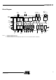
AT89C5131 XTAL1 XTAL2 EUART + BRG ALE RAM 256x8 EEPROM XRAM 4Kx8 1Kx8 32Kx8 Flash (1) (1) (1) (1) (1) (1) PCA SCK MISO MOSI T2 T2EX CEX ECI VDD VSS TxD (1) (1) (2) (2) SS RxD Block Diagram SPI Timer2 C51 CORE PSEN CPU EA Timer 0 Timer 1 (2) Notes: INT Ctrl Parallel I/O Ports & Ext. Bus Key Watch USB Board Dog Regulator VREF AVDD AVSS D+ D- KIN P4 P3 P2 P1 P0 INT1 (2) (2) T1 (2) (2) INT0 Port 0 Port 1 Port 2 Port 3 Port 4 RST WR (2) T0 RD 1.
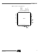
Pinout Description Pinout P4.1 P2.3/A11 P1.0/T2/KIN0 P1.2/ECI/KIN2 1 52 51 50 49 48 47 P1.1/T2EX/KIN1/SS P2.0/A8 2 P1.4/CEX1/KIN4 P2.1/A9 3 P1.3/CEX0/KIN3 P2.2/A10 5 4 P0.0/AD0 P1.6/CEX3/KIN6/SCK 6 8 46 NC 9 P0.1/AD1 P2.4/A12 10 45 44 P2.5/A13 11 43 XTAL2 42 XTAL1 12 13 P2.6/A14 14 P2.7/A15 VDD P0.2/AD2 RST P0.3/AD3 41 VSS P0.4/AD4 15 40 39 16 38 P0.5/AD5 AVDD 17 37 P0.6/AD6 PLCC52 P3.7/RD/LED3 NC 18 36 P0.7/AD7 AVSS 19 35 P3.6/WR/LED2 P3.
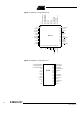
AT89C5131 NC P1.0/T2/KIN0 P1.2/ECI/KIN2 P1.1/T2EX/KIN1/SS P1.3/CEX0/KIN3 P0.0/AD0 P1.4/CEX1/KIN4 P2.1/A9 P2.0/A8 P2.2/A10 P1.5/CEX2/KIN5/MISO P1.6/CEX3/KIN6/SCK NC P4.1 P4.0 P1.7/CEX4/KIN7/MOSI Figure 2. AT89C5131 64-pin VQFP Pinout 64 63 62 61 60 59 58 57 56 55 54 53 52 51 50 49 NC P2.3/A11 1 2 48 47 NC P2.4/A12 3 46 P0.1/AD1 P2.5/A13 4 45 P0.2/AD2 XTAL2 XTAL1 5 6 44 43 RST P0.3/AD3 VSS P2.6/A14 7 42 P2.7/A15 VDD AVDD 8 9 41 40 VQFP64 10 39 11 AVSS 12 NC 13 P3.
P1.2/ECI/KIN2 P1.1/T2EX/KIN1/SS P1.4/CEX1/KIN4 P1.3/CEX0/KIN3 P2.0/A8 P0.0/AD0 P2.1/A9 P2.2/A10 P1.6/CEX3/KIN6/SCK P1.5/CEX2/KIN5/MISO P4.0 P1.7/CEX4/KIN7/MOSI Figure 3. AT89C5131 48-pin MLF Pinout 48 47 46 45 44 43 42 41 40 39 38 37 P4.1 P2.3/A11 1 36 P1.0/T2/KIN0 2 35 P0.1/AD1 P2.4/A12 3 34 P0.2/AD2 P2.5/A13 4 33 XTAL2 5 6 32 RST P0.3/AD3 XTAL1 31 VSS P0.4/AD4 8 30 29 9 28 P0.5/AD5 27 P0.6/AD6 MLF 48 P2.6/A14 P2.7/A15 7 VDD AVDD 10 AVSS 11 26 P0.7/AD7 P3.
AT89C5131 Signals All the AT89C5131 signals are detailed by functionality on Table 1 through Table 11. Table 1. Keypad Interface Signal Description Signal Name Type KIN[7:0) I Description Keypad Input Lines Holding one of these pins high or low for 24 oscillator periods triggers a keypad interrupt if enabled. Held line is reported in the KBCON register. Alternate Function P1[7:0] Table 2.
Table 4. Timer 0, Timer 1 and Timer 2 Signal Description (Continued) Signal Name Type T0 I Timer Counter 0 External Clock Input When Timer 0 operates as a counter, a falling edge on the T0 pin increments the count. P3.4 T1 I Timer/Counter 1 External Clock Input When Timer 1 operates as a counter, a falling edge on the T1 pin increments the count. P3.
AT89C5131 Table 7. Ports Signal Description Signal Name P0[7:0] P1[7:0] P2[7:0] Type Description I/O Port 0 P0 is an 8-bit open-drain bidirectional I/O port. Port 0 pins that have 1s written to them float and can be used as high impedance inputs. To avoid any parasitic current consumption, Floating P0 inputs must be pulled to VDD or VSS. I/O Port 1 P1 is an 8-bit bidirectional I/O port with internal pull-ups, except for P1.6 and P1.7 that are true open drain outputs.
Table 10. System Signal Description Signal Name Type AD[7:0] I/O A[15:8] I/O RD I/O Alternate Function Description Multiplexed Address/Data LSB for external access P0[7:0] Data LSB for Slave port access (used for 8-bit and 16-bit modes) Address Bus MSB for external access P2[7:0] Data MSB for Slave port access (used for 16-bit mode only) Read Signal Read signal asserted during external data memory read operation. P3.7 Control input for slave port read access cycles.
AT89C5131 Table 11. Power Signal Description (Continued) Signal Name Type Description Alternate Function 3V Voltage Reference VREF is used to supply the on-chip USB differential drivers. VREF It is internally connected to the on-chip voltage regulator output of the PWR standard versions, which must be connected to an external decoupling capacitor and can be connected to D+ with a 15 kΩ resistor. - It must be provided from outside on the Low Power versions, which have no internal voltage regulator.
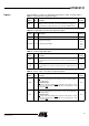
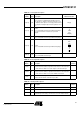
SFR Mapping 12 The Special Function Registers (SFRs) of the AT89C5131 fall into the following categories: • C51 core registers: ACC, B, DPH, DPL, PSW, SP • I/O port registers: P0, P1, P2, P3, P4 • Timer registers: T2CON, T2MOD, TCON, TH0, TH1, TH2, TMOD, TL0, TL1, TL2, RCAP2L, RCAP2H • Serial I/O port registers: SADDR, SADEN, SBUF, SCON • PCA (Programmable Counter Array) registers: CCON, CMOD, CCAPMx, CL, CH, CCAPxH, CCAPxL (x: 0 to 4) • Power and clock control registers: PCON • Hardware Watc
AT89C5131 The table below shows all SFRs with their address and their reset value. Table 12.
The Special Function Registers (SFRs) of the AT89C5131 fall into the following categories: Table 13. C51 Core SFRs Mnemonic Add Name ACC E0h Accumulator B F0h B Register PSW D0h Program Status Word SP 81h DPL 82h 7 6 5 4 3 2 1 0 7 6 5 4 3 2 1 0 Stack Pointer LSB of SPX Data Pointer Low byte LSB of DPTR DPH 83h Data Pointer High byte MSB of DPTR Table 14.
AT89C5131 Table 15.
Table 18.
AT89C5131 Table 21. Keyboard SFRs Mnemonic Add Name 7 6 5 4 3 2 1 0 KBF 9Eh Keyboard Flag Register KBF7 KBF6 KBF5 KBF4 KBF3 KBF2 KBF1 KBF0 KBE 9Dh Keyboard Input Enable Register KBE7 KBE6 KBE5 KBE4 KBE3 KBE2 KBE1 KBE0 KBLS 9Ch Keyboard Level Selector Register KBLS7 KBLS6 KBLS5 KBLS4 KBLS3 KBLS2 KBLS1 KBLS0 7 6 5 4 3 2 1 0 Table 22.
Table 24.
AT89C5131 Clock Controller Introduction The AT89C5131 clock controller is based on an on-chip oscillator feeding an on-chip Phase Lock Loop (PLL). All the internal clocks to the peripherals and CPU core are generated by this controller. The AT89C5131 X1 and X2 pins are the input and the output of a single-stage on-chip inverter (see Figure 5) that can be configured with off-chip components as a Pierce oscillator (see Figure 6).
Figure 6. Crystal Connection X1 C1 Q C2 VSS X2 PLL PLL Description The AT89C5131 PLL is used to generate internal high frequency clock (the USB Clock) synchronized with an external low-frequency (the Peripheral Clock). The PLL clock is used to generate the USB interface clock. Figure 7 shows the internal structure of the PLL. The PFLD block is the Phase Frequency Comparator and Lock Detector.
AT89C5131 PLL Programming The PLL is programmed using the flow shown in Figure 9. As soon as clock generation is enabled user must wait until the lock indicator is set to ensure the clock output is stable. Figure 9. PLL Programming Flow PLL Programming Configure Dividers N3:0 = xxxxb R3:0 = xxxxb Enable PLL PLLEN = 1 PLL Locked? LOCK = 1? Divider Values To generate a 48 MHz clock using the PLL, the divider values have to be configured following the oscillator frequency.
Registers Table 26. CKCON0 (S:8Fh) Clock Control Register 0 7 6 5 4 3 2 1 0 - WDX2 PCAX2 SIX2 T2X2 T1X2 T0X2 X2 Bit Bit Number Mnemonic Description 7 6 5 4 3 2 1 0 - Reserved The value read from this bit is always 0. Do not set this bit. WDX2 Watchdog Clock This control bit is validated when the CPU clock X2 is set. When X2 is low, this bit has no effect. Clear to select 6 clock periods per peripheral clock cycle. Set to select 12 clock periods per peripheral clock cycle.
AT89C5131 Table 27. CKCON1 (S:AFh) Clock Control Register 1 7 6 5 4 3 2 1 0 - - - - - - - SPIX2 Bit Bit Number Mnemonic Description 7-1 0 - SPIX2 Reserved The value read from this bit is always 0. Do not set this bit. SPI Clock This control bit is validated when the CPU clock X2 is set. When X2 is low, this bit has no effect. Clear to select 6 clock periods per peripheral clock cycle. Set to select 12 clock periods per peripheral clock cycle. Reset Value = 0000 0000b Table 28.
Dual Data Pointer Register The additional data pointer can be used to speed up code execution and reduce code size. The dual DPTR structure is a way by which the chip will specify the address of an external data memory location. There are two 16-bit DPTR registers that address the external memory, and a single bit called DPS = AUXR1.0 (see Table 30) that allows the program code to switch between them (see Figure 10). Figure 10.
AT89C5131 ASSEMBLY LANGUAGE ; Block move using dual data pointers ; Modifies DPTR0, DPTR1, A and PSW ; note: DPS exits opposite of entry state ; unless an extra INC AUXR1 is added ; 00A2 AUXR1 EQU 0A2H ; 0000 909000MOV DPTR,#SOURCE ; address of SOURCE 0003 05A2 INC AUXR1 ; switch data pointers 0005 90A000 MOV DPTR,#DEST ; address of DEST 0008 LOOP: 0008 05A2 INC AUXR1 ; switch data pointers 000A E0 MOVX A,@DPTR ; get a byte from SOURCE 000B A3 INC DPTR ; increment SOURCE address 000C 05A2 INC AUXR1 ; switch
Program/Code Memory The AT89C5131 implement 32 Kbytes of on-chip program/code memory. Figure 11 shows the split of internal and external program/code memory spaces depending on the product. The Flash memory increases EPROM and ROM functionality by in-circuit electrical erasure and programming. Thanks to the internal charge pump, the high voltage needed for programming or erasing Flash cells is generated on-chip using the standard VDD voltage.
AT89C5131 Table 31. External Data Memory Interface Signals External Bus Cycles Signal Name Type Alternate Function A15:8 O Address Lines Upper address lines for the external bus. P2.7:0 AD7:0 I/O Address/Data Lines Multiplexed lower address lines and data for the external memory. P0.7:0 ALE O Address Latch Enable ALE signals indicates that valid address information are available on lines AD7:0.
Figure 14. Flash Memory Architecture 3 Kbytes Flash Memory Boot Space Hardware Security (1 Byte) Extra Row (128 Bytes) Column Latches (128 Bytes) FM1 7FFFh 32 Kbytes FFFFh F400h FM1 mapped between FFFFh and F400h when bit ENBOOT is set in AUXR1 register Flash Memory User Space FM0 0000h FM0 Memory Architecture The Flash memory is made up of 4 blocks (see Figure 14): 1. The memory array (user space) 32 Kbytes 2. The Extra Row 3. The Hardware security bits 4.
AT89C5131 The other memory spaces (user, extra row, hardware security) are made accessible in the code segment by programming bits FMOD0 and FMOD1 in FCON register in accordance with Table 32. A MOVC instruction is then used for reading these spaces. Table 32.
Loading the Column Latches Any number of data from 1 byte to 128 bytes can be loaded in the column latches. This provides the capability to program the whole memory by byte, by page or by any number of bytes in a page. When programming is launched, an automatic erase of the locations loaded in the column latches is first performed, then programming is effectively done. Thus, no page or block erase is needed and only the loaded data are programmed in the corresponding page.
AT89C5131 Extra Row The following procedure is used to program the Extra Row space and is summarized in Figure 16: • Load data in the column latches from address FF80h to FFFFh. • Disable the interrupts. • Launch the programming by writing the data sequence 52h followed by A2h in FCON register. The end of the programming indicated by the FBUSY flag cleared. • Enable the interrupts. Figure 16.
Hardware Security The following procedure is used to program the Hardware Security space and is summarized in Figure 17: • Set FPS and map Hardware byte (FCON = 0x0C) • Disable the interrupts. • Load DPTR at address 0000h. • Load Accumulator register with the data to load. • Execute the MOVX @DPTR, A instruction. • Launch the programming by writing the data sequence 54h followed by A4h in FCON register. The end of the programming indicated by the FBusy flag cleared. • Enable the interrupts.
AT89C5131 Reading the Flash Spaces User Extra Row Hardware Security The following procedure is used to read the User space and is summarized in Figure 18: • Map the User space by writing 00h in FCON register. • Read one byte in Accumulator by executing MOVC A, @A+DPTR with A = 0 & DPTR = 0000h to FFFFh. The following procedure is used to read the Extra Row space and is summarized in Figure 18: • Map the Extra Row space by writing 02h in FCON register.
Registers Table 34. FCON (S:D1h) Flash Control Register 7 6 5 4 3 2 1 0 FPL3 FPL2 FPL1 FPL0 FPS FMOD1 FMOD0 FBUSY Bit Bit Number Mnemonic Description 7-4 FPL3:0 3 FPS 2-1 FMOD1:0 0 FBUSY Programming Launch Command Bits Write 5Xh followed by AXh to launch the programming according to FMOD1:0. (see Table 33.) Flash Map Program Space Set to map the column latch space in the data memory space. Clear to re-map the data memory space. Flash Mode See Table 32 or Table 33.
AT89C5131 Flash EEPROM Memory General Description The Flash memory increases EPROM functionality with in-circuit electrical erasure and programming. It contains 32 Kbytes of program memory organized in 256 pages of 128 bytes, respectively. This memory is both parallel and serial In-System Programmable (ISP). ISP allows devices to alter their own program memory in the actual end product under software control. A default serial loader (bootloader) program allows ISP of the Flash.
Flash Registers and Memory Map Hardware Registers The AT89C5131 Flash memory uses several registers: • Hardware registers can only be accessed through the parallel programming modes which are handled by the parallel programmer. • Software registers are in a special page of the Flash memory which can be accessed through the API or with the parallel programming modes. This page, called “Extra Flash Memory”, is not in the internal Flash program memory addressing space.
AT89C5131 Table 36. Program Lock bits Program Lock Bits Security level LB0 LB1 LB2 1 U U U No program lock features enabled. Notes: Protection Description 2 P U U MOVC instruction executed from external program memory is disabled from fetching code bytes from any internal memory, EA is sampled and latched on reset, and further parallel programming of the Flash and of the EEPROM (boot and Xdata) is disabled. ISP and software programming with API are still allowed.
Table 37.
AT89C5131 The two lock bits provide different levels of protection for the on-chip code and data, when programmed as shown to Table 39. Table 39. Program Lock Bits of the SSB Program Lock Bits Security Level LB0 LB1 1 U U No program lock features enabled. 2 P U ISP programming of the Flash is disabled. 3 X P Same as 2, also verify through ISP programming interface is disabled. Notes: Flash Memory Status 1. 2. 3. 4. Protection Description U: unprogrammed or "one" level.
Boot Process Boot Flash When the user application programs its own Flash memory, all of the low level details are handled by a code that is permanently contained in a 3 Kbyte “Boot ROM”. A user program simply calls the common entry point in the Boot ROM with appropriate parameters to accomplish the desired operation. Boot ROM operations include: erase block, program byte or page, verify byte or page, program security lock bit, etc.
AT89C5131 Figure 21.
In-System Programming (ISP) The In-System Programming (ISP) is performed without removing the microcontroller from the system. The ISP facility consists of a series of internal hardware resources coupled with internal firmware to facilitate remote programming of the AT89C5131 through the serial port. The Atmel ISP feature has made in-circuit programming in an embedded application possible with a minimum of additional expenses in components and circuit board area.
AT89C5131 Table 40. Intel-Hex Records Used by In-System Programming Record Type Command/Data Function Data Record :nnaaaa00dd....ddcc Where: Nn = number of bytes (hex) in record 00 aaaa = memory address of first byte in record dd....
Table 40.
AT89C5131 Table 40. Intel-Hex Records Used by In-System Programming (Continued) Record Type Command/Data Function Display Device Data or Blank Check Record type 04 causes the contents of the entire Flash array to be sent out the serial port in a formatted display. This display consists of an address and the contents of 16 bytes starting with that address. No display of the device contents will occur if security bit 2 has been programmed.
Table 41.
AT89C5131 Table 41.
Table 41.
AT89C5131 Table 41.
Table 41.
AT89C5131 EEPROM Data Memory Description The 1-Kbyte on-chip EEPROM memory block is located at addresses 0000h to 03FFh of the XRAM memory space and is selected by setting control bits in the EECON register. A read in the EEPROM memory is done with a MOVX instruction. A physical write in the EEPROM memory is done in two steps: write data in the column latches and transfer of all data latches into an EEPROM memory row (programming).
Registers Table 42. EECON (S:0D2h) EECON Register 7 6 5 4 3 2 1 0 EEPL3 EEPL2 EEPL1 EEPL0 - - EEE EEBUSY Bit Number Bit Mnemonic 7-4 EEPL3-0 Programming Launch command bits Write 5Xh followed by AXh to EEPL to launch the programming. 3 - Reserved The value read from this bit is indeterminate. Do not set this bit. 2 - Reserved The value read from this bit is indeterminate. Do not set this bit.
AT89C5131 In-System Programming (ISP) With the implementation of the User EEPROM and the Boot EEPROM in Flash technology the AT89C5131 allows the system engineer to develop applications with a very high level of flexibility.
Flash Programming and Erasure There are three methods of programming the Flash memory: • The Atmel bootloader located in FM1 is activated by the application. Low level API routines (located in FM1) to program FM0 will be used. The interface used for serial downloading to FM0 is the UART or the USB. API can be called also by user’s bootloader located in FM0 at [SBV]00h. • A further method exist for activating the Atmel bootloader by using hardware activation.
AT89C5131 WARNING: Security level 2 and 3 should only be programmed after Flash and Core verification. Program Lock Bits These security bits protect the code access through the parallel programming interface. They are set by default to level 4. Low Pin-count Boot Process The bootloader can be activated by two means: Regular boot process or Hardware condition. The hardware condition must be configured by the user using the P1_CF, P3_CF and P4_CF bytes.
Figure 23. Low Pin-count Boot Process Algorithm Hardware RESET BLJB = 1? F400h address 0000h address APPLICATION PROGRAM No P1_CF = FFh? Yes Software No P3_CF = FFh? Yes No No Yes Yes bit = = 0? No BSB = = 00h? P4_CF = FFh? SBV < 3Fh? Yes No Yes ATMEL BOOTLOADER APPLICATION PROGRAM CUSTOMER BOOTLOADER PC = [SBV]00h High Pin-Count Boot Process At the falling edge of RESET, the bit ENBOOT in AUXR1 register is initialized with the value of Bootloader Jump Bit (BLJB).
AT89C5131 • ALE high (or not connected) – After Hardware Condition the FCON register is initialized with the value 00h and the PC is initialized with F800h (FM1). The Hardware condition makes the bootloader to be executed, whatever BLJB value is. If no hardware condition is detected, the FCON register is initialized with the value F0h. Check of the BLJB value. • If bit BLJB = 1: User application in FM0 will be started at 0000h (standard reset).
Application Programming Interface Several Application Program Interface (API) calls are available for use by an application program to permit selective erasing and programming of Flash pages. All calls are made by functions. All these APIs will be described in an application note.
AT89C5131 XROW Bytes Table 44. XRow Mapping Mnemonic Description Default Value BSB Boot Status Byte SBV Software Boot Vector Address 00h F4h 01h P1_CF FFh 02h P3_CF FFh 03h P4_CF FFh 04h Software Security Byte FFh 05h Extra Byte FFh 06h SSB EB reserved ID1 07h-2Fh Manufacturer Code 58h 30h Device ID#1: Family code D7h 31h reserved 32h-5Fh ID2 Device ID#2: Memories size and type F7h 60h ID3 Device ID#3: Name and Revision DFh 61h reserved 62h-7Fh Table 45.
Hardware Byte Table 47. Hardware Byte 7 6 5 4 3 2 1 0 X2B BLJB OSCON1 OSCON0 - LB2 LB1 LB0 Bit Number Bit Mnemonic 7 X2B 6 BLJB Description X2 Bit Set this bit to start in standard mode Clear this bit to start in X2 mode. Bootloader Jump Bit Set this bit to start the user’s application on next reset at address 0000h. Cleared this bit to start the bootloader at address F400h (default).
AT89C5131 On-chip Expanded RAM (XRAM) The AT89C5131 provides additional Bytes of random access memory (RAM) space for increased data parameter handling and high level language usage. AT89C5131 devices have expanded RAM in external data space; maximum size and location are described in Table 48. Table 48. Description of Expanded RAM Address Part Number XRAM Size Start End AT89C5131 1024 00h 3FFh The AT89C5131 has on-chip data memory that is mapped into the following four separate segments. 1.
When an instruction accesses an internal location above address 7Fh, the CPU knows whether the access is to the upper 128 bytes of data RAM or to SFR space by the addressing mode used in the instruction. • Instructions that use direct addressing access SFR space. For example: MOV 0A0H, # data, accesses the SFR at location 0A0h (which is P2). • Instructions that use indirect addressing access the Upper 128 bytes of data RAM.
AT89C5131 Table 49. AUXR Register AUXR - Auxiliary Register (8Eh) 7 6 5 4 3 2 1 0 DPU - M0 - XRS1 XRS0 EXTRAM AO Bit Bit Number Mnemonic 7 DPU 6 - Description Disable Weak Pull Up Cleared to enabled weak pull up on standard Ports. Set to disable weak pull up on standard Ports. Reserved The value read from this bit is indeterminate. Do not set this bit Pulse length 5 M0 Cleared to stretch MOVX control: the RD and the WR pulse length is 6 clock periods (default).
Timer 2 The Timer 2 in the AT89C5131 is the standard C52 Timer 2. It is a 16-bit timer/counter: the count is maintained by two cascaded eight-bit timer registers, TH2 and TL2. It is controlled by T2CON (Table 50) and T2MOD (Table 51) registers. Timer 2 operation is similar to Timer 0 and Timer 1. C/T2 selects FOSC/12 (timer operation) or external pin T2 (counter operation) as the timer clock input. Setting TR2 allows TL2 to be incremented by the selected input.
AT89C5131 Figure 26. Auto-reload Mode Up/Down Counter (DCEN = 1) FCLK PERIPH :6 0 1 T2 C/T2 TR2 T2CON T2CON (DOWN COUNTING RELOAD VALUE) T2EX: FFh (8-bit) FFh (8-bit) if DCEN = 1, 1 = UP if DCEN = 1, 0 = DOWN if DCEN = 0, up counting TOGGLE T2CON EXF2 TL2 (8-bit) TH2 (8-bit) TF2 Timer 2 INTERRUPT T2CON RCAP2L (8-bit) RCAP2H (8-bit) (UP COUNTING RELOAD VALUE) Programmable Clock Output In the Clock-out mode, Timer 2 operates as a 50%-duty-cycle, programmable clock generator (See Figure 27).
It is possible to use Timer 2 as a baud rate generator and a clock generator simultaneously. For this configuration, the baud rates and clock frequencies are not independent since both functions use the values in the RCAP2H and RCAP2L registers. Figure 27.
AT89C5131 Table 50. T2CON Register T2CON - Timer 2 Control Register (C8h) 7 6 5 4 3 2 1 0 TF2 EXF2 RCLK TCLK EXEN2 TR2 C/T2# CP/RL2# Bit Bit Number Mnemonic 7 TF2 Description Timer 2 overflow Flag Must be cleared by software. Set by hardware on Timer 2 overflow, if RCLK = 0 and TCLK = 0. 6 EXF2 Timer 2 External Flag Set when a capture or a reload is caused by a negative transition on T2EX pin if EXEN2 = 1.
Table 51. T2MOD Register T2MOD - Timer 2 Mode Control Register (C9h) 7 6 5 4 3 2 1 0 - - - - - - T2OE DCEN Bit Number Bit Mnemonic Description 7 - Reserved The value read from this bit is indeterminate. Do not set this bit. 6 - Reserved The value read from this bit is indeterminate. Do not set this bit. 5 - Reserved The value read from this bit is indeterminate. Do not set this bit. 4 - Reserved The value read from this bit is indeterminate. Do not set this bit.
AT89C5131 Programmable Counter Array (PCA) The PCA provides more timing capabilities with less CPU intervention than the standard timer/counters. Its advantages include reduced software overhead and improved accuracy. The PCA consists of a dedicated timer/counter which serves as the time base for an array of five compare/capture modules.
Figure 28. PCA Timer/Counter To PCA modules FCLK PERIPH/6 overflow FCLK PERIPH/2 CH T0 OVF It CL 16 Bit Up/Down Counter P1.2 CIDL WDTE CF CR CPS1 CPS0 ECF CMOD 0xD9 CCF2 CCF1 CCF0 CCON 0xD8 Idle CCF4 CCF3 Table 52. CMOD Register CMOD - PCA Counter Mode Register (D9h) 7 6 5 4 3 2 1 0 CIDL WDTE - - - CPS1 CPS0 ECF Bit Bit Number Mnemonic 7 CIDL Description Counter Idle Control Cleared to program the PCA Counter to continue functioning during idle Mode.
AT89C5131 The CMOD register includes three additional bits associated with the PCA (See Figure 28 and Table 52). • The CIDL bit allows the PCA to stop during idle mode. • The WDTE bit enables or disables the watchdog function on module 4. • The ECF bit when set causes an interrupt and the PCA overflow flag CF (in the CCON SFR) to be set when the PCA timer overflows. The CCON register contains the run control bit for the PCA and the flags for the PCA timer (CF) and each module (see Table 53).
The watchdog timer function is implemented in module 4 (See Figure 31). The PCA interrupt system is shown in Figure 29. Figure 29. PCA Interrupt System CF CR CCF4 CCF3 CCF2 CCF1 CCF0 CCON 0xD8 PCA Timer/Counter Module 0 Module 1 To Interrupt priority decoder Module 2 Module 3 Module 4 CMOD.0 ECF ECCFn CCAPMn.0 IE.6 EC IE.7 EA PCA Modules: each one of the five compare/capture modules has six possible functions.
AT89C5131 the CAPP bit enables the positive edge. If both bits are set both edges will be enabled and a capture will occur for either transition. • The last bit in the register ECOM (CCAPMn.6) when set enables the comparator function. Table 55 shows the CCAPMn settings for the various PCA functions. Table 54.
Table 55. PCA Module Modes (CCAPMn Registers) ECOMn CAPPn CAPNn MATn TOGn PWM m ECCF n Module Function 0 0 0 0 0 0 0 No Operation X 1 0 0 0 0 X 16-bit capture by a positiveedge trigger on CEXn X 0 1 0 0 0 X 16-bit capture by a negative trigger on CEXn X 1 1 0 0 0 X 16-bit capture by a transition on CEXn 1 0 0 1 0 0 X 16-bit Software Timer/Compare mode.
AT89C5131 Table 56.
Table 59. CL Register CL - PCA Counter Register Low (0E9h) 7 6 5 4 3 2 1 0 - - - - - - - - Bit Bit Number Mnemonic 7-0 - Description PCA Counter CL Value Reset Value = 0000 0000b Not bit addressable PCA Capture Mode To use one of the PCA modules in the capture mode either one or both of the CCAPM bits CAPN and CAPP for that module must be set. The external CEX input for the module (on port 1) is sampled for a transition.
AT89C5131 Figure 31. PCA Compare Mode and PCA Watchdog Timer CCON CF Write to CCAPnL CR CCF4 CCF3 CCF2 CCF1 CCF0 0xD8 Reset PCA IT Write to CCAPnH 1 CCAPnH 0 CCAPnL Enable Match 16-bit Comparator CH RESET(1) CL PCA Counter/Timer ECOMn CAPPn CAPNn MATn TOGn PWMn ECCFn CIDL Note: WDTE CPS1 CPS0 ECF CCAPMn, n = 0 to 4 0xDA to 0xDE CMOD 0xD9 1. Only for Module 4 Before enabling ECOM bit, CCAPnL and CCAPnH should be set with a non zero value, otherwise an unwanted match could happen.
Figure 32. PCA High-speed Output Mode CCON CF CR CCF4 CCF3 CCF2 CCF1 CCF0 0xD8 Write to CCAPnL Reset PCA IT Write to CCAPnH 1 CCAPnH 0 CCAPnL Enable 16-bit Comparator CH Match CL CEXn PCA counter/timer ECOMn CAPPn CAPNn MATn TOGn PWMn ECCFn CCAPMn, n = 0 to 4 0xDA to 0xDE Before enabling ECOM bit, CCAPnL and CCAPnH should be set with a non zero value, otherwise an unwanted match could happen.
AT89C5131 Figure 33. PCA PWM Mode CCAPnH Overflow CCAPnL “0” Enable 8-bit Comparator < ≥ CEXn “1” CL PCA Counter/Timer ECOMn CAPPn CAPNn MATn TOGn PWMn ECCFn CCAPMn, n = 0 to 4 0xDA to 0xDE PCA Watchdog Timer An on-board watchdog timer is available with the PCA to improve the reliability of the system without increasing chip count. Watchdog timers are useful for systems that are susceptible to noise, power glitches, or electrostatic discharge.
Serial I/O Port The serial I/O port in the AT89C5131 is compatible with the serial I/O port in the 80C52. It provides both synchronous and asynchronous communication modes. It operates as an Universal Asynchronous Receiver and Transmitter (UART) in three full-duplex modes (modes 1, 2 and 3). Asynchronous transmission and reception can occur simultaneously and at different baud rates.
AT89C5131 Figure 36. UART Timings in Modes 2 and 3 RXD D0 Start Bit D1 D2 D3 D4 Data Byte D5 D6 D7 D8 Ninth Stop Bit Bit RI SMOD0 = 0 RI SMOD0 = 1 FE SMOD0 = 1 Automatic Address Recognition The automatic address recognition feature is enabled when the multiprocessor communication feature is enabled (SM2 bit in SCON register is set).
The SADEN byte is selected so that each slave may be addressed separately. For slave A, bit 0 (the LSB) is a don’t care bit; for slaves B and C, bit 0 is a 1. To communicate with slave A only, the master must send an address where bit 0 is clear (e.g. 1111 0000b). For slave A, bit 1 is a 1; for slaves B and C, bit 1 is a don’t care bit. To communicate with slaves B and C, but not slave A, the master must send an address with bits 0 and 1 both set (e.g. 1111 0011b).
AT89C5131 SADDR - Slave Address Register (A9h) 7 6 5 4 3 2 1 0 Reset Value = 0000 0000b Not bit addressable Baud Rate Selection for UART for Mode 1 and 3 The Baud Rate Generator for transmit and receive clocks can be selected separately via the T2CON and BDRCON registers. Figure 37.
Figure 38.
AT89C5131 Table 60. SCON Register – SCON Serial Control Register (98h) 7 6 5 4 3 2 1 0 FE/SM0 SM1 SM2 REN TB8 RB8 TI RI Bit Bit Number Mnemonic FE Description Framing Error bit (SMOD0 = 1) Clear to reset the error state, not cleared by a valid stop bit. Set by hardware when an invalid stop bit is detected. SMOD0 must be set to enable access to the FE bit 7 SM0 Serial port Mode bit 0 Refer to SM1 for serial port mode selection.
Example of computed value when X2 = 1, SMOD1 = 1, SPD = 1 FOSCA = 16.384 MHz Baud Rates FOSCA = 24 MHz BRL Error (%) BRL Error (%) 115200 247 1.23 243 0.16 57600 238 1.23 230 0.16 38400 229 1.23 217 0.16 28800 220 1.23 204 0.16 19200 203 0.63 178 0.16 9600 149 0.31 100 0.16 4800 43 1.23 - - Example of computed value when X2 = 0, SMOD1 = 0, SPD = 0 FOSCA = 16.384 MHz FOSCA = 24 MHz Baud Rates BRL Error (%) BRL Error (%) 4800 247 1.23 243 0.
AT89C5131 BRL - Baud Rate Reload Register for the internal baud rate generator, UART (9Ah) 7 6 5 4 3 2 1 0 – – – – – – – – Reset Value = 0000 0000b Table 61. T2CON Register T2CON - Timer 2 Control Register (C8h) 7 6 5 4 3 2 1 0 TF2 EXF2 RCLK TCLK EXEN2 TR2 C/T2# CP/RL2# Bit Bit Number Mnemonic 7 TF2 Description Timer 2 overflow Flag Must be cleared by software. Set by hardware on Timer 2 overflow, if RCLK = 0 and TCLK = 0.
Table 62. PCON Register PCON - Power Control Register (87h) 7 6 5 4 3 2 1 0 SMOD1 SMOD0 - POF GF1 GF0 PD IDL Bit Bit Number Mnemonic 7 SMOD1 6 SMOD0 5 - Description Serial port Mode bit 1 for UART Set to select double baud rate in mode 1, 2 or 3. Serial port Mode bit 0 for UART Cleared to select SM0 bit in SCON register. Set to select FE bit in SCON register. Reserved The value read from this bit is indeterminate. Do not set this bit.
AT89C5131 Table 63. BDRCON Register BDRCON - Baud Rate Control Register (9Bh) 7 6 5 4 3 2 1 0 - - - BRR TBCK RBCK SPD SRC Bit Number Bit Mnemonic 7 - Reserved The value read from this bit is indeterminate. Do not set this bit 6 - Reserved The value read from this bit is indeterminate. Do not set this bit 5 - Reserved The value read from this bit is indeterminate. Do not set this bit. 4 BRR Baud Rate Run Control bit Cleared to stop the internal Baud Rate Generator.
Interrupt System Overview The AT89C5131 has a total of 15 interrupt vectors: two external interrupts (INT0 and INT1), three timer interrupts (timers 0, 1 and 2), the serial port interrupt, SPI interrupt, Keyboard interrupt, USB interrupt and the PCA global interrupt. These interrupts are shown in Figure 39. Figure 39.
AT89C5131 Each of the interrupt sources can be individually enabled or disabled by setting or clearing a bit in the Interrupt Enable register (Table 65). This register also contains a global disable bit, which must be cleared to disable all interrupts at once. Each interrupt source can also be individually programmed to one out of four priority levels by setting or clearing a bit in the Interrupt Priority register (Table 66.) and in the Interrupt Priority High register (Table 67). Table 64.
Table 65. IE0 Register IE0 - Interrupt Enable Register (A8h) 7 6 5 4 3 2 1 0 EA EC ET2 ES ET1 EX1 ET0 EX0 Bit Bit Number Mnemonic 7 EA 6 EC Description Enable All interrupt bit Cleared to disable all interrupts. Set to enable all interrupts. PCA interrupt enable bit Cleared to disable. Set to enable. 5 ET2 Timer 2 overflow interrupt Enable bit Cleared to disable Timer 2 overflow interrupt. Set to enable Timer 2 overflow interrupt.
AT89C5131 Table 66. IPL0 Register IPL0 - Interrupt Priority Register (B8h) 7 6 5 4 3 2 1 0 - PPCL PT2L PSL PT1L PX1L PT0L PX0L Bit Bit Number Mnemonic 7 - 6 PPCL PCA interrupt Priority bit Refer to PPCH for priority level. 5 PT2L Timer 2 overflow interrupt Priority bit Refer to PT2H for priority level. 4 PSL Serial port Priority bit Refer to PSH for priority level. 3 PT1L Timer 1 overflow interrupt Priority bit Refer to PT1H for priority level.
Table 67. IPH0 Register IPH0 - Interrupt Priority High Register (B7h) 7 6 5 4 3 2 1 0 - PPCH PT2H PSH PT1H PX1H PT0H PX0H Bit Bit Number Mnemonic 7 - 6 5 4 3 2 1 0 Description Reserved The value read from this bit is indeterminate. Do not set this bit. PPCH PCA interrupt Priority high bit.
AT89C5131 Table 68. IE1 Register IE1 - Interrupt Enable Register (B1h) 7 6 5 4 3 2 1 0 - EUSB - - - ESPI - EKB Bit Bit Number Mnemonic 7 - 6 EUSB 5 - Reserved 4 - Reserved 3 - Reserved 2 ESPI 1 - 0 EKB Description Reserved USB Interrupt Enable bit SPI interrupt Enable bit Cleared to disable SPI interrupt. Set to enable SPI interrupt. Reserved Keyboard interrupt Enable bit Cleared to disable keyboard interrupt. Set to enable keyboard interrupt.
Table 69. IPL1 Register IPL1 - Interrupt Priority Register (B2h) 7 6 5 4 3 2 - PUSBL - - - PSPIL 1 Bit Bit Number Mnemonic 7 - Reserved The value read from this bit is indeterminate. Do not set this bit. 6 PUSBL USB Interrupt Priority bit The value read from this bit is indeterminate. Do not set this bit. 5 - Reserved The value read from this bit is indeterminate. Do not set this bit. 4 - Reserved The value read from this bit is indeterminate. Do not set this bit.
AT89C5131 Table 70. IPH1 Register IPH1 - Interrupt Priority High Register (B3h) 7 6 5 4 3 2 1 0 - - - - - PSPIH - PKBH Bit Bit Number Mnemonic 7 - Reserved The value read from this bit is indeterminate. Do not set this bit. 6 PUSBH USB Interrupt Priority High bit The value read from this bit is indeterminate. Do not set this bit. 5 - Reserved The value read from this bit is indeterminate. Do not set this bit. 4 - Reserved The value read from this bit is indeterminate.
Interrupt Sources and Vector Addresses 98 Table 71.
AT89C5131 Keyboard Interface Introduction The AT89C5131 implements a keyboard interface allowing the connection of a 8 x n matrix keyboard. It is based on 8 inputs with programmable interrupt capability on both high or low level. These inputs are available as an alternate function of P1 and allow to exit from idle and power down modes.
Power Reduction Mode P1 inputs allow exit from idle and power down modes as detailed in section “Powerdown Mode”. Registers Table 72. KBF Register KBF - Keyboard Flag Register (9Eh) 7 6 5 4 3 2 1 0 KBF7 KBF6 KBF5 KBF4 KBF3 KBF2 KBF1 KBF0 Bit Number 7 6 5 4 3 2 1 0 Bit Mnemonic Description KBF7 Keyboard line 7 flag Set by hardware when the Port line 7 detects a programmed level. It generates a Keyboard interrupt request if the KBKBIE.7 bit in KBIE register is set.
AT89C5131 Table 73. KBE Register KBE - Keyboard Input Enable Register (9Dh) 7 6 5 4 3 2 1 0 KBE7 KBE6 KBE5 KBE4 KBE3 KBE2 KBE1 KBE0 Bit Number Bit Mnemonic Description 7 KBE7 Keyboard line 7 Enable bit Cleared to enable standard I/O pin. Set to enable KBF.7 bit in KBF register to generate an interrupt request. 6 KBE6 Keyboard line 6 Enable bit Cleared to enable standard I/O pin. Set to enable KBF.6 bit in KBF register to generate an interrupt request.
Table 74. KBLS Register KBLS-Keyboard Level Selector Register (9Ch) 7 6 5 4 3 2 1 0 KBLS7 KBLS6 KBLS5 KBLS4 KBLS3 KBLS2 KBLS1 KBLS0 Bit Number Bit Mnemonic Description 7 KBLS7 Keyboard line 7 Level Selection bit Cleared to enable a low level detection on Port line 7. Set to enable a high level detection on Port line 7. 6 KBLS6 Keyboard line 6 Level Selection bit Cleared to enable a low level detection on Port line 6. Set to enable a high level detection on Port line 6.
AT89C5131 Programmable LED AT89C5131 have up to 4 programmable LED current sources, configured by the register LEDCON. Table 75. LEDCON Register LEDCON (S:F1h) LED Control Register 7 6 5 LED3 Bit Number 7:6 5:4 3:2 1:0 4 LED2 Bit Mnemonic 3 2 LED1 1 0 LED0 Description LED3 Port 0 0 1 1 LED0 0 1 0 1 Configuration Standard C51 Port 2 mA current source when P3.7 is O 4 mA current source when P3.7 is O 10 mA current source when P3.
Serial Peripheral Interface (SPI) The Serial Peripheral Interface module (SPI) allows full-duplex, synchronous, serial communication between the MCU and peripheral devices, including other MCUs.
AT89C5131 pins (Figure 42). To prevent bus conflicts on the MISO line, only one slave should be selected at a time by the Master for a transmission. In a Master configuration, the SS line can be used in conjunction with the MODF flag in the SPI Status register (SPSTA) to prevent multiple masters from driving MOSI and SCK (see Section “Error Conditions”, page 109). A high level on the SS pin puts the MISO line of a Slave SPI in a high-impedance state.
Functional Description Figure 43 shows a detailed structure of the SPI module. Figure 43.
AT89C5131 Figure 44. Full-duplex Master/Slave Interconnection 8-bit Shift Register SPI Clock Generator MISO MISO MOSI MOSI SCK SS Master MCU 8-bit Shift Register SCK VDD SS VSS Slave MCU Master Mode The SPI operates in Master mode when the Master bit, MSTR (1), in the SPCON register is set. Only one Master SPI device can initiate transmissions. Software begins the transmission from a Master SPI module by writing to the Serial Peripheral Data Register (SPDAT).
Figure 45. Data Transmission Format (CPHA = 0) SCK cycle number 1 2 3 4 5 6 7 8 MSB bit6 bit5 bit4 bit3 bit2 bit1 LSB bit6 bit5 bit4 bit3 bit2 bit1 LSB SPEN (internal) SCK (CPOL = 0) SCK (CPOL = 1) MOSI (from Master) MISO (from Slave) MSB SS (to Slave) Capture point Figure 46.
AT89C5131 Error Conditions The following flags in the SPSTA signal SPI error conditions: Mode Fault (MODF) Mode Fault error in Master mode SPI indicates that the level on the Slave Select (SS) pin is inconsistent with the actual mode of the device. MODF is set to warn that there may have a multi-master conflict for system control. In this case, the SPI system is affected in the following ways: • An SPI receiver/error CPU interrupt request is generated, • The SPEN bit in SPCON is cleared.
Figure 48. SPI Interrupt Requests Generation SPIF SPI Transmitter CPU Interrupt Request SPI CPU Interrupt Request MODF SPI Receiver/Error CPU Interrupt Request SSDIS Registers There are three registers in the module that provide control, status and data storage functions. These registers are describes in the following paragraphs.
AT89C5131 Bit Number 2 1 Bit Mnemonic Description SPR1 SPR0 SPR2 SPR1 SPR0 Serial Peripheral Rate 0 0 0 Invalid 0 0 1 FCLK PERIPH/4 0 1 0 FCLK PERIPH/8 0 1 1 FCLK PERIPH/16 1 0 0 FCLK PERIPH/32 1 0 1 FCLK PERIPH/64 1 1 0 FCLK PERIPH/128 1 1 1 Invalid Reset Value = 0001 0100b Not bit addressable Serial Peripheral Status Register (SPSTA) The Serial Peripheral Status Register contains flags to signal the following conditions: • Data transfer complete • Write collis
Bit Number Bit Mnemonic Description 2 - 1 - 0 - Reserved The value read from this bit is indeterminate. Do not set this bit Reserved The value read from this bit is indeterminate. Do not set this bit. Reserved The value read from this bit is indeterminate. Do not set this bit. Reset Value = 00X0 XXXXb Not Bit addressable Serial Peripheral Data Register (SPDAT) The Serial Peripheral Data Register (Table 80) is a read/write buffer for the receive data register.
AT89C5131 USB Controller Introduction The AT89C5131 implements a USB device controller supporting full speed data transfer.
USB Device Firmware Upgrade (DFU) The USB Device Firmware Update (DFU) protocol can be used to upgrade the on-chip Flash memory of the AT89C5131. This allows the implementation of product enhancements and patches to devices that are already in the field. Two different configurations and descriptor sets are used to support DFU functions. The Run-Time configuration coexists with the usual functions of the device, which may be USB Mass Storage for the AT89C5131.
AT89C5131 Serial Interface Engine (SIE) The SIE performs the following functions: • NRZI data encoding and decoding. • Bit stuffing and un-stuffing. • CRC generation and checking. • Handshakes. • TOKEN type identifying. • Address checking. • Clock generation (via DPLL). Figure 50.
Function Interface Unit (FIU) The Function Interface Unit provides the interface between the AT89C5131 and the SIE. It manages transactions at the packet level with minimal intervention from the device firmware, which reads and writes the endpoint FIFOs. Figure 51.
AT89C5131 Configuration General Configuration • USB controller enable Before any USB transaction, the 48 MHz required by the USB controller must be correctly generated (See “Clock Controller” on page 19). The USB controller will be then enabled by setting the EUSB bit in the USBCON register. • Set address After a Reset or a USB reset, the software has to set the FEN (Function Enable) bit in the USBADDR register. This action will allow the USB controller to answer to the requests sent at the address 0.
• Endpoint enable Before using an endpoint, this one will be enabled by setting the EPEN bit in the UEPCONX register. An endpoint which is not enabled won’t answer to any USB request. The Default Control Endpoint (Endpoint 0) will always be enabled in order to answer to USB standard requests. • Endpoint type configuration All Standard Endpoints can be configured in Control, Bulk, Interrupt or Isochronous mode. The Ping-pong Endpoints can be configured in Bulk, Interrupt or Isochronous mode.
AT89C5131 • Endpoint FIFO reset Before using an endpoint, its FIFO will be reset. This action resets the FIFO pointer to its original value, resets the byte counter of the endpoint (UBYCTLX and UBYCTHX registers), and resets the data toggle bit (DTGL bit in UEPCONX). The reset of an endpoint FIFO is performed by setting to 1 and resetting to 0 the corresponding bit in the UEPRST register. For example, in order to reset the Endpoint number 2 FIFO, write 0000 0100b then 0000 0000b in the UEPRST register.
Bulk/Interrupt Transactions Bulk and Interrupt transactions are managed in the same way. Bulk/Interrupt OUT Transactions in Standard Mode Figure 55.
AT89C5131 Bulk/Interrupt OUT Transactions in Ping-pong Mode Figure 56.
Bulk/Interrupt IN Transactions in Standard Mode Figure 57. Bulk/Interrupt IN Transactions in Standard Mode UFI HOST C51 Endpoint FIFO Write Byte 1 IN Endpoint FIFO Write Byte 2 NAK Endpoint FIFO Write Byte n Set TXRDY IN DATA0 (n Bytes) ACK TXCMPL Clear TXCMPL Endpoint FIFO Write Byte 1 An endpoint will be first enabled and configured before being able to send Bulk or Interrupt packets.
AT89C5131 Bulk/Interrupt IN Transactions in Ping-pong Mode Figure 58.
Control Transactions Setup Stage The DIR bit in the UEPSTAX register will be at 0. Receiving Setup packets is the same as receiving Bulk Out packets, except that the RXSETUP bit in the UEPSTAX register is set by the USB controller instead of the RXOUTB0 bit to indicate that an Out packet with a Setup PID has been received on the Control endpoint. When the RXSETUP bit has been set, all the other bits of the UEPSTAX register are cleared and an interrupt is triggered if enabled.
AT89C5131 Isochronous Transactions Isochronous OUT Transactions in Standard Mode An endpoint will be first enabled and configured before being able to receive Isochronous packets. When a OUT packet is received on an endpoint, the RXOUTB0 bit is set by the USB controller. This triggers an interrupt if enabled. The firmware has to select the corresponding endpoint, store the number of data bytes by reading the UBYCTLX and UBYCTHX registers.
If the Host sends more bytes than supported by the endpoint FIFO, the overflow data won’t be stored, but the USB controller will consider that the packet is valid if the CRC is correct. Isochronous IN Transactions in Standard Mode An endpoint will be first enabled and configured before being able to send Isochronous packets.
AT89C5131 Miscellaneous USB Reset The EORINT bit in the USBINT register is set by hardware when a End Of Reset has been detected on the USB bus. This triggers a USB interrupt if enabled. The USB controller is still enabled, but all the USB registers are reset by hardware. The firmware will clear the EORINT bit to allow the next USB reset detection. STALL Handshake This function is only available for Control, Bulk, and Interrupt endpoints.
Suspend/Resume Management Suspend The Suspend state can be detected by the USB controller if all the clocks are enabled and if the USB controller is enabled. The bit SPINT is set by hardware when an idle state is detected for more than 3 ms. This triggers a USB interrupt if enabled. In order to reduce current consumption, the firmware can stop the clocks and put the C51 in Idle or Power-down mode. The Resume detection is still active.
AT89C5131 Upstream Resume A USB device can be allowed by the Host to send an upstream resume for Remote Wake Up purpose. When the USB controller receives the SET_FEATURE request: DEVICE_REMOTE_WAKEUP, the firmware will set to 1 the RMWUPE bit in the USBCON register to enable this functionality. RMWUPE value will be 0 in the other cases.
Detach Simulation In order to be re-enumerated by the Host, the AT89C5131 has the possibility to simulate a DETACH - ATTACH of the USB bus. The VREF output voltage is between 3.0V and 3.6V. This output can be connected to the D+ pull-up as shown in Figure 61. This output can be put in high-impedance when the DETACH bit is set to 1 in the USBCON register. Maintaining this output in high impedance for more than 3 µs will simulate the disconnection of the device.
AT89C5131 Table 82. Priority Levels USB Interrupt Control System IPHUSB IPLUSB USB Priority Level 0 0 0 0 1 1 1 0 2 1 1 3 Lowest Highest As shown in Figure 64, many events can produce a USB interrupt: • TXCMPL: Transmitted In Data (see Table 89 on page 138). This bit is set by hardware when the Host accept a In packet. • RXOUTB0: Received Out Data Bank 0 (see Table 89 on page 138). This bit is set by hardware when an Out packet is accepted by the endpoint and stored in bank 0.
Figure 64. USB Interrupt Control Block Diagram Endpoint X (X = 0..6) TXCMP UEPSTAX.0 RXOUTB0 UEPSTAX.1 EPXINT UEPINT.X RXOUTB1 UEPSTAX.6 EPXIE UEPIEN.X RXSETUP UEPSTAX.2 STLCRC UEPSTAX.3 WUPCPU USBINT.5 EWUPCPU USBIEN.5 EUSB IE1.6 EORINT USBINT.4 EEORINT USBIEN.4 SOFINT USBINT.3 ESOFINT USBIEN.3 SPINT USBINT.0 ESPINT USBIEN.
AT89C5131 USB Registers Table 83. USBCON Register USBCON (S:BCh) USB Global Control Register 7 6 5 4 3 2 1 0 USBE SUSPCLK SDRMWUP DETACH UPRSM RMWUPE CONFG FADDEN Bit Number 7 6 5 4 3 2 Bit Mnemonic Description USBE USB Enable Set this bit to enable the USB controller. Clear this bit to disable and reset the USB controller, to disable the USB transceiver an to disable the USB controller clock inputs.
Table 84. USBINT Register USBINT (S:BDh) USB Global Interrupt Register 7 6 5 4 3 2 1 0 - - WUPCPU EORINT SOFINT - - SPINT Bit Bit Number Mnemonic Description 7-6 - Reserved The value read from these bits is always 0. Do not set these bits. 5 Wake Up CPU Interrupt This bit is set by hardware when the USB controller is in SUSPEND state and is re-activated by a non-idle signal FROM USB line (not by an upstream resume).
AT89C5131 Table 85. USBIEN Register USBIEN (S:BEh) USB Global Interrupt Enable Register 7 6 5 4 3 2 1 0 - - EWUPCPU EEORINT ESOFINT - - ESPINT Bit Number Bit Mnemonic Description 7-6 5 Reserved The value read from these bits is always 0. Do not set these bits. - EWUPCPU Enable Wake Up CPU Interrupt Set this bit to enable Wake Up CPU Interrupt. (See “USBIEN Register USBIEN (S:BEh) USB Global Interrupt Enable Register” on page 135) Clear this bit to disable Wake Up CPU Interrupt.
Table 87. UEPNUM Register UEPNUM (S:C7h) USB Endpoint Number 7 6 5 4 3 2 1 0 - - - - EPNUM3 EPNUM2 EPNUM1 EPNUM0 Bit Number Bit Mnemonic 7-4 - 3-0 EPNUM[3:0] Description Reserved The value read from these bits is always 0. Do not set these bits.
AT89C5131 Table 88. UEPCONX Register UEPCONX (S:D4h) USB Endpoint X Control Register 7 6 5 4 3 2 1 0 EPEN - - - DTGL EPDIR EPTYPE1 EPTYPE0 Bit Number Bit Mnemonic 7 EPEN 6-4 - 3 2 1-0 Note: Description Endpoint Enable Set this bit to enable the endpoint according to the device configuration. Endpoint 0 will always be enabled after a hardware or USB bus reset and participate in the device configuration. Clear this bit to disable the endpoint according to the device configuration.
Table 89. UEPSTAX (S:CEh) USB Endpoint X Status Register 7 6 5 4 3 2 1 0 DIR RXOUTB1 STALLRQ TXRDY STL/CRC RXSETUP RXOUTB0 TXCMP Bit Number Bit Mnemonic Description DIR Control Endpoint Direction This bit is used only if the endpoint is configured in the control type (seeSection “UEPCONX Register UEPCONX (S:D4h) USB Endpoint X Control Register”). This bit determines the Control data and status direction.
AT89C5131 Table 90. UEPDATX Register UEPDATX (S:CFh) USB FIFO Data Endpoint X (X = EPNUM set in UEPNUM Register UEPNUM (S:C7h) 7 6 5 4 3 2 1 0 FDAT7 FDAT6 FDAT5 FDAT4 FDAT3 FDAT2 FDAT1 FDAT0 Bit Bit Number Mnemonic Description Endpoint X FIFO data 7-0 FDAT[7:0] Data byte to be written to FIFO or data byte to be read from the FIFO, for the Endpoint X (see EPNUM). USB Endpoint Number) Reset Value = XXh Table 91.
Table 92. UBYCTHX Register UBYCTHX (S:E3h) USB Byte Count High Register X (X = EPNUM set in UEPNUM Register UEPNUM 7 6 5 4 3 2 1 0 - - - - - - BYCT9 BYCT8 Bit Number Bit Mnemonic Description 7-2 2-0 - BYCT[10:8] Reserved The value read from these bits is always 0. Do not set these bits. Byte Count MSB Most Significant Byte of the byte count of a received data packet.
AT89C5131 Table 93. UEPRST Register UEPRST (S:D5h) USB Endpoint FIFO Reset Register 7 6 5 4 3 2 1 0 - EP6RST EP5RST EP4RST EP3RST EP2RST EP1RST EP0RST Bit Bit Number Mnemonic Description Reserved The value read from this bit is always 0. Do not set this bit. 7 - 6 EP6RST Endpoint 6 FIFO Reset Set this bit and reset the endpoint FIFO prior to any other operation, upon hardware reset or when an USB bus reset has been received.
Table 94. UEPINT Register UEPINT (S:F8h read-only) USB Endpoint Interrupt Register 7 6 5 4 3 2 1 0 - EP6INT EP5INT EP4INT EP3INT EP2INT EP1INT EP0INT Bit Bit Number Mnemonic Description 7 6 5 4 3 2 1 0 - Reserved The value read from this bit is always 0. Do not set this bit.
AT89C5131 Table 95. UEPIEN Register UEPIEN (S:C2h) USB Endpoint Interrupt Enable Register 7 6 5 4 3 2 1 0 - EP6INTE EP5INTE EP4INTE EP3INTE EP2INTE EP1INTE EP0INTE Bit Bit Number Mnemonic Description Reserved The value read from this bit is always 0. Do not set this bit. 7 - 6 EP6INTE Endpoint 6 Interrupt Enable Set this bit to enable the interrupts for this endpoint. Clear this bit to disable the interrupts for this endpoint.
Table 96. UFNUMH Register UFNUMH (S:BBh, read-only) USB Frame Number High Register 7 6 5 4 3 2 1 0 - - CRCOK CRCERR - FNUM10 FNUM9 FNUM8 Bit Number Bit Mnemonic Description CRCOK Frame Number CRC OK This bit is set by hardware when a new Frame Number in Start of Frame Packet is received without CRC error. This bit is updated after every Start of Frame packet receipt. Important note: the Start of Frame interrupt is generated just after the PID receipt.
AT89C5131 Power Management Idle Mode An instruction that sets PCON.0 indicates that it is the last instruction to be executed before going into the Idle mode. In the Idle mode, the internal clock signal is gated off to the CPU, but not to the interrupt, Timer, and Serial Port functions. The CPU status is preserved in its entirety: the Stack Pointer, Program Counter, Program Status Word, Accumulator and all other registers maintain their data during Idle.
Figure 65. Power-down Exit Waveform INT0 INT1 XTALA or XTALB Power-down Phase Active Phase Oscillator restart Phase Active Phase Exit from power-down by reset redefines all the SFRs, exit from power-down by external interrupt does no affect the SFRs. Exit from power-down by either reset or external interrupt does not affect the internal RAM content.
AT89C5131 Registers Table 99. PCON Register PCON (S:87h) Power Control Register 7 6 5 4 3 2 1 0 SMOD1 SMOD0 - POF GF1 GF0 PD IDL Bit Bit Number Mnemonic Description 7 SMOD1 Serial Port Mode bit 1 Set to select double baud rate in mode 1, 2 or 3. 6 SMOD0 Serial Port Mode bit 0 Set to select FE bit in SCON register. Clear to select SM0 bit in SCON register 5 - Reserved The value read from this bit is always 0. Do not set this bit.
Hardware Watchdog Timer The WDT is intended as a recovery method in situations where the CPU may be subjected to software upset. The WDT consists of a 14-bit counter and the WatchDog Timer ReSeT (WDTRST) SFR. The WDT is by default disabled from exiting reset. To enable the WDT, user must write 01EH and 0E1H in sequence to the WDTRST, SFR location 0A6H.
AT89C5131 Table 101. WDTPRG Register WDTPRG - Watchdog Timer Out Register (0A7h) 7 6 5 4 3 2 1 0 - - - - - S2 S1 S0 Bit Bit Number Mnemonic 7 - 6 - 5 - 4 - 3 - 2 S2 WDT Time-out select bit 2 1 S1 WDT Time-out select bit 1 0 S0 WDT Time-out select bit 0 Description Reserved The value read from this bit is undetermined. Do not try to set this bit. S2 0 0 0 0 1 1 1 1 S1 0 0 1 1 0 0 1 1 S0 0 1 0 1 0 1 0 1 Selected Time-out (214 - 1) machine cycles, 16.
ONCE Mode (ON Chip Emulation) The ONCE mode facilitates testing and debugging of systems using AT89C5131 without removing the circuit from the board. The ONCE mode is invoked by driving certain pins of the AT89C5131; the following sequence must be exercised: • Pull ALE low while the device is in reset (RST high) and PSEN is high. • Hold ALE low as RST is deactivated.
AT89C5131 Reduced EMI Mode The ALE signal is used to demultiplex address and data buses on port 0 when used with external program or data memory. Nevertheless, during internal code execution, ALE signal is still generated. In order to reduce EMI, ALE signal can be disabled by setting AO bit. The AO bit is located in AUXR register at bit location 0. As soon as AO is set, ALE is no longer output but remains active during MOVX and MOVC instructions and external fetches.
Electrical Characteristics Absolute Maximum Ratings Note: Ambient Temperature Under Bias: I = industrial ........................................................-40°C to 85°C Storage Temperature .................................... -65°C to + 150°C Voltage on VCC from VSS ......................................-0.5V to + 6V Voltage on Any Pin from VSS .....................-0.5V to VCC + 0.2V Stresses at or above those listed under “Absolute Maximum Ratings” may cause permanent damage to the device.
AT89C5131 DC Parameters for Low Voltage TA = -40°C to +85°C; VSS = 0V; VCC = 3.3V ± 10%; F = 0 to 40 MHz Symbol Parameter Min VIL Input Low Voltage VIH Input High Voltage except XTAL1, RST VIH1 Input High Voltage, XTAL1, RST VOL Output Low Voltage, ports 1, 2, 3 and 4(6) VOL1 Output Low Voltage, port 0, ALE, PSEN VOH Output High Voltage, port 0, ALE, PSEN RRST Max Unit -0.5 0.2Vcc - 0.1 V 0.2 VCC + 0.9 VCC + 0.5 V 0.7 VCC VCC + 0.
6. Under steady state (non-transient) conditions, IOL must be externally limited as follows: Maximum IOL per port pin: 10 mA Maximum IOL per 8-bit port: Port 0: 26 mA Ports 1, 2 and 3: 15 mA Maximum total IOL for all output pins: 71 mA If IOL exceeds the test condition, VOL may exceed the related specification. Pins are not guaranteed to sink current greater than the listed test conditions. Figure 66.
AT89C5131 Figure 68. ICC Test Condition, Power-down Mode VCC ICC VCC VCC P0 VCC RST (NC) EA XTAL2 XTAL1 VSS All other pins are disconnected. Figure 69. Clock Signal Waveform for ICC Tests in Active and Idle Modes VCC-0.5V 0.45V TCLCH TCHCL TCLCH = TCHCL = 5ns. 0.7VCC 0.2VCC-0.
USB DC Parameters 1 - VBUS 2-D3-D+ 4 - GND R 3 2 USB “B” Receptacle VREF Rpad Rpad 4 D+ D- 1 R = 1.5 kΩ Rpad = 27Ω Symbol VREF 156 Parameter Min USB Reference Voltage 3.0 VIH Input High Voltage for D+ and D- (Driven) 2.0 VIHZ Input High Voltage for D+ and D- (Floating) 2.7 VIL Input Low Voltage for D+ and D- VOH Output High Voltage for D+ and D- VOL Output Low Voltage for D+ and D- Typ Max Unit 3.6 V V 3.6 V 0.8 V 2.8 3.6 V 0.0 0.
AT89C5131 AC Parameters Explanation of the AC Symbols Each timing symbol has 5 characters. The first character is always a “T” (stands for time). The other characters, depending on their positions, stand for the name of a signal or the logical status of that signal. The following is a list of all the characters and what they stand for. Example:TAVLL = Time for Address Valid to ALE Low. TLLPL = Time for ALE Low to PSEN Low. TA = -40°C to +85°C; VSS = 0V; VCC = 5V ±10%; F = 0 to 40 MHz.
Table 105. AC Parameters for a Fix Clock (F = 40 MHz) Symbol Min Max T 25 ns TLHLL 40 ns TAVLL 10 ns TLLAX 10 ns TLLIV Units 70 ns TLLPL 15 ns TPLPH 55 ns TPLIV 35 TPXIX ns 0 ns TPXIZ 18 ns TAVIV 85 ns TPLAZ 10 ns Table 106. AC Parameters for a Variable Clock 158 Symbol Type Standard Clock X2 Clock X Parameter Units TLHLL Min 2T-x T-x 10 ns TAVLL Min T-x 0.5 T - x 15 ns TLLAX Min T-x 0.
AT89C5131 External Program Memory Read Cycle 12 TCLCL TLHLL TLLIV ALE TLLPL TPLPH PSEN TLLAX TAVLL PORT 0 INSTR IN TPLIV TPLAZ A0-A7 TPXAV TPXIZ TPXIX INSTR IN A0-A7 INSTR IN TAVIV PORT 2 ADDRESS OR SFR-P2 External Data Memory Characteristics ADDRESS A8-A15 ADDRESS A8-A15 Table 107.
Table 108.
AT89C5131 Table 109. AC Parameters for a Variable Clock Symbol Type Standard Clock X2 Clock X Parameter Units TRLRH Min 6T-x 3T-x 20 ns TWLWH Min 6T-x 3T-x 20 ns TRLDV Max 5T-x 2.5 T - x 25 ns TRHDX Min x x 0 ns TRHDZ Max 2T-x T-x 20 ns TLLDV Max 8T-x 4T -x 40 ns TAVDV Max 9T-x 4.5 T - x 60 ns TLLWL Min 3T-x 1.5 T - x 25 ns TLLWL Max 3T+x 1.5 T + x 25 ns TAVWL Min 4T-x 2T-x 25 ns TQVWX Min T-x 0.5 T - x 15 ns TQVWH Min 7T-x 3.
External Data Memory Read Cycle TWHLH TLLDV ALE PSEN TLLWL TRLRH RD TRHDZ TAVDV TLLAX PORT 0 TRHDX A0-A7 DATA IN TRLAZ TAVWL PORT 2 ADDRESS OR SFR-P2 Serial Port Timing - Shift Register Mode ADDRESS A8-A15 OR SFR P2 Table 110.
AT89C5131 Shift Register Timing Waveform INSTRUCTION 0 1 2 3 4 5 6 7 8 ALE TXLXL CLOCK TXHQX TQVXH OUTPUT DATA WRITE to SBUF INPUT DATA 0 1 2 3 4 5 6 TXHDX TXHDV VALID VALID SET TI VALID VALID VALID VALID VALID VALID SET RI CLEAR RI External Clock Drive Characteristics (XTAL1) 7 Table 113.
Clock Waveforms Valid in normal clock mode. In X2 mode XTAL2 must be changed to XTAL2/2.
AT89C5131 Flash Memory Table 114. Timing Symbol Definitions Signals Conditions S (Hardware Condition) PSEN, EA L Low R RST V Valid B FBUSY Flag X No Longer Valid Table 115. Memory AC Timing VDD = 5V ± 10%, TA = -40 to +85°C Symbol Parameter Min Typ Max Unit TSVRL Input PSEN Valid to RST Edge 50 ns TRLSX Input PSEN Hold after RST Edge 50 ns TBHBL Flash Internal Busy (Programming) Time 10 ms Figure 70. Flash Memory - ISP Waveforms RST TSVRL TRLSX PSEN1 Figure 71.
USB AC Parameters Rise Time Fall Time 90% VHmin 90% VCRS 10% 10% Differential Data Lines tR VLmax tF Table 116. USB AC Parameters Symbol Parameter Min tR Rise Time tF Fall Time Max Unit 4 20 ns 4 20 ns 11.9700 12.0300 Mb/s Crossover Voltage 1.3 2.0 V tDJ1 Source Jitter Total to Next Transaction -3.5 3.5 ns tDJ2 Source Jitter Total for Paired Transactions -4 4 ns tJR1 Receiver Jitter to Next Transaction -18.5 18.
AT89C5131 Ordering Information Table 117. Possible Order Entries Note: Part Number Memory Size (Kbytes) Supply Voltage Temperature Range Package Packing AT89C5131-RDTEM 32 3.6 to 5.5V Enginering samples VQFP64 Tray AT89C5131-PLSEM 32 3.6 to 5.5V Enginering samples MLF48 Stick AT89C5131-S3SEM 32 3.6 to 5.5V Enginering samples PLCC52 Stick AT89C5131-TISEM 32 3.6 to 5.5V Enginering samples SO28 Stick AT89C5131-RDTIM 32 3.6 to 5.
Packaging Information 64-lead VQFP 168 AT89C5131 4136A–USB–03/03
AT89C5131 52-lead PLCC 169 4136A–USB–03/03
48-lead MLF 170 AT89C5131 4136A–USB–03/03
AT89C5131 28-lead SO 171 4136A–USB–03/03
Table of Contents Features ................................................................................................. 1 Description ............................................................................................ 2 Block Diagram ....................................................................................... 3 Pinout Description ................................................................................ 4 Pinout..................................................................
AT89C5131 In-System Programming (ISP) ........................................................... 53 Flash Programming and Erasure........................................................................ 54 Low Pin Count Boot Process .............................................................................. 55 High Pin-Count Boot Process ............................................................................. 56 Application Programming Interface.......................................................
Introduction ....................................................................................................... 113 Description........................................................................................................ 114 Configuration .................................................................................................... 117 Read/Write Data FIFO ...................................................................................... 119 Bulk/Interrupt Transactions.............
Atmel Headquarters Atmel Operations Corporate Headquarters Memory 2325 Orchard Parkway San Jose, CA 95131 TEL 1(408) 441-0311 FAX 1(408) 487-2600 Europe Atmel Sarl Route des Arsenaux 41 Case Postale 80 CH-1705 Fribourg Switzerland TEL (41) 26-426-5555 FAX (41) 26-426-5500 Asia Room 1219 Chinachem Golden Plaza 77 Mody Road Tsimhatsui East Kowloon Hong Kong TEL (852) 2721-9778 FAX (852) 2722-1369 Japan 9F, Tonetsu Shinkawa Bldg.