Features • Programmable Audio Output for Interfacing with Common Audio DAC • • • • • • • • • • • • • • • • • • – PCM Format Compatible – I2S Format Compatible 8-bit MCU C51 Core-based (FMAX = 20 MHz) 2304 Bytes of Internal RAM 64K Bytes of Code Memory – Flash: AT89C5132, ROM: AT83C5132(1) 4K Bytes of Boot Flash Memory (AT89C5132) – ISP: Download from USB or UART to any External Memory Cards USB Rev 1.
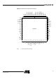
Block Diagram Figure 1.
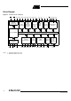
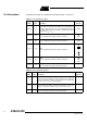
AT8xC5132 Pin Configuration P0.6/AD6 P0.7/AD7 P4.3/SS# P4.2/SCK P4.1/MOSI P4.0/MISO P2.0/A8 P2.1/A9 P4.7 P4.6 VSS VDD 80 79 78 77 76 75 74 73 72 71 70 69 68 67 66 65 64 63 62 61 P5.1 P5.0 P0.0/AD0 P0.1/AD1 P0.2/AD2 P0.3/AD3 P0.4/AD4 P0.5/AD5 Figure 2. AT8xC5132 80-pin TQFP Package ALE ISP# P1.0/KIN0 P1.1/KIN1 P1.2/KIN2 P1.3/KIN3 P1.4 P1.5 P1.6 P1.7 VDD PVDD FILT PVSS VSS TQFP80 60 59 58 57 56 55 54 53 52 51 50 49 48 47 46 45 44 43 42 41 P4.5 P4.4 P2.2/A10 P2.3/A11 P2.4/A12 P2.5/A13 P2.6/A14 P2.
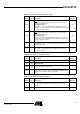
P2.1/A9 P2.0/A8 P4.0/MISO P4.1/MOSI P4.2/SCK P4.3/SS# P0.6/AD6 P0.7/AD7 VSS VDD P0.5/AD5 P0.4/AD4 P0.1 P0.2/AD2 P0.3/AD3 P0.0 Figure 3. AT8xC5132 64-pin TQFP 64 63 62 61 60 59 58 57 56 55 54 53 52 51 50 49 P1.0/KIN0 1 2 48 47 P1.1/KIN1 3 46 P1.2/KIN2 4 45 P1.3/KIN3 5 6 44 43 P2.4/A12 P2.5/A13 P2.6/A14 P2.7/A15 ISP# P1.4 P1.5 7 42 P1.6 8 9 41 40 P1.7 TQFP64 VDD 10 39 FILT 11 38 VSS X2 12 13 X1 14 36 35 TST# 15 16 33 UVDD 37 34 P4.5 P2.2/A10 P2.
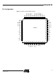
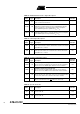
AT8xC5132 P0.6/AD6 P0.7/AD7 P4.3/SS# P4.2/SCK P4.1/MOSI P4.0/MISO P2.0/A8 P2.1/A9 P4.7 P4.6 VSS VDD 11 10 9 8 7 6 5 4 3 2 1 84 83 82 81 80 79 78 77 76 75 NC P5.1 P5.0 P0.0/AD0 P0.1/AD1 P0.2/AD2 P0.3/AD3 P0.4/AD4 P0.5/AD5 Figure 4. AT8xC5132 84-pin PLCC Package(1) ALE ISP# P1.0/KIN0 P1.1/KIN1 P1.2/KIN2 P1.3/KIN3 P1.4 P1.5 P1.6 P1.7 VDD PVDD FILT PVSS VSS PLCC84 74 73 72 71 70 69 68 67 66 65 64 63 62 61 60 59 58 57 56 55 54 NC P4.5 P4.4 P2.2/A10 P2.3/A11 P2.4/A12 P2.5/A13 P2.6/A14 P2.
Pin Description All AT8xC5132 signals are detailed by functionality in Table 1 to Table 14. Table 1. Ports Signal Description Signal Name Type Alternate Function Description P0.7:0 I/O Port 0 P0 is an 8-bit open-drain bidirectional I/O port. Port 0 pins that have 1s written to them float and can be used as high impedance inputs. To avoid any parasitic current consumption, floating P0 inputs must be polarized to VDD or VSS. P1.
AT8xC5132 Table 3. Timer 0 and Timer 1 Signal Description Signal Name Type Description Alternate Function Timer 0 Gate Input INT0 serves as external run control for timer 0, when selected by GATE0 bit in TCON register. INT0# I External Interrupt 0 INT0# input sets IE0 in the TCON register. If bit IT0 in this register is set, bit IE0 is set by a falling edge on INT0#. If bit IT0 is cleared, bit IE0 is set by a low level on INT0#. P3.
Table 6. MutiMediaCard Interface Signal Description Signal Name Type Alternate Function MCLK O MMC Clock output Data or command clock transfer. - MCMD I/O MMC Command line Bidirectional command channel used for card initialization and data transfer commands. To avoid any parasitic current consumption, unused MCMD input must be polarized to VDD or VSS. - MDAT I/O MMC Data line Bidirectional data channel.
AT8xC5132 Table 10. A/D Converter Signal Description Signal Name Type AIN1:0 I A/D Converter Analog Inputs - AREFP I Analog Positive Voltage Reference Input - AREFN I Analog Negative Voltage Reference Input This pin is internally connected to AVSS. - Description Alternate Function Table 11. Keypad Interface Signal Description Signal Name Type KIN3:0 I Description Keypad Input Lines Holding one of these pins high or low for 24 oscillator periods triggers a keypad interrupt.
Table 13. System Signal Description Signal Name Type Alternate Function Description RST I Reset Input Holding this pin high for 64 oscillator periods while the oscillator is running resets the device. The Port pins are driven to their reset conditions when a voltage lower than VIL is applied, whether or not the oscillator is running. This pin has an internal pull-down resistor which allows the device to be reset by connecting a capacitor between this pin and VDD.
AT8xC5132 Internal Pin Structure Table 15. Detailed Internal Pin Structure Circuit(1) Type Pins Input TST# Input/Output RST Input/Output P1 P2(3) P3 P4 P53:0 VDD P RRST Watchdog Output VSS 2 osc periods Latch Output VDD VDD VDD P1 P2 P3 N VSS VDD P Input/Output P0 MCMD MDAT ISP# N VSS VDD P Output N VSS D+ ALE SCLK DCLK DOUT DSEL MCLK Input/Output D+ D- D- Notes: 1.
Clock Controller The AT8xC5132 clock controller is based on an on-chip oscillator feeding an on-chip Phase Lock Loop (PLL). All internal clocks to the peripherals and CPU core are generated by this controller. Oscillator The AT8xC5132 X1 and X2 pins are the input and the output of a single-stage on-chip inverter (see Figure 5) that can be configured with off-chip components such as a Pierce oscillator (see Figure 6).
AT8xC5132 Figure 7. Mode Switching Waveforms X1 X1 ÷ 2 X2 bit Clock STD Mode Note: X2 Mode STD Mode In order to prevent any incorrect operation while operating in X2 mode, the user must be aware that all peripherals using clock frequency as time reference (timers…) will have their time reference divided by two. For example, a free running timer generating an interrupt every 20 ms will then generate an interrupt every 10 ms.
Figure 9. PLL Filter Connection PFILT R C2 C1 VSS PLL Programming VSS The PLL is programmed using the flow shown in Figure 10. As soon as clock generation is enabled, the user must wait until the lock indicator is set to ensure the clock output is stable. The PLL clock frequency will depend on the audio interface clock frequencies. Figure 10.
AT8xC5132 Registers Table 16. CKCON Register CKCON (S:8Fh) – Clock Control Register 7 6 5 4 3 2 1 0 - WDX2 - - - T1X2 T0X2 X2 Bit Number 7 Bit Mnemonic Description - Reserved The values read from this bit is indeterminate. Do not set this bit. Watchdog Clock Control Bit Set to select the oscillator clock divided by two as watchdog clock input (X2 independent). Clear to select the peripheral clock as watchdog clock input (X2 dependent).
Table 17. PLLCON Register PLLCON (S:E9h) – PLL Control Register 7 6 5 4 3 2 1 0 R1 R0 - - PLLRES - PLLEN PLOCK Bit Number Bit Mnemonic Description PLL Least Significant Bits R Divider 2 LSB of the 10-bit R divider. 7-6 R1:0 5-4 - 3 PLLRES 2 - 1 PLLEN PLL Enable Bit Set to enable the PLL. Clear to disable the PLL. 0 PLOCK PLL Lock Indicator Set by hardware when PLL is locked. Clear by hardware when PLL is unlocked. Reserved The values read from these Bits are always 0.
AT8xC5132 Table 19. PLLRDIV Register PLLRDIV (S:EFh) – PLL R Divider Register 7 6 5 4 3 2 1 0 R9 R8 R7 R6 R5 R4 R3 R2 Bit Number 7-0 Bit Mnemonic Description R9:2 PLL Most Significant Bits R Divider 8 MSB of the 10-bit R divider.
Program/Code Memory The AT89C5132 and AT83C5132 implement 64K Bytes of on-chip program/code memory. Figure 11 shows the split of internal and external program/code memory spaces depending on the product. The AT83C5132 product provides the internal program/code memory in ROM memory while the AT89C5132 product provides it in Flash memory. These two products do not allow external code memory execution. The Flash memory increases EPROM and ROM functionality by in-circuit electrical erasure and programming.
AT8xC5132 User Space This space is composed of a 64K Bytes ROM memory programmed during the manufacturing process. It contains the user’s application code. Flash Memory Architecture As shown in Figure 13 the AT89C5132 Flash memory is composed of four spaces detailed in the following paragraphs. Figure 13.
Extra Row Space This space is composed of two Bytes: Hardware Security System • The Software Boot Vector (SBV see Table 22). This byte is used by the software bootloader to build the boot address. • The Software Security Byte (SSB see Figure ). This byte is used to lock the execution of some bootloader commands.
AT8xC5132 Figure 14. Hardware Boot Process Algorithm RESET Software Process Hardware Process Hard Cond? ISP = L? Prog Cond? BLJB = P? Standard Init ENBOOT = 0 PC = 0000h FCON = F0h Prog Cond Init ENBOOT = 1 PC = F000h FCON = F0h User’s Application Atmel’s Boot Loader Hard Cond Init ENBOOT = 1 PC = F000h FCON = 00h The software process (bootloader) is detailed in the section “In-System and In-Application Programming”.
Registers Table 20. AUXR1 Register AUXR1 (S:A2h) – Auxiliary Register 1 7 6 5 4 3 2 1 0 - - ENBOOT - GF3 0 - DPS Bit Number 7-6 Bit Mnemonic Description - Reserved The values read from these Bits are indeterminate. Do not set these Bits. Enable Boot Flash Set this bit to map the boot Flash in the code space between at addresses F000h to FFFFh. Clear this bit to disable boot Flash.
AT8xC5132 Hardware Bytes Table 21. HSB Byte – Hardware Security Byte 7 6 5 4 3 2 1 0 X2B BLJB - - - LB2 LB1 LB0 Bit Number Bit Mnemonic Description X2 Bit Program this bit to start in X2 mode. Unprogram (erase) this bit to start in standard mode. 7 X2B(1)(2) 6 BLJB Boot Loader Jump Bit Program this bit to execute the bootloader at address F000h on next reset. Unprogram (erase) this bit to execute user’s application at address 0000h on next reset.
Data Memory The AT8xC5132 provides data memory access in two different spaces: 1. The internal space mapped in three separate segments: – The lower 128 Bytes RAM segment – The upper 128 Bytes RAM segment – The expanded 2048 Bytes RAM segment 2. The external space. A fourth internal segment is available but dedicated to Special Function Registers, SFRs, (addresses 80h to FFh) accessible by direct addressing mode.
AT8xC5132 Figure 16. Lower 128 Bytes Internal RAM Organization 7Fh 30h 2Fh 20h 18h 10h 08h 00h Bit-Addressable Space (Bit Addresses 0 - 7Fh) 1Fh 17h 0Fh 4 Banks of 8 Registers R0 - R7 07h Upper 128 Bytes RAM The upper 128 Bytes of RAM are accessible from address 80h to FFh using only indirect addressing mode. Expanded RAM The on-chip 2K Bytes of expanded RAM (ERAM) are accessible from address 0000h to 07FFh using indirect addressing mode through MOVX instructions.
External Space Memory Interface The external memory interface comprises the external bus (port 0 and port 2) as well as the bus control signals (RD, WR, and ALE). Figure 17 shows the structure of the external address bus. P0 carries address A7:0 while P2 carries address A15:8. Data D7:0 is multiplexed with A7:0 on P0. Table 26 describes the external memory interface signals. Figure 17.
AT8xC5132 External Bus Cycles This section describes the bus cycles that AT8xC5132 execute to read (see Figure 18), and write data (see Figure 19) in the external data memory. External memory cycle takes 6 CPU clock periods. This is equivalent to 12 oscillator clock periods in standard mode or 6 oscillator clock periods in X2 mode. For further information on X2 mode, refer to the section “X2 Feature”, page 12. Slow peripherals can be accessed by stretching the read and write cycles.
Dual Data Pointer Description The AT8xC5132 implement a second data pointer for speeding up code execution and reducing code size in case of intensive usage of external memory accesses. DPTR0 and DPTR1 are seen by the CPU as DPTR and are accessed using the SFR addresses 83h and 84h that are the DPH and DPL addresses. The DPS bit in AUXR1 register (see Table 29) is used to select whether DPTR is the data pointer 0 or the data pointer 1 (see Figure 20). Figure 20.
AT8xC5132 Registers Table 27. PSW Register PSW (S:8Eh) – Program Status Word Register 7 6 5 4 3 2 1 0 CY AC F0 RS1 RS0 OV F1 P Bit Number Bit Mnemonic Description 7 CY Carry Flag Carry out from bit 1 of ALU operands. 6 AC Auxiliary Carry Flag Carry out from bit 1 of addition operands. 5 F0 User Definable Flag 0. 4-3 RS1:0 Register Bank Select Bits Refer to Table 24 for Bits description. 2 OV Overflow Flag Overflow set by arithmetic operations.
Table 28. AUXR Register AUXR (S:8Eh) – Auxiliary Control Register 7 6 5 4 3 2 1 0 - EXT16 M0 DPHDIS XRS1 XRS0 EXTRAM AO Bit Number Bit Mnemonic Description Reserved The values read from this bit is indeterminate. Do not set this bit. 7 - 6 EXT16 5 M0 External Memory Access Stretch Bit Set to stretch RD or WR signals duration to 15 CPU clock periods. Clear not to stretch RD or WR signals and set duration to 3 CPU clock periods.
AT8xC5132 Special Function Registers The Special Function Registers (SFRs) of the AT8xC5132 derivatives fall into the categories detailed in Table 30 to Table 45. The relative addresses of these SFRs are provided together with their reset values in Table 46. In this table, the bit-addressable registers are identified by Note 1. Table 30.
Table 34. Port SFRs Mnemonic Add Name 7 6 5 4 3 2 1 0 P0 80h 8-bit Port 0 – – – – – – – – P1 90h 8-bit Port 1 – – – – – – – – P2 A0h 8-bit Port 2 – – – – – – – – P3 B0h 8-bit Port 3 – – – – – – – – P4 C0h 8-bit Port 4 – – – – – – – – P5 D8h 4-bit Port 5 – – – – – – – – 7 6 5 4 3 2 1 0 FPL3 FPL2 FPL1 FPL0 FPS FMOD1 FMOD0 FBUSY 7 6 5 4 3 2 1 0 Table 35.
AT8xC5132 Table 38.
Table 41. Serial I/O Port SFRs Mnemonic Add Name 7 6 5 4 3 2 1 0 FE/SM0 SM1 SM2 REN TB8 RB8 TI RI SCON 98h Serial Control SBUF 99h Serial Data Buffer – – – – – – – – SADEN B9h Slave Address Mask – – – – – – – – SADDR A9h Slave Address – – – – – – – – BDRCON 92h Baud Rate Control – – – BRR TBCK RBCK SPD SRC BRL 91h Baud Rate Reload – – – – – – – – 7 6 5 4 3 2 1 0 Table 42.
AT8xC5132 Table 46.
Interrupt System The AT8xC5132, like other control-oriented computer architectures, employ a program interrupt method. This operation branches to a subroutine and performs some service in response to the interrupt. When the subroutine terminates, execution resumes at the point where the interrupt occurred. Interrupts may occur as a result of internal AT8xC5132 activity (e.g., timer overflow) or at the initiation of electrical signals external to the microcontroller (e.g., keyboard).
AT8xC5132 Table 48. Priority Levels IPHxx IPLxx Priority Level 0 0 0 Lowest 0 1 1 1 0 2 1 1 3 Highest A low-priority interrupt is always interrupted by a higher priority interrupt but not by another interrupt of lower or equal priority. Higher priority interrupts are serviced before lower priority interrupts. The response to simultaneous occurrence of equal priority interrupts is determined by an internal hardware polling sequence detailed in Table 49.
Figure 21. Interrupt Control System INT0 00 01 10 11 External Interrupt 0 Highest Priority Interrupts EX0 00 01 10 11 IEN0.0 Timer 0 ET0 INT1 External Interrupt 1 00 01 10 11 IEN0.1 EX1 00 01 10 11 IEN0.2 Timer 1 ET1 TXD RXD Serial Port 00 01 10 11 IEN0.3 ES IEN0.4 00 01 10 11 Audio Interface EAUD MCLK MDAT MCMD MMC Controller 00 01 10 11 IEN0.6 EI2C SCK SI SO SPI Controller 00 01 10 11 IEN1.1 ESPI A-to-D Converter 00 01 10 11 IEN1.2 AIN1:0 EADC 00 01 10 11 IEN1.
AT8xC5132 External Interrupts INT1:0# Inputs External interrupts INT0 and INT1 (INTn, n = 0 or 1) pins may each be programmed to be level-triggered or edge-triggered, dependent upon Bits IT0 and IT1 (ITn, n = 0 or 1) in TCON register as shown in Figure 22. If ITn = 0, INTn is triggered by a low level at the pin. If ITn = 1, INTn is negative-edge triggered. External interrupts are enabled with Bits EX0 and EX1 (EXn, n = 0 or 1) in IEN0. Events on INTn set the interrupt request flag IEn in TCON register.
Registers Table 50. IEN0 Register IEN0 (S:A8h) – Interrupt Enable Register 0 7 6 5 4 3 2 1 0 EA EAUD – ES ET1 EX1 ET0 EX0 Bit Number 7 Bit Mnemonic Description EA Enable All Interrupt Bit Set to enable all interrupts. Clear to disable all interrupts. If EA = 1, each interrupt source is individually enabled or disabled by setting or clearing its interrupt enable bit. Audio Interface Interrupt Enable Bit Set to enable audio interface interrupt. Clear to disable audio interface interrupt.
AT8xC5132 Table 51. IEN1 Register IEN1 (S:B1h) – Interrupt Enable Register 1 7 6 5 4 3 2 1 0 - EUSB – EKB EADC ESPI EI2C EMMC Bit Number Bit Mnemonic Description Reserved The values read from this bit is always 0. Do not set this bit. 7 - 6 EUSB 5 – 4 EKB 3 EADC A-to-D Converter Interrupt Enable Bit Set to enable ADC interrupt. Clear to disable ADC interrupt. 2 ESPI SPI Controller Interrupt Enable Bit Set to enable SPI interrupt. Clear to disable SPI interrupt.
Table 52. IPH0 Register IPH0 (S:B7h) – Interrupt Priority High Register 0 7 6 5 4 3 2 1 0 - IPHAUD – IPHS IPHT1 IPHX1 IPHT0 IPHX0 Bit Number Bit Mnemonic Description Reserved The values read from this bit is indeterminate. Do not set this bit. 7 - 6 IPHAUD 5 – 4 IPHS Serial Port Interrupt Priority Level MSB Refer to Table 48 for priority level description. 3 IPHT1 Timer 1 Interrupt Priority Level MSB Refer to Table 48 for priority level description.
AT8xC5132 Table 53. IPH1 Register IPH1 (S:B3h) – Interrupt Priority High Register 1 7 6 5 4 3 2 1 0 - IPHUSB – IPHKB IPHADC IPHSPI IPHI2C IPHMMC Bit Number Bit Mnemonic Description Reserved The values read from this bit is always 0. Do not set this bit. 7 - 6 IPHUSB 5 - 4 IPHKB 3 IPHADC A-to-D Converter Interrupt Priority Level MSB Refer to Table 48 for priority level description. 2 IPHSPI SPI Interrupt Priority Level MSB Refer to Table 48 for priority level description.
Table 54. IPL0 Register IPL0 (S:B8h) – Interrupt Priority Low Register 0 7 6 5 4 3 2 1 0 - IPLAUD – IPLS IPLT1 IPLX1 IPLT0 IPLX0 Bit Number Bit Mnemonic Description Reserved The values read from this bit is indeterminate. Do not set this bit. 7 - 6 IPLAUD 5 – 4 IPLS Serial Port Interrupt Priority Level LSB Refer to Table 48 for priority level description. 3 IPLT1 Timer 1 Interrupt Priority Level LSB Refer to Table 48 for priority level description.
AT8xC5132 Table 55. IPL1 Register IPL1 (S:B2h) – Interrupt Priority Low Register 1 7 6 5 4 3 2 1 0 - IPLUSB - IPLKB IPLADC IPLSPI IPLI2C IPLMMC Bit Number Bit Mnemonic Description Reserved The values read from this bit is always 0. Do not set this bit. 7 - 6 IPLUSB 5 - 4 IPLKB 3 IPLADC A-to-D Converter Interrupt Priority Level LSB Refer to Table 48 for priority level description. 2 IPLSPI SPI Interrupt Priority Level LSB Refer to Table 48 for priority level description.
Power Management Two power reduction modes are implemented in the AT8xC5132: the Idle mode and the Power-down mode. In addition to these power reduction modes, the clocks of the core and peripherals can be dynamically divided by 2 using the X2 mode detailed in Section “X2 Feature”, page 12. Reset A reset is required after applying power at turn-on. To achieve a valid reset, the reset signal must be maintained for at least 2 machine cycles (24 oscillator clock periods) while the oscillator is running.
AT8xC5132 Idle Mode Idle mode is a power reduction mode that reduces the power consumption. In this mode, program execution halts. Idle mode freezes the clock to the CPU at known states while the peripherals continue to be clocked (refer to Section “Oscillator”, page 12). The CPU status before entering Idle mode is preserved, i.e., the program counter and program status word register retain their data for the duration of Idle mode. The contents of the SFRs and RAM are also retained.
Exiting Power-down Mode If VDD was reduced during the Power-down mode, do not exit Power-down mode until VDD is restored to the normal operating level. There are two ways to exit the Power-down mode: 1. Generate an enabled external interrupt. • The AT8xC5132 provides capability to exit from Power-down using INT0, INT1, and KIN3:0 inputs. In addition, using KIN input provides high or low level exit capability (see Section “Keyboard Interface”, page 134).
AT8xC5132 reset algorithm takes control. Reset initializes the AT8xC5132 and vectors the CPU to address 0000h. Notes: Registers 1. During the time that execution resumes, the internal RAM cannot be accessed; however, it is possible for the Port pins to be accessed. To avoid unexpected outputs at the Port pins, the instruction immediately following the instruction that activated the Power-down mode should not write to a Port pin or to the external RAM. 2.
Timers/Counters The AT8xC5132 implement two general-purpose, 16-bit Timers/Counters. They are identified as Timer 0 and Timer 1, and can be independently configured to operate in a variety of modes as a Timer or as an event Counter. When operating as a Timer, the Timer/Counter runs for a programmed length of time, then issues an interrupt request. When operating as a Counter, the Timer/Counter counts negative transitions on an external pin.
AT8xC5132 Figure 27. Timer 0 and Timer 1 Clock Controller and Symbols PER CLOCK 0 Timer 0 Clock PER CLOCK 0 Timer 1 Clock 1 OSC CLOCK 1 OSC CLOCK ÷2 T0X2 T1X2 CKCON.1 CKCON.2 TIM0 CLOCK TIM1 CLOCK Timer 0 Clock Symbol Timer 0 ÷2 Timer 1 Clock Symbol Timer 0 functions as either a Timer or event Counter in four modes of operation. Figure 28 through Figure 34 show the logical configuration of each mode.
Mode 1 (16-bit Timer) Mode 1 configures Timer 0 as a 16-bit Timer with TH0 and TL0 registers connected in cascade (see Figure 30). The selected input increments TL0 register. Figure 31 gives the overflow period calculation formula when in timer mode. Figure 30. Timer/Counter x (x = 0 or 1) in Mode 1 TIMx CLOCK ÷6 0 THx (8 Bits) 1 TLx (8 Bits) Overflow TFx TCON Reg Tx Timer x Interrupt Request C/Tx# TMOD Reg INTx# GATEx TRx TMOD Reg TCON Reg Figure 31.
AT8xC5132 Figure 34. Timer/Counter 0 in Mode 3: Two 8-bit Counters TIM0 CLOCK ÷6 0 1 TL0 (8 Bits) Overflow TH0 (8 Bits) Overflow TF0 TCON.5 T0 Timer 0 Interrupt Request C/T0# TMOD.2 INT0# GATE0 TR0 TMOD.3 TIM0 CLOCK TCON.4 ÷6 TF1 TCON.7 Timer 1 Interrupt Request TR1 TCON.6 Figure 35.
Mode 1 (16-bit Timer) Mode 1 configures Timer 1 as a 16-bit Timer with TH1 and TL1 registers connected in cascade (see Figure 30). The selected input increments TL1 register. Mode 2 (8-bit Timer with Auto-Reload) Mode 2 configures Timer 1 as an 8-bit Timer (TL1 register) with automatic reload from TH1 register on overflow (see Figure 32). TL1 overflow sets TF1 flag in TCON register and reloads TL1 with the contents of TH1, which is preset by software. The reload leaves TH1 unchanged.
AT8xC5132 Registers Table 58. TCON Register TCON (S:88h) – Timer/Counter Control Register 7 6 5 4 3 2 1 0 TF1 TR1 TF0 TR0 IE1 IT1 IE0 IT0 Bit Number Bit Mnemonic Description 7 TF1 Timer 1 Overflow Flag Cleared by hardware when processor vectors to interrupt routine. Set by hardware on Timer/Counter overflow, when Timer 1 register overflows. 6 TR1 Timer 1 Run Control Bit Clear to turn off Timer/Counter 1. Set to turn on Timer/Counter 1.
Table 59. TMOD Register TMOD (89:h) - Timer/Counter 0 and 1 Modes 7 6 5 4 3 2 1 0 GATE1 C/T1# M11 M01 GATE0 C/T0# M10 M00 Bit Bit Number Mnemonic Description 7 GATE1 Timer 1 Gating Control Bit Clear to enable Timer 1 whenever TR1 bit is set. Set to enable Timer 1 only while INT1 pin is high and TR1 bit is set. 6 C/T1# Timer 1 Counter/Timer Select Bit Clear for Timer operation: Timer 1 counts the divided-down system clock.
AT8xC5132 Table 61. TL0 Register TL0 (S:8Ah) – Timer 0 Low Byte Register 7 6 5 4 3 2 1 0 - - - - - - - - Bit Number Bit Mnemonic Description 7:0 Low Byte of Timer 0 Reset Value = 0000 0000b Table 62. TH1 Register TH1 (S:8Dh) – Timer 1 High Byte Register 7 6 5 4 3 2 1 0 - - - - - - - - Bit Number Bit Mnemonic Description 7:0 High Byte of Timer 1 Reset Value = 0000 0000b Table 63.
Watchdog Timer The AT8xC5132 implement a hardware Watchdog Timer (WDT) that automatically resets the chip if it is allowed to time out. The WDT provides a means of recovering from routines that do not complete successfully due to software or hardware malfunctions. Description The WDT consists of a 14-bit prescaler followed by a 7-bit programmable counter. As shown in Figure 37, the 14-bit prescaler is fed by the WDT clock detailed in section "Watchdog Clock Controller", page 58.
AT8xC5132 Watchdog Operation After reset, the WDT is disabled. The WDT is enabled by writing the sequence 1Eh and E1h into the WDTRST register. As soon as it is enabled, there is no way except the chip reset to disable it. If it is not cleared using the previous sequence, the WDT overflows and forces a chip reset. This overflow generates a high level 96 oscillator periods pulse on the RST pin to globally reset the application.
Registers Table 64. WDTRST Register WDTRST (S:A6h Write only) – Watchdog Timer Reset Register 7 6 5 4 3 2 1 0 - - - - - - - - Bit Number 7-0 Bit Mnemonic Description - Watchdog Control Value. Reset Value = XXXX XXXXb Table 65. WDTPRG Register WDTPRG (S:A7h) – Watchdog Timer Program Register 7 6 5 4 3 2 1 0 - - - - - WTO2 WTO1 WTO0 Bit Number Bit Mnemonic Description 7-3 - 2-0 WTO2:0 Reserved The values read from these Bits are indeterminate. Do not set these Bits.
AT8xC5132 Audio Output Interface The AT8xC5132 implement an audio output interface allowing the audio bitstream to be output in various formats. It is compatible with right and left justification PCM and I2S formats and thanks to the on-chip PLL (see Section “Clock Controller”, page 12) allows connection of almost all of the commercial audio DAC families available on the market.
Clock Generator The audio interface clock is generated by division of the PLL clock. The division factor is given by AUCD4:0 Bits in AUDCLK register. Figure 41 shows the audio interface clock generator and its calculation formula. The audio interface clock frequency depends on the audio DAC used. Figure 41.
AT8xC5132 Figure 43. Audio Output Format DSEL DCLK DOUT Left Channel 1 2 3 Right Channel 13 14 15 LSB MSB B14 16 B1 1 2 3 13 14 15 LSB MSB B14 16 B1 I2S Format with DSIZ = 0 and JUST4:0 = 00001. DSEL DCLK Left Channel 1 DOUT 2 Right Channel 3 17 MSB B14 LSB 18 32 1 2 3 17 MSB B14 LSB 18 32 I2S Format with DSIZ = 1 and JUST4:0 = 00001.
Table 66. Sample Duplication Factor Interrupt Request DUP1 DUP0 Factor 0 0 No sample duplication, DAC rate = 8 kHz (C51 rate). 0 1 One sample duplication, DAC rate = 16 kHz (2 x C51 rate). 1 0 Two samples duplication, DAC rate = 32 kHz (4 x C51 rate). 1 1 Three samples duplication, DAC rate = 48 kHz (6 x C51 rate).
AT8xC5132 Figure 45. Voice or Sound Mode Audio Flows Voice/Song Mode Configuration Program Audio Clock Configure Interface HLR = X DSIZ = X POL = X JUST4:0 = XXXXXb DUP1:0 = XX Enable DAC System Clock AUDEN = 1 Note: Audio Interrupt Service Routine Wait for DAC Enable Time Sample Request? SREQ = 1? Select Audio SRC = 1 Load 4 Samples in the Audio Buffer Under-run Condition1 Load 8 Samples in the Audio Buffer Enable Interrupt Set MSREQ & MUDRN1 EAUD = 1 1.
Registers Table 67. AUDCON0 Register AUDCON0 (S:9Ah) – Audio Interface Control Register 0 7 6 5 4 3 2 1 0 JUST4 JUST3 JUST2 JUST1 JUST0 POL DSIZ HLR Bit Number Bit Mnemonic Description Audio Stream Justification Bits Refer to Section "Data Converter", page 62 for Bits description. 7-3 JUST4:0 2 POL DSEL Signal Output Polarity Set to output the left channel on high level of DSEL output (PCM mode). Clear to output the left channel on the low level of DSEL output (I2S mode).
AT8xC5132 Table 69. AUDSTA Register AUDSTA (S:9Ch Read Only) – Audio Interface Status Register 7 6 5 4 3 2 1 0 SREQ UDRN AUBUSY - - - - - Bit Number Bit Mnemonic Description SREQ Audio Sample Request Flag Set in C51 audio source mode when the audio interface request samples (buffer half empty). This bit generates an interrupt if not masked and if enabled in IEN0. Cleared by hardware when samples are loaded in AUDDAT.
Universal Serial Bus The AT8xC5132 implement a USB device controller supporting Full-speed data transfer. In addition to the default control endpoint 0, it provides 3 other endpoints, which can be configured in Control, Bulk, Interrupt or Isochronous types. This allows to develop firmware conforming to most USB device classes, for example the AT8xC5132 support: USB Mass Storage Class CBI Transport • USB Mass Storage Class Control/Bulk/Interrupt (CBI) Transport, Revision 1.
AT8xC5132 Description The USB device controller provides the hardware that the AT8xC5132 need to interface a USB link to data flow stored in a double port memory. It requires a 48 MHz reference clock provided by the clock controller as detailed in Section "Clock Controller", page 69. This clock is used to generate a 12 MHz full speed bit clock from the received USB differential data flow and to transmit data according to full speed USB device tolerance.
Serial Interface Engine (SIE) The SIE performs the following functions: • NRZI data encoding and decoding • Bit stuffing and unstuffing • CRC generation and checking • ACKs and NACKs automatic generation • TOKEN type identifying • Address checking • Clock recovery (using DPLL) Figure 48.
AT8xC5132 Figure 49. UFI Block Diagram Transfer Control FSM 12 MHz DPLL Asynchronous Information USBCON USBADDR USBINT USBIEN UEPNUM UEPCONX UEPSTAX UEPRST UEPINT UEPIEN UEPDATX UBYCTX UFNUMH UFNUML To/From C51 Core Endpoint 3 Endpoint 2 Endpoint Control USB side To/From SIE Endpoint Control C51 side Endpoint 1 Endpoint 0 Figure 50.
Endpoint Interrupt Sources Each endpoint supports four interrupt sources reported in UEPSTAX and combined together to appear as a single endpoint interrupt source in UEPINT. Each endpoint interrupt can be enabled separately in UEPIEN. • TXCMP: Transmitted In Data Interrupt Flag. This flag triggers an interrupt after an IN packet has been transmitted for Isochronous endpoints or after it has been accepted (ACK’ed) by the host for Control, Bulk and Interrupt endpoints.
AT8xC5132 Registers Table 72. USBCON Register USBCON (S:BCh) – USB Global Control Register 7 6 5 4 3 2 1 0 USBE SUSPCLK SDRMWUP - UPRSM RMWUPE CONFG FADDEN Bit Number Bit Mnemonic Description 7 USBE 6 SUSPCLK 5 Suspend USB Clock Bit Set to disable the 48 MHz clock input (Resume Detection is still active). Clear to enable the 48 MHz clock input. Send Remote Wake-up Bit Set to force an external interrupt on the USB controller for Remote Wake UP purpose.
Table 73. USBADDR Register USBADDR (S:C6h) – USB Address Register 7 6 5 4 3 2 1 0 FEN UADD6 UADD5 UADD4 UADD3 UADD2 UADD1 UADD0 Bit Number Bit Mnemonic Description 7 6-0 Function Enable Bit Set to enable the function. The device firmware shall set this bit after it has received a USB reset and participate in the following configuration process with the default address (FEN is reset to 0). Cleared by hardware at power-up, should not be cleared by the device firmware once set.
AT8xC5132 Table 75. USBIEN Register USBIEN (S:BEh) – USB Global Interrupt Enable Register 7 6 5 4 3 2 1 0 - - EWUPCPU EEORINT ESOFINT - - ESPINT Bit Number Bit Mnemonic Description 7-6 - 5 Reserved The values read from these Bits are always 0. Do not set these Bits. Wake up CPU Interrupt Enable Bit EWUPCPU Set to enable the Wake Up CPU interrupt. Clear to disable the Wake Up CPU interrupt. 4 EEOFINT End Of Reset Interrupt Enable Bit Set to enable the End Of Reset interrupt.
Table 77. UEPCONX Register UEPCONX (S:D4h) – USB Endpoint X Control Register (X = EPNUM set in UEPNUM) 7 6 5 4 3 2 1 0 EPEN - - - DTGL EPDIR EPTYPE1 EPTYPE0 Bit Number Bit Mnemonic Description 7 EPEN 6-4 - Endpoint Enable Bit Set to enable the endpoint according to the device configuration. Endpoint 0 shall always be enabled after a hardware or USB bus reset and participate in the device configuration. Clear to disable the endpoint according to the device configuration.
AT8xC5132 Table 78. UEPSTAX Register UEPSTAX (Soh) – USB Endpoint X Status and Control Register (X = EPNUM set in UEPNUM) 7 6 5 4 3 2 1 0 DIR - STALLRQ TXRDY STLCRC RXSETUP RXOUT TXCMP Bit Number Bit Mnemonic Description Control Endpoint Direction Bit This bit is relevant only if the endpoint is configured in Control type. Set for the data stage. Clear otherwise. 7 DIR 6 - 5 STALLRQ Stall Handshake Request Bit Set to send a STALL answer to the host for the next handshake.
Table 79. UEPRST Register UEPRST (S:D5h) – USB Endpoint FIFO Reset Register 7 6 5 4 3 2 1 0 - - - - EP3RST EP2RST EP1RST EP0RST Bit Number Bit Mnemonic Description Reserved The values read from these Bits are always 0. Do not set these Bits. 7-4 - 3 EP3RST Endpoint 3 FIFO Reset Set and clear to reset the endpoint 3 FIFO prior to any other operation, upon hardware reset or when an USB bus reset has been received.
AT8xC5132 Table 81. UEPIEN Register UEPIEN (S:C2h) – USB Endpoint Interrupt Enable Register 7 6 5 4 3 2 1 0 - - - - EP3INTE EP2INTE EP1INTE EP0INTE Bit Number Bit Mnemonic Description Reserved The values read from these Bits are always 0. Do not set these Bits. 7-4 - 3 EP3INTE Endpoint 3 Interrupt Enable Bit Set to enable the interrupts for endpoint 3. Clear to disable the interrupts for endpoint 3.
Table 83. UBYCTLX Register UBYCTX (S:E2h) – USB Endpoint X Byte Count Register (X = EPNUM set in UEPNUM) 7 6 5 4 3 2 1 0 - BYCT6 BYCT5 BYCT4 BYCT3 BYCT2 BYCT1 BYCT0 Bit Number Bit Mnemonic Description 7 - 6-0 BYCT7:0 Reserved The values read from this Bits are always 0. Do not set this bit. Byte Count Byte count of a received data packet. This byte count is equal to the number of data Bytes received after the Data PID. Reset Value = 0000 0000b Table 84.
AT8xC5132 Table 85. UFNUMH Register UFNUMH (S:BBh, Read-only) – USB Frame Number High Register 7 6 5 4 3 2 1 0 - - CRCOK CRCERR - FNUM10 FNUM9 FNUM8 Bit Number Bit Mnemonic 7-3 - 5 Description Reserved The values read from these Bits are always 0. Do not set these Bits. CRCOK Frame Number CRC OK Bit Set by hardware after a non corrupted Frame Number in Start of Frame Packet is received. Updated after every Start Of Frame packet reception.
MultiMedia Card Controller The AT8xC5132 implements a MultiMedia Card (MMC) controller. The MMC is used to store files in removable Flash memory cards that can be easily plugged or removed from the application. Card Concept The basic MultiMedia Card concept is based on transferring data via a minimal number of signals. Card Signals The communication signals are: Card Registers • CLK: with each cycle of this signal an one bit transfer on the command and data lines is done.
AT8xC5132 Bus Lines The MultiMedia Card bus architecture requires all cards to be connected to the same set of lines. No card has an individual connection to the host or other devices, which reduces the connection costs of the MultiMedia Card system. The bus lines can be divided into three groups: Bus Protocol • Power supply: VSS1 and VSS2, VDD – used to supply the cards. • Data transfer: MCMD, MDAT – used for bidirectional communication.
Figure 53. (Multiple) Block Read Operation Stop Command MCMD Command Response MDAT Command Response Data Block CRC Data Block CRC Data Block CRC Block Read Operation Data Stop Operation Multiple Block Read Operation As shown in Figure 54 and Figure 55 the data write operation uses a simple busy signalling of the write operation duration on the data line (MDAT). Figure 54.
AT8xC5132 Table 87. Command Token Format Bit Position 47 46 45:40 39:8 7:1 0 Width (Bits) 1 1 6 32 7 1 Value ‘0’ ‘1’ - - - ‘1’ Start bit Transmission bit Command Index Argument CRC7 End bit Description Response Token Format There are five types of response tokens (R1 to R5). As shown in Figure 58, responses have a code length of 48 Bits or 136 Bits. A response token is preceded by a Start bit: a low level on MCMD line and succeeded by an End bit: a high level on MCMD line.
Table 90. R3 Response Format (OCR Register) Bit Position 47 46 [45:40] [39:8] [7:1] 0 Width (Bits) 1 1 6 32 7 1 Value ‘0’ ‘0’ ‘111111’ - ‘1111111’ ‘1’ Start bit Transmission bit Reserved OCR register Reserved End bit Description Table 91. R4 Response Format (Fast I/O) Bit Position 47 46 [45:40] [39:8] [7:1] 0 Width (Bits) 1 1 6 32 7 1 Value ‘0’ ‘0’ ‘100111’ - - ‘1’ Start bit Transmission bit Command Index Argument CRC7 End bit Description Table 92.
AT8xC5132 Clock Control The MMC bus clock signal can be used by the host to turn the cards into energy saving mode or to control the data flow (to avoid under-run or over-run conditions) on the bus. The host is allowed to lower the clock frequency or shut it down.
Clock Generator The MMC clock is generated by division of the oscillator clock (FOSC) issued from the Clock Controller block as detailed in Section "Oscillator", page 12. The division factor is given by MMCD7:0 Bits in MMCLK register. Figure 61 shows the MMC clock generator and its output clock calculation formula. Figure 61. MMC Clock Generator and Symbol OSC CLOCK Controller Clock OSCclk MMCclk = ----------------------------MMCD + 1 MMCLK MMCEN MMCON2.
AT8xC5132 Command Line Controller As shown in Figure 63, the command line controller is divided in two channels: the command transmitter channel that handles the command transmission to the card through the MCMD line and the command receiver channel that handles the response reception from the card through the MCMD line. These channels are detailed in the following sections. Figure 63. Command Line Controller Block Diagram TX Pointer CTPTR MMCON0.
The user may abort command loading by setting and clearing the CTPTR bit in MMCON0 register which resets the write pointer to the transmit FIFO. Figure 64. Command Transmission Flow Command Transmission Configure Response RESPEN = X RFMT = X CRCDIS = X Load Command in Buffer MMCMD = Index MMCMD = Argument Transmit Command CMDEN = 1 CMDEN = 0 Command Receiver The end of the response reception is signalled by the EORI flag in MMINT register.
AT8xC5132 Data Line Controller The data line controller is based on a 16-byte FIFO used both by the data transmitter channel and by the data receiver channel. Figure 65. Data Line Controller Block Diagram MMINT.0 MMINT.2 MMSTA.3 MMSTA.4 F1EI F1FI DATFS CRC16S CRC16 and Format Checker Data Converter Serial -> // 8-byte TX Pointer FIFO 1 DTPTR MMCON0.6 RX Pointer DRPTR MMCON0.7 FIFO Implementation 16-byte FIFO MMDAT MCBI CBUSY MMINT.1 MMSTA.
Figure 66. Data Controller Configuration Flows Data Stream Configuration Data Single Block Configuration Data Multi-block Configuration Configure Format DFMT = 0 Configure Format DFMT = 1 MBLOCK = 0 BLEN3:0 = XXXXb Configure Format DFMT = 1 MBLOCK = 1 BLEN3:0 = XXXXb Data Transmitter Configuration For transmitting data to the card, user must first configure the data controller in transmission mode by setting the DATDIR bit in MMCON1 register.
AT8xC5132 Figure 67.
Figure 68.
AT8xC5132 This time-out may be disarmed after receiving 8 data (F1FI flag set) or after receiving end of frame (EOFI flag set) in case of block length less than 8 data (1, 2 or 4). Data Reading Data is read from the FIFO by reading to MMDAT register. Each time one FIFO becomes full (F1FI or F2FI set), user is requested to flush this FIFO by reading 8 data. Figure 69.
Figure 70. Data Block Reception Flows Data Block Reception Data Block Initialization Data Block Reception ISR Start Transmission DATEN = 1 DATEN = 0 Unmask FIFOs Full F1FM = 0 F2FM = 0 FIFO Full? F1EI or F2EI = 1? FIFO Full? F1EI or F2EI = 1? Start Transmission DATEN = 1 DATEN = 0 FIFO Reading read 8 data from MMDAT FIFO Reading read 8 data from MMDAT No More Data To Receive? No More Data To Receive? Mask FIFOs Full F1FM = 1 F2FM = 1 a. Polling Mode b.
AT8xC5132 Interrupt Description As shown in Figure 71, the MMC controller implements eight interrupt sources reported in MCBI, EORI, EOCI, EOFI, F2FI, F1FI, and F2EI flags in MMCINT register. These flags were detailed in the previous sections. All of these sources are maskable separately using MCBM, EORM, EOCM, EOFM, F2FM, F1FM, and F2EM mask bits, respectively, in MMMSK register.
Registers Table 94. MMCON0 Register MMCON0 (S:E4h) – MMC Control Register 0 7 6 5 4 3 2 1 0 DRPTR DTPTR CRPTR CTPTR MBLOCK DFMT RFMT CRCDIS Bit Number Bit Mnemonic Description 7 DRPTR Data Receive Pointer Reset Bit Set to reset the read pointer of the data FIFO. Clear to release the read pointer of the data FIFO. 6 DTPTR Data Transmit Pointer Reset Bit Set to reset the write pointer of the data FIFO. Clear to release the write pointer of the data FIFO.
AT8xC5132 Table 95. MMCON1 Register MMCON1 (S:E5h) – MMC Control Register 1 7 6 5 4 3 2 1 0 BLEN3 BLEN2 BLEN1 BLEN0 DATDIR DATEN RESPEN CMDEN Bit Number Bit Mnemonic Description 7-4 BLEN3:0 Block Length Bits Refer to Table 93 for Bits description. Do not program value > 1011b. 3 DATDIR Data Direction Bit Set to select data transfer from host to card (write mode). Clear to select data transfer from card to host (read mode).
Table 97. MMSTA Register MMSTA (S:DEh Read Only) – MMC Control and Status Register 7 6 5 4 3 2 1 0 - - CBUSY CRC16S DATFS CRC7S RESPFS CFLCK Bit Number Bit Mnemonic Description Reserved The values read from these Bits are always 0. Do not set these Bits. 7-6 - 5 CBUSY Card Busy Flag Set by hardware when the card sends a busy state on the data line. Cleared by hardware when the card no more sends a busy state on the data line.
AT8xC5132 Table 98. MMINT Register MMINT (S:E7h Read Only) – MMC Interrupt Register 7 6 5 4 3 2 1 0 MCBI EORI EOCI EOFI F2FI F1FI F2EI F1EI Bit Number Bit Mnemonic Description 7 MCBI MMC Card Busy Interrupt Flag Set by hardware when the card enters or exits its busy state (when the busy signal is asserted or deasserted on the data line). Cleared when reading MMINT. 6 EORI End of Response Interrupt Flag Set by hardware at the end of response reception. Cleared when reading MMINT.
Table 99. MMMSK Register MMMSK (S:DFh) – MMC Interrupt Mask Register 7 6 5 4 3 2 1 0 MCBM EORM EOCM EOFM F2FM F1FM F2EM F1EM Bit Number Bit Mnemonic Description 7 MCBM MMC Card Busy Interrupt Mask Bit Set to prevent MCBI flag from generating an MMC interrupt. Clear to allow MCBI flag to generate an MMC interrupt. 6 EORM End Of Response Interrupt Mask Bit Set to prevent EORI flag from generating an MMC interrupt. Clear to allow EORI flag to generate an MMC interrupt.
AT8xC5132 Table 101. MMDAT Register MMDAT (S:DCh) – MMC Data Register 7 6 5 4 3 2 1 0 MD7 MD6 MD5 MD4 MD3 MD2 MD1 MD0 Bit Number 7-0 Bit Mnemonic Description MD7:0 MMC Data Byte Input (write) or output (read) register of the data FIFO. Reset Value = 1111 1111b Table 102.
IDE/ATAPI Interface The AT8xC5132 provide an IDE/ATAPI interface allowing connection of devices such as CD-ROM reader, CompactFlash cards, hard disk drive, etc. It consists of a 16-bit data transfer (read or write) between the AT8xC5132 and the IDE devices. Description The IDE interface mode is enabled by setting the EXT16 bit in AUXR (see Table 28 on page 30). As soon as this bit is set, all MOVX instructions read or write are done in a 16bit mode compare to the standard 8-bit mode.
AT8xC5132 Figure 73. IDE Write Waveforms CPU Clock ALE WR(1) P0 P2 Notes: IDE Device Connection P2 DPL or Ri D7:0 DPH or P2(2),(3) D15:8 P2 1. WR signal may be stretched using M0 bit in AUXR register. 2. When executing MOVX @Ri instruction, P2 outputs SFR content. 3. When executing MOVX @DPTR instruction, if DPHDIS is set (Page Access Mode), P2 outputs SFR content instead of DPH. Figure 74 and Figure 75 show two examples on how to interface up to two IDE devices to the AT8xC5132.
Table 103. External Data Memory Interface Signals Registers Signal Name Type Alternate Function A15:8 I/O Address Lines Upper address lines for the external bus. Multiplexed higher address and data lines for the IDE interface. P2.7:0 AD7:0 I/O Address/Data Lines Multiplexed lower address and data lines for the IDE interface. P0.7:0 ALE O Address Latch Enable ALE signals indicates that valid address information is available on lines AD7:0.
AT8xC5132 Serial I/O Port The serial I/O port in the AT8xC5132 provides both synchronous and asynchronous communication modes. It operates as a Synchronous Receiver and Transmitter in one single mode (Mode 0) and operates as an Universal Asynchronous Receiver and Transmitter (UART) in three full-duplex modes (modes 1, 2 and 3). Asynchronous modes support framing error detection and multiprocessor communication with automatic address recognition.
Internal Baud Rate Generator When using the Internal Baud Rate Generator, the Baud Rate is derived from the overflow of the timer. As shown in Figure 77, the Internal Baud Rate Generator is an 8-bit auto-reload timer feed by the peripheral clock or by the peripheral clock divided by 6 depending on the SPD bit in BDRCON register (see Table 111). The Internal Baud Rate Generator is enabled by setting BBR bit in BDRCON register. SMOD1 bit in PCON register allows doubling of the generated baud rate.
AT8xC5132 Figure 79. Transmission Waveforms (Mode 0) TXD Write to SBUF RXD D0 D1 D2 D3 D4 D5 D6 D7 TI Reception (Mode 0) To start a reception in mode 0, write to SCON register clearing SM0, SM1 and RI Bits and setting the REN bit. As shown in Figure 80, Clock is pulsed and the LSB (D0) is sampled on the RXD pin. The D0 bit is then shifted into the shift register. After eight sampling, the MSB (D7) is shifted into the shift register, and hardware asserts RI bit to indicate a completed reception.
Asynchronous Modes (Modes 1, 2 and 3) The Serial Port has one 8-bit and two 9-bit asynchronous modes of operation. Figure 83 shows the Serial Port block diagram in asynchronous modes. Figure 83. Serial I/O Port Block Diagram (Modes 1, 2 and 3) SCON.6 SCON.7 SCON.3 SM1 SM0 TB8 Mode Decoder SBUF Tx SR TXD Rx SR RXD M3 M2 M1 M0 T1 CLOCK Mode & Clock Controller IBRG CLOCK SBUF Rx PER CLOCK RB8 SCON.2 SM2 TI RI SCON.4 SCON.1 SCON.0 Mode 1 Mode 1 is a full-duplex, asynchronous mode.
AT8xC5132 Framing Error Detection (Modes 1, 2 and 3) Framing error detection is provided for the three asynchronous modes. To enable the framing bit error detection feature, set SMOD0 bit in PCON register as shown in Figure 86. When this feature is enabled, the receiver checks each incoming data frame for a valid stop bit. An invalid stop bit may result from noise on the serial lines or from simultaneous transmission by two devices.
Table 106. Baud Rate Generator Configuration FPER = 6 MHz(1) FPER = 8 MHz(1) FPER = 10 MHz(1) Baud Rate SPD SMOD1 BRL Error% SPD SMOD1 BRL Error% SPD SMOD1 BRL Error% 115200 - - - - - - - - - - - - 57600 - - - - 1 1 247 3.55 1 1 245 1.36 38400 1 1 246 2.34 1 1 243 0.16 1 1 240 1.73 19200 1 1 236 2.34 1 1 230 0.16 1 1 223 1.36 9600 1 1 217 0.16 1 1 204 0.16 1 1 191 0.16 4800 1 1 178 0.16 1 1 152 0.16 1 1 126 0.
AT8xC5132 Multiprocessor Communication (Modes 2 and 3) Modes 2 and 3 provide a ninth-bit mode to facilitate multiprocessor communication. To enable this feature, set SM2 bit in SCON register. When the multiprocessor communication feature is enabled, the Serial Port can differentiate between data frames (ninth bit clear) and address frames (ninth bit set). This allows the AT8xC5132 to function as a slave processor in an environment where multiple slave processors share a single serial line.
The SADEN byte is selected so that each slave may be addressed separately. For slave A, bit 0 (the LSB) is a don’t care bit; for slaves B and C, bit 0 is a 1. To communicate with slave A only, the master must send an address where bit 0 is clear (e.g. 1111 0000B). For slave A, bit 1 is a 0; for slaves B and C, bit 1 is a don’t care bit. To communicate with slaves A and B, but not slave C, the master must send an address with Bits 0 and 1 both set (e.g. 1111 0011B).
AT8xC5132 Interrupt The Serial I/O Port handles two interrupt sources that are the “end of reception” (RI in SCON) and “end of transmission” (TI in SCON) flags. As shown in Figure 91 these flags are combined together to appear as a single interrupt source for the C51 core. Flags must be cleared by software when executing the serial interrupt service routine. The serial interrupt is enabled by setting ES bit in IEN0 register. This assumes interrupts are globally enabled by setting EA bit in IEN0 register.
Registers Table 107. SCON Register SCON (S:98h) – Serial Control Register 7 6 5 4 3 2 1 0 FE/SM0 OVR/SM1 SM2 REN TB8 RB8 TI RI Bit Number Bit Mnemonic Description FE 7 Framing Error Bit To select this function, set SMOD0 bit in PCON register. Set by hardware to indicate an invalid stop bit. Must be cleared by software. SM0 Serial Port Mode Bit 0 Refer to Table 105 for mode selection. SM1 Serial Port Mode Bit 1 Refer to Table 105 for mode selection.
AT8xC5132 Table 108. SBUF Register SBUF (S:99h) – Serial Buffer Register 7 6 5 4 3 2 1 0 SD7 SD6 SD5 SD4 SD3 SD2 SD1 SD0 Bit Number 7-0 Bit Mnemonic Description SD7:0 Serial Data Byte Read the last data received by the Serial I/O Port. Write the data to be transmitted by the Serial I/O Port. Reset value = XXXX XXXXb Table 109.
Table 111. BDRCON Register BDRCON (S:92h) – Baud Rate Generator Control Register 7 6 5 4 3 2 1 0 - - - BRR TBCK RBCK SPD M0SRC Bit Number Bit Mnemonic Description Reserved The values read from these Bits are indeterminate. Do not set these Bits. 7-5 - 4 BRR Baud Rate Run Bit Set to enable the baud rate generator. Clear to disable the baud rate generator. 3 TBCK Transmission Baud Rate Selection Bit Set to select the baud rate generator as transmission baud rate generator.
AT8xC5132 Synchronous Peripheral Interface The AT8xC5132 implement a Synchronous Peripheral Interface with master and slave modes capability. Figure 93 shows an SPI bus configuration using the AT8xC5132 as master connected to slave peripherals. Figure 94 shows an SPI bus configuration using the AT8xC5132 as slave of an other master. The bus is made of three wires connecting all the devices together: • Master Output Slave Input (MOSI): it is used to transfer data in series from the master to a slave.
Description The SPI controller interfaces with the C51 core through three special function registers: SPCON, the SPI control register (see Table 114); SPSTA, the SPI status register (see Table 115); and SPDAT, the SPI data register (see Table 116). Master Mode The SPI operates in master mode when the MSTR bit in SPCON is set. Figure 95 shows the SPI block diagram in master mode. Only a master SPI module can initiate transmissions. Software begins the transmission by writing to SPDAT.
AT8xC5132 Figure 96. SPI Slave Mode Block Diagram MISO/P4.2 I 8-bit Shift Register Q Internal Bus MOSI/P4.1 SPDAT WR SPDAT RD SCK/P4.2 Control and Clock Logic SS/P4.3 SPIF SPSTA.7 SSDIS SPCON.5 Note: CPHA CPOL SPCON.2 SPCON.3 MSTR bit in SPCON is cleared to select slave mode. Bit Rate The bit rate can be selected from seven predefined bit rates using the SPR2, SPR1 and SPR0 control Bits in SPCON according to Table 113.
Figure 97. Data Transmission Format (CPHA = 0) SCK Cycle Number 1 2 3 4 5 6 7 8 MSB bit 6 bit 5 bit 4 bit 3 bit 2 bit 1 LSB bit 6 bit 5 bit 4 bit 3 bit 2 bit 1 LSB SPEN (Internal) SCK (CPOL = 0) SCK (CPOL = 1) MOSI (from Master) MISO (from Slave) MSB SS (to Slave) to Capture Point Figure 98.
AT8xC5132 Figure 99. SS# Timing Diagram SI/SO Byte 1 Byte 2 Byte 3 SS (CPHA = 0) SS (CPHA = 1) Error Conditions Interrupt The following flags signal the SPI error conditions: • MODF in SPSTA signals a mode fault. MODF flag is relevant only in master mode when SS usage is enabled (SSDIS bit cleared). It signals when set that another master on the bus has asserted SS pin and so, may create a conflict on the bus with two masters sending data at the same time.
Configuration The SPI configuration is made through SPCON. Master Configuration The SPI operates in master mode when the MSTR bit in SPCON is set. Slave Configuration The SPI operates in slave mode when the MSTR bit in SPCON is cleared and data has been loaded in SPDAT.
AT8xC5132 Master Mode with Interrupt Policy Figure 102 shows the initialization phase and the transfer phase flows using the interrupt policy. Using this flow prevents any overrun error occurrence. • The bit rate is selected according to Table 113. • The transfer format depends on the slave peripheral. • SS may be deasserted between transfers depending also on the slave peripheral. Reading SPSTA at the beginning of the ISR is mandatory for clearing the SPIF flag.
Slave Mode with Polling Policy Figure 103 shows the initialization phase and the transfer phase flows using the polling policy. The transfer format depends on the master controller. SPIF flag is cleared when reading SPDAT (SPSTA has been read before by the “end of reception” check). This policy provides the fastest effective transmission and is well adapted when communicating at high speed with other Microcontrollers. However, the procedure may be interrupted at any time by higher priority tasks.
AT8xC5132 Slave Mode with Interrupt Policy Figure 102 shows the initialization phase and the transfer phase flows using the interrupt policy. The transfer format depends on the master controller. Reading SPSTA at the beginning of the ISR is mandatory for clearing the SPIF flag. Clear is effective when reading SPDAT. Figure 104.
Bit Number Bit Mnemonic Description SPI Clock Polarity Bit(1) 3 CPOL 2 CPHA 1-0 SPR1:0 Set to have the clock output set to high level in idle state. Clear to have the clock output set to low level in idle state. SPI Clock Phase Bit Set to have the data sampled when the clock returns to idle state (see CPOL). Clear to have the data sampled when the clock leaves the idle state (see CPOL). SPI Rate Bits 0 and 1 Refer to Table 113 for bit rate description. Reset Value = 0001 0100b Note: 1.
AT8xC5132 Analog-to-Digital Converter The AT8xC5132 implement a 2-channel 10-bit (8 true Bits) analog-to-digital converter (ADC). The first channel of this ADC can be used for battery monitoring while the second channel can be used for voice sampling at 8 kHz.
Clock Generation The ADC clock is generated by division of the peripheral clock (see details in Section “X2 Feature”, page 12). The division factor is then given by ADCP4:0 Bits in ADCLK register. Figure 107 shows the ADC clock generator and its calculation formula(1). Figure 107.
AT8xC5132 Figure 108. ADC Configuration Flow ADC Configuration Program ADC Clock ADCD4:0 = xxxxxb Enable ADC ADIDL = x ADEN = 1 Wait Setup Time Conversion Launching The conversion is launched by setting the ADSST bit in ADCON register, this bit remains set during the conversion. As soon as the conversion is started, it takes 11 clock periods (TCONV) before the data is available in ADDH and ADDL registers. Figure 109.
Registers Table 118. ADCON Register ADCON (S:F3h) – ADC Control Register 7 6 5 4 3 2 1 0 - ADIDL ADEN ADEOC ADSST - - ADCS Bit Number Bit Mnemonic Description Reserved The values read from this bit is always 0. Do not set this bit. 7 - 6 ADIDL ADC Pseudo-Idle Mode Set to suspend the CPU core activity (pseudo-idle mode) during conversion. Clear by hardware at the end of conversion. 5 ADEN ADC Enable Bit Set to enable the A-to-D converter.
AT8xC5132 Table 120. ADDH Register ADDH (S:F5h Read Only) – ADC Data High Byte Register 7 6 5 4 3 2 1 0 ADAT9 ADAT8 ADAT7 ADAT6 ADAT5 ADAT4 ADAT3 ADAT2 Bit Number 7-0 Bit Mnemonic Description ADAT9:2 ADC Data Eight Most Significant Bits of the 10-bit ADC data. Reset Value = 0000 0000b Table 121.
Keyboard Interface The AT8xC5132 implement a keyboard interface allowing the connection of a 4 x n matrix keyboard. It is based on 4 inputs with programmable interrupt capability on both high or low level. These inputs are available as alternate function of P1.3:0 and allow exit from idle and power down modes.
AT8xC5132 Registers Table 122. KBCON Register KBCON (S:A3h) – Keyboard Control Register 7 6 5 4 3 2 1 0 KINL3 KINL2 KINL1 KINL0 KINM3 KINM2 KINM1 KINM0 Bit Number Bit Mnemonic Description 7-4 KINL3:0 Keyboard Input Level Bit Set to enable a high level detection on the respective KIN3:0 input. Clear to enable a low level detection on the respective KIN3:0 input. 3-0 KINM3:0 Keyboard Input Mask Bit Set to prevent the respective KINF3:0 flag from generating a keyboard interrupt.
Electrical Characteristics Absolute Maximum Ratings Storage Temperature ..................................... -65°C to +150°C Voltage on any other Pin to VSS NOTE: Stressing the device beyond the “Absolute Maximum Ratings” may cause permanent damage. These are stress ratings only. Operation beyond the “operating conditions” is not recommended and extended exposure beyond the “Operating Conditions” may affect device reliability. ..................................... -0.3 to +4.0V IOL per I/O Pin ........
AT8xC5132 Table 124. Digital DC Characteristics VDD = 2.7 to 3.3V , TA = -40° to +85°C Symbol Parameter ILI Input Leakage Current (P0, ALE, MCMD, MDAT, MCLK, SCLK, DCLK, DSEL, DOUT) ITL Logical 1 to 0 Transition Current (P1, P2, P3, P4 and P5) RRST CIO VRET Typ(1) Min Pull-down Resistor 50 Max 90 Pin Capacitance Units Test Conditions 10 µA 0.45 < VIN < VDD -650 µA Vin = 2.0V 200 kΩ 10 pF VDD Data Retention Limit 1.
IDD, IDL and IPD Test Conditions Figure 113. IDD Test Condition, Active Mode VDD VDD IDD VDD RST VDD P0 (NC) Clock Signal X2 X1 TST VSS VSS All other pins are unconnected Figure 114. IDL Test Condition, Idle Mode VDD RST IDL VDD VSS VDD P0 (NC) Clock Signal X2 X1 TST VSS VSS All other pins are unconnected Figure 115.
AT8xC5132 A-to-D Converter Table 125. A-to-D Converter DC Characteristics V DD = 2.7 to 3.3V , TA = -40°C to +85°C Symbol Parameter Min Typ Max Units 3.3 V Test Conditions AVDD Analog Supply Voltage AIDD Analog Operating Supply Current 600 µA AVDD = 3.3V AIN1:0 = 0 to AVDD AIPD Analog Standby Current 2 µA AVDD = 3.3V ADEN = 0 or PD = 1 AVIN Analog Input Voltage AVSS AVDD V AVREF Reference Voltage AREFN AREFP AVSS 2.
Phase Lock Loop Schematic Figure 117. PLL Filter Connection PFILT R C2 C1 VSS Parameters VSS Table 127. PLL Filter Characteristics VDD = 2.7 to 3.3V , TA = -40° to +85°C Symbol Parameter Min Typ Max Unit R Filter Resistor 100 Ω C1 Filter Capacitance 1 10 nF C2 Filter Capacitance 2 2.2 nF In-system Programming Schematic Figure 118. ISP Pull-down Connection ISP RISP VSS Parameters Table 128. ISP Pull-Down Characteristics VDD = 2.7 to 3.
AT8xC5132 AC Characteristics External 8-bit Bus Cycles Definition of Symbols Table 129. External 8-bit Bus Cycles Timing Symbol Definitions Signals Timings Conditions A Address H High D Data In L Low L ALE V Valid Q Data Out X No Longer Valid R RD Z Floating W WR Test conditions: capacitive load on all pins = 50 pF. Table 130. External 8-bit Bus Cycle – Data Read AC Timings VDD = 2.7 to 3.
Table 131. External 8-bit Bus Cycle – Data Write AC Timings VDD = 2.7 to 3.3V, TA = -40° to +85°C Variable Clock Standard Mode Symbol Waveforms Parameter Min TCLCL Clock Period TLHLL ALE Pulse Width TAVLL Max Variable Clock X2 Mode Min Max Unit 50 50 ns 2·TCLCL-15 TCLCL-15 ns Address Valid to ALE Low TCLCL-20 0.5·TCLCL-20 ns TLLAX Address hold after ALE Low TCLCL-20 0.5·TCLCL-20 ns TLLWL ALE Low to WR Low 3·TCLCL-30 1.
AT8xC5132 Figure 120. External 8-bit Bus Cycle – Data Write Waveforms ALE TLHLL TLLWL TWHLH TWLWH WR TAVWL TAVLL P0 TLLAX TQVWH A7:0 TWHQX D7:0 Data Out P2 A15:8 External IDE 16-bit Bus Cycles Definition of Symbols Table 132. External IDE 16-bit Bus Cycles Timing Symbol Definitions Signals Timings Conditions A Address H High D Data In L Low L ALE V Valid Q Data Out X No Longer Valid R RD Z Floating W WR Test conditions: capacitive load on all pins = 50 pF.
Table 133. External IDE 16-bit Bus Cycle – Data Read AC Timings VDD = 2.7 to 3.3V, TA = -40° to +85°C Variable Clock Standard Mode Symbol Parameter TCLCL Clock Period TLHLL ALE Pulse Width TAVLL Min Max Variable Clock X2 Mode Min Max Unit 50 50 ns 2·TCLCL-15 TCLCL-15 ns Address Valid to ALE Low TCLCL-20 0.5·TCLCL-20 ns TLLAX Address hold after ALE Low TCLCL-20 0.5·TCLCL-20 ns TLLRL ALE Low to RD Low 3·TCLCL-30 1.
AT8xC5132 Waveforms Figure 121. External IDE 16-bit Bus Cycle – Data Read Waveforms ALE TLHLL TLLRL TRLRH TRHLH RD TRLDV TRHDZ TRLAZ TAVLL P0 TLLAX TRHDX A7:0 D7:0 TAVRL Data In TAVDV P2 A15:8 D15:81 Data In Note: D15:8 is written in DAT16H SFR. Figure 122. External IDE 16-bit Bus Cycle – Data Write Waveforms ALE TLHLL TLLWL TWHLH TWLWH WR TAVWL TAVLL P0 TLLAX TQVWH A7:0 TWHQX D7:0 Data Out P2 A15:8 D15:81 Data Out Note: D15:8 is the content of DAT16H SFR.
Timings Table 136. SPI Interface Master AC Timing VDD = 2.7 to 3.3V, TA = -40° to +85°C Symbol Parameter Min Max Unit Slave Mode TCHCH Clock Period TCHCX 8 TOSC Clock High Time 3.2 TOSC TCLCX Clock Low Time 3.
AT8xC5132 Waveforms Figure 123. SPI Slave Waveforms (SSCPHA = 0) SS (input) TSLCH TSLCL SCK (SSCPOL = 0) (input) TCHCH TCHCX TCLCH TCLSH TCHSH TSHSL TCLCX TCHCL SCK (SSCPOL = 1) (input) TCLOV TCHOV TSLOV MISO (output) SLAVE MSB OUT BIT 6 TCLOX TCHOX TSHOX SLAVE LSB OUT 1 TIVCH TCHIX TIVCL TCLIX MOSI (input) Note: MSB IN BIT 6 LSB IN Not Defined but generally the MSB of the character that has just been received. Figure 124.
Figure 125. SPI Master Waveforms (SSCPHA = 0) SS#1 (input) TSLCH TSLCL SCK (SSCPOL = 0) (input) TCHCH TCHCX TCLCH TCLSH TCHSH TSHSL TCLCX TCHCL SCK (SSCPOL = 1) (input) TCHOV TCLOV TSLOV MISO (output) 1 SLAVE MSB OUT BIT 6 TCHOX TCLOX TSHOX SLAVE LSB OUT TIVCH TCHIX TIVCL TCLIX MOSI (input) Note: MSB IN BIT 6 LSB IN SS handled by software using general purpose port pin. Figure 126.
AT8xC5132 Specific Controller To be defined. MMC Interface Definition of Symbols Table 137. MMC Interface Timing Symbol Definitions Signals Timings Conditions C Clock H High D Data In L Low O Data Out V Valid X No Longer Valid Min Max Table 138. MMC Interface AC timings VDD = 2.7 to 3.
Audio Interface Definition of Symbols Table 139. Audio Interface Timing Symbol Definitions Signals Timings Conditions C Clock H High O Data Out L Low S Data Select V Valid X No Longer Valid Table 140. Audio Interface AC timings VDD = 2.7 to 3.
AT8xC5132 Analog to Digital Converter Definition of Symbols Table 141. Analog to Digital Converter Timing Symbol Definitions Signals Characteristics Conditions C Clock H High E Enable (ADEN bit) L Low S Start Conversion (ADSST bit) Table 142. Analog to Digital Converter AC Characteristics VDD = 2.7 to 3.3V, TA = 0 to 70°C Symbol Parameter Min TCLCL Clock Period 1.
Figure 130. Analog-to-Digital Converter Characteristics Offset Gain Error Error OSe Ge Code Out 1023 1022 1021 1020 1019 1018 Ideal Transfer Curve Example of an Actual Transfer Curve 7 6 5 Center of a Step 4 Integral Non-linearity (ILe) 3 Differential Non-linearity (DLe) 2 1 0 0 1 LSB (Ideal) AVIN (LSBideal) 1 2 3 4 5 6 7 1018 1019 1020 1021 1022 1023 1024 Offset Error OSe Flash Memory Definition of Symbols Table 143.
AT8xC5132 Waveforms Figure 131. Flash Memory – ISP Waveforms RST TSVRL TRLSX ISP1 Note: ISP must be driven through a pull-down resistor (see Section “In-system Programming”, page 140). Figure 132. Flash Memory – Internal Busy Waveforms FBUSY bit TBHBL External Clock Drive and Logic Level References Definition of Symbols Table 145. External Clock Timing Symbol Definitions Signals C Timings Conditions Clock H High L Low X No Longer Valid Min Max Table 146.
Figure 134. AC Testing Input/Output Waveforms INPUTS DD - 0.5 0.45 V Notes: OUTPUTS 0.7 VDD VIH min 0.3 VDD VIL max 1. During AC testing, all inputs are driven at VDD -0.5V for a logic 1 and 0.45V for a logic 0. 2. Timing measurements are made on all outputs at VIH min for a logic 1 and VIL max for a logic 0. Figure 135. Float Waveforms VLOAD VLOAD + 0.1V VLOAD - 0.1V Note: 154 Timing Reference Points VOH - 0.1V VOL + 0.
AT8xC5132 Ordering Information Possible Order Entries(2) Memory Size (Bytes) Supply Voltage Temperature Range Max Frequency (MHz) Package AT89C5132-ROTIL 64K Flash 3V Industrial 40 TQFP80 Tray AT83C5132xxx(1)-ROTIL 64K ROM 3V Industrial 40 TQFP80 Tray AT89C5132-RDTIL 64K ROM 3V Industrial 40 TQFP64 Tray AT83C5132xxx(1)-RDTIL 64K ROM 3V Industrial 40 TQFP64 Tray Part Number Notes: Packing 1. Refers to ROM code. Check for availability. 2.
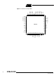
Package Information TQFP80 156 AT8xC5132 4173A–8051–08/02
AT8xC5132 PLCC84 157 4173A–8051–08/02
TQFP64 158 AT8xC5132 4173A–8051–08/02
AT8xC5132 Table of Contents Features ................................................................................................. 1 Description ............................................................................................ 1 Typical Applications ............................................................................. 1 Block Diagram ....................................................................................... 2 Pin Configuration .............................................
Power-down Mode.............................................................................................. 47 Registers............................................................................................................. 49 Timers/Counters ................................................................................. 50 Timer/Counter Operations .................................................................................. 50 Timer Clock Controller .........................................
AT8xC5132 Serial I/O Port .................................................................................... 107 Mode Selection ................................................................................................. 107 Baud Rate Generator........................................................................................ 107 Synchronous Mode (Mode 0) ........................................................................... 108 Asynchronous Modes (Modes 1, 2 and 3) ........................
Atmel Headquarters Atmel Operations Corporate Headquarters Memory 2325 Orchard Parkway San Jose, CA 95131 TEL 1(408) 441-0311 FAX 1(408) 487-2600 Europe Atmel Sarl Route des Arsenaux 41 Case Postale 80 CH-1705 Fribourg Switzerland TEL (41) 26-426-5555 FAX (41) 26-426-5500 Asia Room 1219 Chinachem Golden Plaza 77 Mody Road Tsimhatsui East Kowloon Hong Kong TEL (852) 2721-9778 FAX (852) 2722-1369 Japan 9F, Tonetsu Shinkawa Bldg.