Features • • • • • • • • • • • • • • • • Compatible with MCS-51™ Products 32K Bytes of Reprogrammable Flash Memory Endurance: 1000 Write/Erase Cycles 4V to 5.
pinout. The on-chip Flash allows the program memory to be user programmed by a conventional nonvolatile memory programmer. A total of 512 bytes of internal RAM are available in the AT89C51RC. The 256-byte expanded internal RAM is accessed via MOVX instructions after clearing bit 1 in the SFR located at address 8EH. The other 256-byte RAM segment is accessed the same way as the Atmel AT89-series and other 8052-compatible products.
AT89C51RC The AT89C51RC provides the following standard features: 32K bytes of Flash, 512 bytes of RAM, 32 I/O lines, three 16-bit timer/counters, a six-vector two-level interrupt architecture, a full duplex serial port, on-chip oscillator, and clock circuitry. In addition, the AT89C51RC is designed with static logic for operation down to zero frequency and supports two software selectable power saving modes.
memory. This pin is also the program pulse input (PROG) during Flash programming. In normal operation, ALE is emitted at a constant rate of 1/6 the oscillator frequency and may be used for external timing or clocking purposes. Note, however, that one ALE pulse is skipped during each access to external data memory. If desired, ALE operation can be disabled by setting bit 0 of SFR location 8EH. With the bit set, ALE is active only during a MOVX or MOVC instruction. Otherwise, the pin is weakly pulled high.
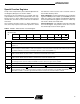
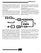
AT89C51RC Special Function Registers A map of the on-chip memory area called the Special Function Register (SFR) space is shown in Table 1. Note that not all of the addresses are occupied, and unoccupied addresses may not be implemented on the chip. Read accesses to these addresses will in general return random data, and write accesses will have an indeterminate effect. User software should not write 1s to these unlisted locations, since they may be used in future products to invoke new features.
Table 3a.
AT89C51RC Memory Organization MCS-51 devices have a separate address space for Program and Data Memory. Up to 64K bytes each of external Program and Data Memory can be addressed. Program Memory If the EA pin is connected to GND, all program fetches are directed to external memory. On the AT89C51RC, if EA is connected to V CC, program fetches to addresses 0000H through 7FFFH are directed to internal memory and fetches to addresses 8000H through FFFFH are to external memory.
Hardware Watchdog Timer (One-time Enabled with Reset-out) The WDT is intended as a recovery method in situations where the CPU may be subjected to software upsets. The WDT consists of a 14-bit counter and the WatchDog Timer Reset (WDTRST) SFR. The WDT is defaulted to disable from exiting reset. To enable the WDT, a user must write 01EH and 0E1H in sequence to the WDTRST register (SFR location 0A6H). When the WDT is enabled, it will increment every machine cycle while the oscillator is running.
AT89C51RC the transition was detected. Since two machine cycles (24 oscillator periods) are required to recognize a 1-to-0 transition, the maximum count rate is 1/24 of the oscillator frequency. To ensure that a given level is sampled at least once before it changes, the level should be held for at least one full machine cycle. current value in TH2 and TL2 to be captured into RCAP2H and RCAP2L, respectively. In addition, the transition at T2EX causes bit EXF2 in T2CON to be set.
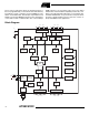
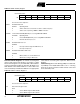
Figure 3. Timer 2 Auto Reload Mode (DCEN = 0) 12 OSC C/T2 = 0 TH2 TL2 OVERFLOW CONTR OL TR2 C/T2 = 1 RELO AD T2 PIN RCAP2H TIMER 2 INTERRUPT RCAP2L TF2 TRANSITION DETECTOR EXF2 T2EX PIN CONTROL EXEN2 Table 5.
AT89C51RC Figure 4. Timer 2 Auto Reload Mode (DCEN = 1) TOGGLE (DOWN COUNTING RELOAD VALUE) 0FFH OSC 0FFH 12 EXF2 OVERFLOW C/T2 = 0 TH2 TL2 TF2 CONTROL TR2 TIMER 2 INTERRUPT C/T2 = 1 T2 PIN RCAP2H RCAP2L COUNT DIRECTION 1=UP 0=DO (UP COUNTING RELOAD VALUE) T2EX PIN Figure 5. Timer 2 in Baud Rate Generator Mode TIMER 1 OVERFLOW ÷2 "0" "1" NOTE: OSC. FREQ.
Baud Rate Generator Timer 2 is selected as the baud rate generator by setting TCLK and/or RCLK in T2CON (Table 2). Note that the baud rates for transmit and receive can be different if Timer 2 is used for the receiver or transmitter and Timer 1 is used for the other function. Setting RCLK and/or TCLK puts Timer 2 into its baud rate generator mode, as shown in Figure 5.
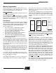
AT89C51RC Programmable Clock Out A 50% duty cycle clock can be programmed to come out on P1.0, as shown in Figure 6. This pin, besides being a regular I/O pin, has two alternate functions. It can be programmed to input the external clock for Timer/Counter 2 or to output a 50% duty cycle clock ranging from 61 Hz to 4 MHz at a 16 MHz operating frequency. To configure the Timer/Counter 2 as a clock generator, bit C/T2 (T2CON.1) must be cleared and bit T2OE (T2MOD.1) must be set. Bit TR2 (T2CON.
Oscillator Characteristics Figure 8. Oscillator Connections XTAL1 and XTAL2 are the input and output, respectively, of an inverting amplifier that can be configured for use as an on-chip oscillator, as shown in Figure 8. Either a quartz crystal or ceramic resonator may be used. To drive the device from an external clock source, XTAL2 should be left unconnected while XTAL1 is driven, as shown in Figure 9.
AT89C51RC Program Memory Lock Bits The AT89C51RC has three lock bits that can be left unprogrammed (U) or can be programmed (P) to obtain the additional features listed in the following table. Table 8.
Programming Interface Every code byte in the Flash array can be programmed by using the appropriate combination of control signals. The write operation cycle is self-timed and once initiated, will automatically time itself to completion. All major programming vendors offer worldwide support for the Atmel microcontroller series. Please contact your local programming vendor for the appropriate software revision. Table 9. Flash Programming Modes Mode VCC RST PSEN P3.4 P2.5-0 P1.
AT89C51RC Flash Programming and Verification Characteristics TA = 20°C to 30°C, VCC = 4.5V to 5.5V Symbol Parameter Min Max Units VPP Programming Supply Voltage 11.5 12.5 V IPP Programming Supply Current 10 mA ICC VCC Supply Current 30 mA 1/tCLCL Oscillator Frequency 33 MHz tAVGL Address Setup to PROG Low 48tCLCL tGHAX Address Hold after PROG 48tCLCL tDVGL Data Setup to PROG Low 48tCLCL tGHDX Data Hold after PROG 48tCLCL tEHSH P2.
Absolute Maximum Ratings* Operating Temperature.................................. -55°C to +125°C *NOTICE: Storage Temperature ..................................... -65°C to +150°C Voltage on Any Pin with Respect to Ground .....................................-1.0V to +7.0V Maximum Operating Voltage ............................................ 6.6V Stresses beyond those listed under “Absolute Maximum Ratings” may cause permanent damage to the device.
AT89C51RC AC Characteristics Under operating conditions, load capacitance for Port 0, ALE/PROG, and PSEN = 100 pF; load capacitance for all other outputs = 80 pF.
External Program Memory Read Cycle tLHLL ALE tAVLL tLLIV tLLPL tPLIV PSEN tPXAV tPLAZ tPXIZ tLLAX tPXIX A0 - A7 PORT 0 tPLPH INSTR IN A0 - A7 tAVIV A8 - A15 PORT 2 A8 - A15 External Data Memory Read Cycle tLHLL ALE tWHLH PSEN tLLDV tRLRH tLLWL RD tLLAX tAVLL PORT 0 tRLDV tRLAZ A0 - A7 FROM RI OR DPL tRHDZ tRHDX DATA IN A0 - A7 FROM PCL INSTR IN tAVWL tAVDV PORT 2 20 P2.0 - P2.
AT89C51RC External Data Memory Write Cycle tLHLL ALE tWHLH PSEN tLLWL WR tAVLL tLLAX tQVWX A0 - A7 FROM RI OR DPL PORT 0 tWLWH tQVWH DATA OUT tWHQX A0 - A7 FROM PCL INSTR IN tAVWL PORT 2 P2.0 - P2.7 OR A8 - A15 FROM DPH A8 - A15 FROM PCH External Clock Drive Waveforms tCHCX VCC - 0.5V tCHCX tCLCH tCHCL 0.7 VCC 0.2 VCC - 0.1V 0.
Serial Port Timing: Shift Register Mode Test Conditions The values in this table are valid for VCC = 4.0V to 5.5V and Load Capacitance = 80 pF. 12 MHz Osc Variable Oscillator Symbol Parameter Min Max Min Max tXLXL Serial Port Clock Cycle Time 1.
AT89C51RC Ordering Information Speed (MHz) Power Supply 24 4.0V to 5.5V 33 Note: 4.5V to 5.5V Ordering Code Package Operation Range AT89C51RC-24AC AT89C51RC-24JC AT89C51RC-24PC 44A 44J 40P6 Commercial (0°C to 70°C) AT89C51RC-24AI AT89C51RC-24JI AT89C51RC-24PI 44A 44J 40P6 Industrial (-40°C to 85°C) AT89C51RC-33AC AT89C51RC-33JC AT89C51RC-33PC 44A 44J 40P6 Commercial (0°C to 70°C) Shaded area indicates preliminary availability.
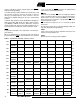
Packaging Information 44A, 44-lead, Thin (1.0 mm) Plastic Gull Wing Quad Flat Package (TQFP) Dimensions in Millimeters and (Inches)* 44J, 44-lead, Plastic J-leaded Chip Carrier (PLCC) Dimensions in Inches and (Millimeters) 12.21(0.478) SQ 11.75(0.458) PIN 1 ID 0.45(0.018) 0.30(0.012) 0.80(0.031) BSC .045(1.14) X 45° PIN NO. 1 IDENTIFY .045(1.14) X 30° - 45° .032(.813) .026(.660) .695(17.7) SQ .685(17.4) .500(12.7) REF SQ 1.20(0.047) MAX 0 7 0.20(.008) 0.09(.003) .630(16.0) .590(15.0) .
Atmel Headquarters Atmel Operations Corporate Headquarters Atmel Colorado Springs 2325 Orchard Parkway San Jose, CA 95131 TEL (408) 441-0311 FAX (408) 487-2600 Europe 1150 E. Cheyenne Mtn. Blvd. Colorado Springs, CO 80906 TEL (719) 576-3300 FAX (719) 540-1759 Atmel Rousset Atmel U.K., Ltd.