Features • 8-bit Microcontroller Compatible with MCS®51 Products • Enhanced 8051 Architecture • • • • • – Single-clock Cycle per Byte Fetch – Up to 20 MIPS Throughput at 20 MHz Clock Frequency – Fully Static Operation: 0 Hz to 20 MHz – On-chip 2-cycle Hardware Multiplier – 128 x 8 Internal RAM – 4-level Interrupt Priority Nonvolatile Program Memory – 2K Bytes of In-System Programmable (ISP) Flash Memory – Endurance: Minimum 10,000 Write/Erase Cycles – Data Retention: Minimum 10 Years – Serial Interfac
have bytes to execute, and most of the remaining instructions require only one additional clock. The enhanced CPU core is capable of 20 MIPS throughput whereas the classic 8051 CPU can deliver only 4 MIPS at the same current consumption. Conversely, at the same throughput as the classic 8051, the new CPU core runs at a much lower speed and thereby greatly reduces power consumption.
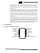
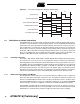
AT89LP216 [Preliminary] 3. Pin Description Table 3-1. Pin 1 AT89LP216 Pin Description Symbol P1.5 Type I/O I/O I 2 P1.7 I/O I/O I Description P1.5: User-configurable I/O Port 1 bit 5. MOSI: SPI master-out/slave-in. When configured as master, this pin is an output. When configured as slave, this pin is an input. GPI5: General-purpose Interrupt input 5. P1.7: User-configurable I/O Port 1 bit 7. SCK: SPI Clock. When configured as master, this pin is an output.
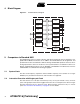
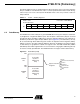
. Block Diagram Figure 4-1. AT89LP216 Block Diagram Single Cycle 8051 CPU UART 2K Bytes Flash SPI 128 Bytes RAM Timer 0 Timer 1 Port 3 Configurable I/O Analog Comparator Port 1 Configurable I/O Watchdog Timer On-Chip RC Oscillator General-purpose Interrupt CPU Clock Configurable Oscillator Crystal or Resonator 5. Comparison to Standard 8051 The AT89LP216 is part of a family of devices with enhanced features that are fully binary compatible with the MCS-51 instruction set.
AT89LP216 [Preliminary] 5.3 Interrupt Handling The interrupt controller polls the interrupt flags during the last clock cycle of any instruction. In order for an interrupt to be serviced at the end of an instruction, its flag needs to have been latched as active during the next to last clock cycle of the instruction, or in the last clock cycle of the previous instruction if the current instruction executes in only a single clock cycle.
5.8 Reset The RST pin of the AT89LP216 is active-low as compared with the active high reset in the standard 8051. In addition, the RST pin is sampled every clock cycle and must be held low for a minimum of two clock cycles, instead of 24 clock cycles, to be recognized as a valid reset. 6. Memory Organization The AT89LP216 uses a Harvard Architecture with separate address spaces for program and data memory.
AT89LP216 [Preliminary] The Atmel Signature Array is initialized with the Device ID in the factory. The User Signature Array is available for user identification codes or constant parameter data. Data stored in the signature array is not secure. Security bits will disable writes to the array; however, reads are always allowed. Table 6-1. AUXR1 – Auxiliary Register 1 AUXR1 = A2H Reset Value = XXXX 0XXXB Not Bit Addressable Bit 6.
7. Special Function Registers A map of the on-chip memory area called the Special Function Register (SFR) space is shown in Table 7-1. Note that not all of the addresses are occupied, and unoccupied addresses may not be implemented on the chip. Read accesses to these addresses will in general return random data, and write accesses will have an indeterminate effect. User software should not write to these unlisted locations, since they may be used in future products to invoke new features. Table 7-1.
AT89LP216 [Preliminary] 8. Enhanced CPU The AT89LP216 uses an enhanced 8051 CPU that runs at 6 to 12 times the speed of standard 8051 devices (or 3 to 6 times the speed of X2 8051 devices). The increase in performance is due to two factors. First, the CPU fetches one instruction byte from the code memory every clock cycle. Second, the CPU uses a simple two-stage pipeline to fetch and execute instructions in parallel. This basic pipelining concept allows the CPU to obtain up to 1 MIPS per MHz.
Figure 8-3. Two-cycle ALU Operation (Example: ADD A, #data) T1 T2 T3 System Clock Total Execution Time Fetch Immediate Operand ALU Operation Execute Result Write Back Fetch Next Instruction 8.1 Restrictions on Certain Instructions The AT89LP216 is an economical and cost-effective member of Atmel's growing family of microcontrollers. It contains 2K bytes of Flash program memory. It is fully compatible with the MCS-51 architecture, and can be programmed using the MCS-51 instruction set.
AT89LP216 [Preliminary] 9. System Clock The system clock is generated directly from one of three selectable clock sources. The three sources are the on-chip crystal oscillator, external clock source, and internal RC oscillator. The clock source is selected by the Clock Source User Fuses as shown in Table 9-1. No internal clock division is used to generate the CPU clock from the system clock. See “User Configuration Fuses” on page 71. Table 9-1. 9.
Table 9-2. CLKREG – Clock Control Register CLKREG = 8FH Reset Value = 0000 0000B Not Bit Addressable Bit Symbol TPS3 TPS2 TPS1 TPS0 TPS3 TPS2 TPS1 TPS0 – CDV1 CDV0 COE 7 6 5 4 3 2 1 0 Function Timer Prescaler. The Timer Prescaler selects the time base for Timer 0, Timer 1 and the Watchdog Timer. The prescaler is implemented as a 4-bit binary down counter. When the counter reaches zero it is reloaded with the value stored in the TPS bits to give a division ratio between 1 and 16.
AT89LP216 [Preliminary] Figure 10-1. Power-on Reset Sequence (BOD Disabled) VPOR VCC VPOR tPOR + tSUT Time-out RST (RST Tied to VCC) Internal Reset RST VRH (RST Controlled Externally) Internal Reset tRHD If the Brown-out Detector (BOD) is also enabled, the start-up timer does not begin counting until after VCC reaches the BOD threshold voltage VBOD as shown in Figure 10-2.
Table 10-1. Start-up Timer Settings SUT Fuse 1 SUT Fuse 0 0 0 Clock Source tSUT (± 5%) µs Internal RC/External Clock 0 Crystal Oscillator 1024 Internal RC/External Clock 512 Crystal Oscillator 2048 Internal RC/External Clock 1024 Crystal Oscillator 4096 Internal RC/External Clock 4096 Crystal Oscillator 16384 1 1 0 1 10.
AT89LP216 [Preliminary] 10.4 Watchdog Reset When the Watchdog times out, it will generate an internal reset pulse lasting 16 clock cycles. Watchdog reset will also set the WDTOVF flag in WDTCON. To prevent a Watchdog reset, the watchdog reset sequence 1EH/E1H must be written to WDTRST before the Watchdog times out. See “Programmable Watchdog Timer” on page 57. for details on the operation of the Watchdog. 10.
When terminating Power-down by an interrupt, two different wake-up modes are available. When PWDEX in PCON is zero, the wake-up period is internally timed as shown in Figure 11-1. At the falling edge on the interrupt pin, Power-down is exited, the oscillator is restarted, and an internal timer begins counting. The internal clock will not be allowed to propagate to the CPU until after the timer has timed out. After the time-out period the interrupt service routine will begin.
AT89LP216 [Preliminary] Figure 11-3. Reset Recovery from Power-down. PWD XTAL1 tSUT RST Internal Clock Internal Reset Table 11-1. PCON – Power Control Register PCON = 87H Reset Value = 000X 0000B Not Bit Addressable Bit SMOD1 SMOD0 PWDEX POF GF1 GF0 PD IDL 7 6 5 4 3 2 1 0 Symbol Function SMOD1 Double Baud Rate bit. Doubles the baud rate of the UART in Modes 1, 2, or 3. SMOD0 Frame Error Select. When SMOD0 = 1, SCON.7 is SM0. When SMOD0 = 1, SCON.7 is FE.
12. Interrupts The AT89LP216 provides 7 interrupt sources: two external interrupts, two timer interrupts, a serial port interrupt, a general-purpose interrupt, and an analog comparator interrupt. These interrupts and the system reset each have a separate program vector at the start of the program memory space. Each interrupt source can be individually enabled or disabled by setting or clearing a bit in the interrupt enable register IE.
AT89LP216 [Preliminary] Table 12-1. 12.1 Interrupt Vector Addresses Interrupt Source Vector Address System Reset RST or POR or BOD 0000H External Interrupt 0 IE0 0003H Timer 0 Overflow TF0 000BH External Interrupt 1 IE1 0013H Timer 1 Overflow TF1 001BH Serial Port RI or TI or SPIF 0023H General-purpose Interrupt GPIF 002BH Analog Comparator CF 0033H Interrupt Response Time The interrupt flags may be set by their hardware in any clock cycle.
Figure 12-1. Minimum Interrupt Response Time Clock Cycles 1 5 INT0 IE0 Instruction Ack. Cur. Instr. LCALL 1st ISR Instr. Figure 12-2. Maximum Interrupt Response Time Clock Cycles 1 13 INT0 Ack. IE0 Instruction Table 12-2. RETI 4 Cyc. Instr. LCALL 1st ISR In IE – Interrupt Enable Register IE = A8H Reset Value = 0000 0000B Bit Addressable Bit EA EC EGP ES ET1 EX1 ET0 EX0 7 6 5 4 3 2 1 0 Symbol Function EA Global enable/disable. All interrupts are disabled when EA = 0.
AT89LP216 [Preliminary] Table 12-3. IP – Interrupt Priority Register IP = B8H Reset Value = X000 0000B Bit Addressable Bit – – PGP PS PT1 PX1 PT0 PX0 7 6 5 4 3 2 1 0 Symbol Function PGP General-purpose Interrupt Priority Low PS Serial Port Interrupt Priority Low PT1 Timer 1 Interrupt Priority Low PX1 External Interrupt 1 Priority Low PT0 Timer 0 Interrupt Priority Low PX0 External Interrupt 0 Priority Low Table 12-4.
13. I/O Ports The AT89LP216 can be configured for between 9 and 12 I/O pins. The exact number of I/O pins available depends on the clock and reset options as shown in Table 13-1. All port pins are 5V tolerant, that is they can be pulled up or driven to 5.5V even when operating at a lower VCC such as 3V. Table 13-1.
AT89LP216 [Preliminary] 13.1.1 Quasi-bidirectional Output Port pins in quasi-bidirectional output mode function similar to standard 8051 port pins. A Quasibidirectional port can be used both as an input and output without the need to reconfigure the port. This is possible because when the port outputs a logic high, it is weakly driven, allowing an external device to pull the pin low. When the pin is driven low, it is driven strongly and able to sink a large current.
13.1.2 Input-only Mode The input only port configuration is shown in Figure 13-2. The output drivers are tristated. The input includes a Schmitt-triggered input for improved input noise rejection. The input circuitry of P1.3, P3.2 and P3.3 is not disabled during Power-down (see Figure 13-3). Input pins can be safely driven to 5.5V even when operating at lower VCC levels; however, the input threshold of the Schmitt trigger will be set by the VCC level and must be taken into consideration. Figure 13-2.
AT89LP216 [Preliminary] Figure 13-5. Push-pull Output VCC Port Pin From Port Register Input Data PWD 13.2 Port 1 Analog Functions The AT89LP216 incorporates an analog comparator. In order to give the best analog performance and minimize power consumption, pins that are being used for analog functions must have both their digital outputs and digital inputs disabled. Digital outputs are disabled by putting the port pins into the input-only mode as described in “Port Configuration” on page 22.
13.4 Port Alternate Functions Most general-purpose digital I/O pins of the AT89LP216 share functionality with the various I/Os needed for the peripheral units. Table 13-5 lists the alternate functions of the port pins. Alternate functions are connected to the pins in a logic AND fashion. In order to enable the alternate function on a port pin, that pin must have a “1” in its corresponding port register bit, otherwise the input/output will always be “0”.
AT89LP216 [Preliminary] 14. Enhanced Timer/Counters The AT89LP216 has two 16-bit Timer/Counter registers: Timer 0 and Timer 1. As a Timer, the register increase every clock cycle by default. Thus, the register counts clock cycles. Since a clock cycle consists of one oscillator period, the count rate is equal to the oscillator frequency. The timer rate can be prescaled by a value between 1 and 16 using the Timer Prescaler (see Table 9-2 on page 12). Both Timers share the same prescaler.
Figure 14-1. Timer/Counter 1 Mode 0: Variable Width Counter OSC ÷TPS C/T = 0 TL1 (8 Bits) C/T = 1 T1 Pin Control PSC1 TR1 TH1 (8 Bits) GATE Interrupt TF1 INT1 Pin Mode 0 operation is the same for Timer 0 as for Timer 1, except that TR0, TF0 and INT0 replace the corresponding Timer 1 signals in Figure 14-1. There are two different GATE bits, one for Timer 1 (TMOD.7) and one for Timer 0 (TMOD.3). The INT0 and INT1 pins are shared with the XTAL oscillator.
AT89LP216 [Preliminary] 14.3 Mode 2 – 8-bit Auto-Reload Timer/Counter Mode 2 configures the Timer register as an 8-bit Counter (TL1) with automatic reload, as shown in Figure 14-3. Overflow from TL1 not only sets TF1, but also reloads TL1 with the contents of TH1, which is preset by software. The reload leaves TH1 unchanged. Mode 2 operation is the same for Timer/Counter 0.
. Table 14-1. TCON – Timer/Counter Control Register TCON = 88H Reset Value = 0000 0000B Bit Addressable Bit TF1 TR1 TF0 TR0 IE1 IT1 IE0 IT0 7 6 5 4 3 2 1 0 Symbol Function TF1 Timer 1 overflow flag. Set by hardware on Timer/Counter overflow. Cleared by hardware when the processor vectors to interrupt routine. TR1 Timer 1 run control bit. Set/cleared by software to turn Timer/Counter on/off. TF0 Timer 0 overflow flag. Set by hardware on Timer/Counter overflow.
AT89LP216 [Preliminary] Table 14-2. TMOD: Timer/Counter Mode Control Register TMOD = 88H Reset Value = 0000 0000B Not Bit Addressable GATE C/T M1 M0 GATE C/T M1 M0 7 6 5 4 3 2 1 0 Timer1 Timer0 Gate Gating control when set. Timer/Counter x is enabled only while INTx pin is high and TRx control pin is set. When cleared, Timer x is enabled whenever TRx control bit is set. Timer 0 gate bit C/T Timer or Counter Selector cleared for Timer operation (input from internal system clock).
. Table 14-3. TCONB – Timer/Counter Control Register B TCONB = 91H Reset Value = 0010 0100B Not Bit Addressable Bit PWM1EN PWM0EN PSC12 PSC11 PSC10 PSC02 PSC01 PSC00 7 6 5 4 3 2 1 0 Symbol Function PWM1EN Configures Timer 1 for Pulse Width Modulation output on T1 (P3.5). PWM0EN Configures Timer 0 for Pulse Width Modulation output on T0 (P3.4). PSC12 PSC11 PSC10 Prescaler for Timer 1 Mode 0. The number of active bits in TL1 equals PSC1 + 1.
AT89LP216 [Preliminary] 14.5.1 Mode 0 – 8-bit PWM with 8-bit Logarithmic Prescaler In Mode 0, TLx acts as a logarithmic prescaler driving 8-bit counter THx (see Figure 14-6). The PSCx bits in TCONB control the prescaler value. On THx overflow, the duty cycle value in RHx is transferred to OCRx and the output pin is set high. When the count in THx matches OCRx, the output pin is cleared low. The following formulas give the output frequency and duty cycle for Timer 0 in PWM Mode 0.
Figure 14-7. Timer/Counter 1 PWM Mode 1 RH1 (8 Bits) RL1 (8 Bits) OCR1 = T1 OSC TH1 (8 Bits) TL1 (8 Bits) ÷TPS Control TR1 GATE INT1 Pin 14.5.3 Mode 2 – 8-bit Frequency Generator Timer 0 in PWM Mode 2 functions as an 8-bit Auto-Reload timer, the same as normal Mode 2, with the exception that the output pin T0 is toggled at every TL0 overflow (see Figure 14-8). Timer 1 in PWM Mode 2 is identical to Timer 0. PWM Mode 2 can be used to output a square wave of varying frequency.
AT89LP216 [Preliminary] 14.5.4 Mode 3 – Split 8-bit PWM Timer 1 in PWM Mode 3 simply holds its count. The effect is the same as setting TR1 = 0. Timer 0 in PWM Mode 3 establishes TL0 and TH0 as two separate PWM counters in a manner similar to normal Mode 3. PWM Mode 3 on Timer 0 is shown in Figure 14-9. Only the Timer Prescaler is available to change the output frequency during PWM Mode 3. TL0 can use the Timer 0 control bits: GATE, TR0, INT0, PWM0EN and TF0.
15. External Interrupts When the AT89LP216 is configured to use the internal RC Oscillator, XTAL1 and XTAL2 may be used as the INT0 and INT1 external interrupt sources. The external interrupts can be programmed to be level-activated or transition-activated by setting or clearing bit IT1 or IT0 in Register TCON. If ITx = 0, external interrupt x is triggered by a detected low at the INTx pin. If ITx = 1, external interrupt x is edge-triggered.
AT89LP216 [Preliminary] Table 16-2. GPLS – General-purpose Interrupt Level Select Register GPLS = 9BH Reset Value = 0000 0000B Not Bit Addressable GPLS7 GPLS6 GPLS5 GPLS4 GPLS3 GPLS2 GPLS1 GPLS0 7 6 5 4 3 2 1 0 Bit GPMOD.x 0 = detect low level or negative edge on P1.x 1 = detect high level or positive edge on P1.x . Table 16-3.
17. Serial Interface The serial interface on the AT89LP216 implements a Universal Asynchronous Receiver/Transmitter (UART). The UART has the following features: • Full-duplex Operation • 8 or 9 Data Bits • Framing Error Detection • Multiprocessor Communication Mode with Automatic Address Recognition • Baud Rate Generator Using Timer 1 • Interrupt on Receive Buffer Full or Transmission Complete The serial interface is full-duplex, which means it can transmit and receive simultaneously.
AT89LP216 [Preliminary] bit and prepares to receive the data bytes that follows. The slaves that are not addressed set their SM2 bits and ignore the data bytes. The SM2 bit has no effect in Mode 0 but can be used to check the validity of the stop bit in Mode 1. In a Mode 1 reception, if SM2 = 1, the receive interrupt is not activated unless a valid stop bit is received. Table 17-1.
17.2 Baud Rates The baud rate in Mode 0 is fixed as shown in the following equation: Oscillator Frequency Mode 0 Baud Rate = ------------------------------------------------------2 The baud rate in Mode 2 depends on the value of the SMOD1 bit in Special Function Register PCON.7. If SMOD1 = 0 (the value on reset), the baud rate is 1/32 of the oscillator frequency.
AT89LP216 [Preliminary] Table 17-2 lists commonly used baud rates and how they can be obtained from Timer 1. Table 17-2. Commonly Used Baud Rates Generated by Timer 1 (TPS = 0000B) Timer 1 17.3 Baud Rate fOSC (MHz) SMOD1 C/T Mode Reload Value Mode 0: 1 MHz 2 X X X X Mode 2: 375K 12 0 X X X 62.5K 12 1 0 2 F4H 19.2K 11.059 1 0 2 DCH 9.6K 11.059 0 0 2 DCH 4.8K 11.059 0 0 2 B8H 2.4K 11.059 0 0 2 70H 1.2K 11.059 0 0 1 FEE0H 137.5 11.
Figure 17-1.
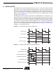
AT89LP216 [Preliminary] 17.4 More About Mode 1 Ten bits are transmitted (through TXD), or received (through RXD): a start bit (0), 8 data bits (LSB first), and a stop bit (1). On receive, the stop bit goes into RB8 in SCON. In the AT89LP216, the baud rate is determined by the Timer 1 overflow rate. Figure 17-2 shows a simplified functional diagram of the serial port in Mode 1 and associated timings for transmit and receive.
Figure 17-2. Serial Port Mode 1 TIMER 1 OVERFLOW INTERNAL BUS “1” WRITE TO SBUF ÷2 SMOD1 =1 SMOD1 =0 S D Q CL SBUF TXD ZERO DETECTOR SHIFT DATA START TX CONTROL ÷16 RX CLOCK SEND TI SERIAL PORT INTERRUPT ÷16 SAMPLE 1-TO-0 TRANSITION DETECTOR RX CLOCK RI START RX CONTROL LOAD SBUF SHIFT 1FFH BIT DETECTOR INPUT SHIFT REG.
AT89LP216 [Preliminary] 17.5 More About Modes 2 and 3 Eleven bits are transmitted (through TXD), or received (through RXD): a start bit (0), 8 data bits (LSB first), a programmable 9th data bit, and a stop bit (1). On transmit, the 9th data bit (TB8) can be assigned the value of “0” or “1”. On receive, the 9th data bit goes into RB8 in SCON. The baud rate is programmable to either 1/16 or 1/32 of the oscillator frequency in Mode 2. Mode 3 may have a variable baud rate generated from Timer 1.
Figure 17-3.
AT89LP216 [Preliminary] Figure 17-4. Serial Port Mode 3 TIMER 1 OVERFLOW INTERNAL BUS TB8 WRITE TO SBUF ÷2 SMOD1 = 1 SMOD1 = 0 S D Q CL SBUF TXD ZERO DETECTOR ÷16 SHIFT DATA START STOP BIT TX CONTROL RX CLOCK SEND TI SERIAL PORT INTERRUPT ÷16 SAMPLE 1-TO-0 TRANSITION DETECTOR RX CLOCK RI START RX CONTROL LOAD SBUF SHIFT 1FFH BIT DETECTOR INPUT SHIFT REG.
17.6 Framing Error Detection In addition to all of its usual modes, the UART can perform framing error detection by looking for missing stop bits, and automatic address recognition. When used for framing error detect, the UART looks for missing stop bits in the communication. A missing bit will set the FE bit in the SCON register. The FE bit shares the SCON.7 bit with SM0 and the function of SCON.7 is determined by PCON.6 (SMOD0). If SMOD0 is set then SCON.7 functions as FE. SCON.
AT89LP216 [Preliminary] In a more complex system, the following could be used to select slaves 1 and 2 while excluding slave 0: Slave 0 SADDR = 1100 0000 SADEN = 1111 1001 Given = 1100 0XX0 Slave 1 SADDR = 1110 0000 SADEN = 1111 1010 Given = 1110 0X0X Slave 2 SADDR = 1110 0000 SADEN = 1111 1100 Given = 1110 00XX In the above example, the differentiation among the 3 slaves is in the lower 3 address bits. Slave 0 requires that bit 0 = 0 and it can be uniquely addressed by 1110 0110.
The interconnection between master and slave CPUs with SPI is shown in Figure 18-1. The four pins in the interface are Master-In/Slave-Out (MISO), Master-Out/Slave-In (MOSI), Shift Clock (SCK), and Slave Select (SS). The SCK pin is the clock output in master mode, but is the clock input in slave mode. The MSTR bit in SPCR determines the directions of MISO and MOSI. Also notice that MOSI connects to MOSI and MISO to MISO. In master mode, SS/P1.
AT89LP216 [Preliminary] Table 18-1. SPCR – SPI Control Register SPCR Address = E9H Reset Value = 0000 0000B Not Bit Addressable Bit SPIE SPE DORD MSTR CPOL CPHA SPR1 SPR0 7 6 5 4 3 2 1 0 Symbol Function SPIE SPI interrupt enable. This bit, in conjunction with the ES bit in the IE register, enables SPI interrupts: SPIE = 1 and ES = 1 enable SPI interrupts. SPIE = 0 disables SPI interrupts. SPE SPI enable.
Table 18-3. SPSR – SPI Status Register SPSR Address = E8H Reset Value = 000X X000B Not Bit Addressable Bit SPIF WCOL LDEN – – SSIG DISSO ENH 7 6 5 4 3 2 1 0 Symbol Function SPIF SP interrupt flag. When a serial transfer is complete, the SPIF bit is set and an interrupt is generated if SPIE = 1 and ES = 1. The SPIF bit is cleared by reading the SPI status register followed by reading/writing the SPI data register. WCOL When ENH = 0: Write collision flag.
AT89LP216 [Preliminary] Figure 18-2. SPI Shift Register Diagram 7 Serial In Serial Master 8 2:1 MUX D Serial Slave 2:1 MUX Q D LATCH Q Serial Out LATCH CLK CLK 8 Parallel Master Transmit Byte Parallel Slave (Write Buffer) 8 D (Read Buffer) 8 Q D LATCH 8 Q Receive Byte LATCH CLK CLK Figure 18-3. SPI Block Diagram S Oscillator MSB LSB Pin Control Logic Read Data Buffer Divider ÷4÷8÷32÷64 Write Data Buffer Clock SPI Clock (Mater) SCK 1.
The CPHA (Clock PHAse), CPOL (Clock POLarity), and SPR (Serial Peripheral clock Rate = baud rate) bits in SPCR control the shape and rate of SCK. The two SPR bits provide four possible clock rates when the SPI is in master mode. In slave mode, the SPI will operate at the rate of the incoming SCK as long as it does not exceed the maximum bit rate. There are also four possible combinations of SCK phase and polarity with respect to the serial data. CPHA and CPOL determine which format is used for transmission.
AT89LP216 [Preliminary] 19. Analog Comparator A single analog comparator is provided on the AT89LP216. The analog comparator has the following features: • Comparator Output Flag and Interrupt • Selectable Interrupt Condition – High- or Low-level – Rising- or Falling-edge – Output Toggle • Hardware Debouncing Modes Comparator operation is such that the output is a logic “1” when the positive input AIN0 (P1.0]) is greater than the negative input AIN1 (P1.1). Otherwise the output is a zero.
Table 19-1. ACSR – Analog Comparator Control & Status Register ACSR = 97H Reset Value = XXX0 0000B Not Bit Addressable Bit – – CIDL CF CEN CM3 CM1 CM0 7 6 5 4 3 2 1 0 Symbol Function CIDL Comparator Idle Enable. If CIDL = 1 the comparator will continue to operate during Idle mode. If CIDL = 0 the comparator is powered down during Idle mode. The comparator is always shut down during Power-down mode. CF Comparator Interrupt Flag.
AT89LP216 [Preliminary] 20. Programmable Watchdog Timer The programmable Watchdog Timer (WDT) protects the system from incorrect execution by triggering a system reset when it times out after the software has failed to feed the timer prior to the timer overflow. By Default the WDT counts CPU clock cycles. The prescaler bits, PS0, PS1 and PS2 in SFR WDTCON are used to set the period of the Watchdog Timer from 16K to 2048K clock cycles.
20.1 Software Reset A Software Reset of the AT89LP216 is accomplished by writing the software reset sequence 5AH/A5H to the WDTRST SFR. The WDT does not need to be enabled to generate the software reset. A normal software reset will set the SWRST flag in WDTCON. However, if at any time an incorrect sequence is written to WDTRST (i.e. anything other than 1EH/E1H or 5AH/A5H), a software reset will immediately be generated and both the SWRST and WDTOVF flags will be set.
AT89LP216 [Preliminary] 21. Instruction Set Summary The AT89LP216 is fully binary compatible with the MCS-51 instruction set. The difference between the AT89LP216 and the standard 8051 is the number of cycles required to execute an instruction. Instructions in the AT89LP216 may take 1, 2, 3 or 4 clock cycles to complete. The execution times of most instructions may be computed using Table 21-1. Table 21-1.
Table 21-1.
AT89LP216 [Preliminary] Table 21-1.
Table 21-1.
AT89LP216 [Preliminary] 22. On-Chip Debug System The AT89LP216 On-Chip Debug (OCD) System uses a two-wire serial interface to control program flow; read, modify, and write the system state; and program the nonvolatile memory.
22.2 Software Breakpoints The AT89LP216 microcontroller includes a BREAK instruction for implementing program memory breakpoints in software. A software breakpoint can be inserted manually by placing the BREAK instruction in the program code. Some emulator systems may allow for automatic insertion/deletion of software breakpoints. The Flash memory must be re-programmed each time a software breakpoint is changed.
AT89LP216 [Preliminary] 23. Programming the Flash Memory The Atmel AT89LP216 microcontroller features 2K bytes of on-chip In-System Programmable Flash program memory. In-System Programming allows programming and reprogramming of the microcontroller positioned inside the end system. Using a simple 4-wire SPI interface, the InSystem programmer communicates serially with the AT89LP216 microcontroller, reprogramming all nonvolatile memories on the chip.
The In-System Programming Interface is the only means of externally programming the AT89LP216 microcontroller. The ISP Interface can be used to program the device both in-system and in a standalone serial programmer. The ISP Interface does not require any clock other than SCK and is not limited by the system clock frequency. During In-System Programming the system clock source of the target device can operate normally.
AT89LP216 [Preliminary] Figure 23-2. AT89LP216 Memory Organization User Fuse Row Page 0 User Signature Array Page 1 Atmel Signature Array Page 0 Page 0 07FF Page 63 Page 62 Code Memory Page 1 Page 0 00 23.3 0000 1F Command Format Programming commands consist of an opcode byte, two address bytes, and zero or more data bytes. In addition, all command packets must start with a two-byte preamble of AAH and 55H.
Figure 23-3. Command Sequence Flow Chart Input Preamble 1 (AAh) Input Preamble 2 (55h) Input Opcode Input Address High Byte Input Address Low Byte Input/Output Data Address +1 Figure 23-4.
AT89LP216 [Preliminary] Table 23-2. Programming Command Summary Command Opcode Addr High Addr Low Data 0 Data n Program Enable(1) 1010 1100 0101 0011 – – – Chip Erase 1000 1010 – – – – Read Status 0110 0000 xxxx xxxx xxxx xxxx Status Out Load Page Buffer(2) 0101 0001 xxxx xxxx xxxb bbbb DataIn 0 ... DataIn n Write Code Page(2) 0101 0000 xxxx xaaa aaab bbbb DataIn 0 ... DataIn n Write Code Page with Auto-Erase(2) 0111 0000 xxxx xaaa aaab bbbb DataIn 0 ...
23.4 Status Register The current state of the memory may be accessed by reading the status register. The status register is shown in Table 23-3. Table 23-3. Bit Status Register – – – – LOAD SUCCESS WRTINH BUSY 7 6 5 4 3 2 1 0 Symbol Function LOAD Load flag. Cleared low by the load page buffer command and set high by the next memory write. This flag signals that the page buffer was previously loaded with data by the load page buffer command. SUCCESS Success flag.
AT89LP216 [Preliminary] 23.7 User Configuration Fuses The AT89LP216 includes 19 user fuses for configuration of the device. Each fuse is accessed at a separate address in the User Fuse Row as listed in Table 23-5. Fuses are cleared by programming 00h to their locations. Programming FFh to fuse location will cause that fuse to maintain its previous state. To set a fuse (set to FFh) the fuse row must be erased and then reprogrammed using the Fuse Write with Auto-erase command.
23.8 Programming Interface Timing This section details general system timing sequences and constraints for entering or exiting InSystem Programming as well as parameters related to the Serial Peripheral Interface during ISP. The general timing parameters for the following waveform figures are listed in section “Timing Parameters” on page 75. 23.8.1 Power-up Sequence Execute this sequence to enter programming mode immediately after power-up.
AT89LP216 [Preliminary] 23.8.3 ISP Start Sequence Execute this sequence to exit CPU execution mode and enter ISP mode when the device has passed Power-On Reset and is already operational. 1. Drive RST low. 2. Drive SS high. 3. Wait tRLZ + tSTL. 4. Start programming session. Figure 23-7. In-System Programming (ISP) Start Sequence tRLZ VCC XTAL1 RST tSTL SS tZSS tSSE SCK 23.8.4 MISO HIGH Z MOSI HIGH Z ISP Exit Sequence Execute this sequence to exit ISP mode and resume CPU execution mode. 1.
23.8.5 Serial Peripheral Interface The Serial Peripheral Interface (SPI) is a byte-oriented full-duplex synchronous serial communication channel. During In-System Programming, the programmer always acts as the SPI master and the target device always acts as the SPI slave. The target device receives serial data on MOSI and outputs serial data on MISO.
AT89LP216 [Preliminary] 23.8.6 Timing Parameters The timing parameters for Figure 23-5, Figure 23-6, Figure 23-7, Figure 23-8, and Figure 23-10 are shown in Table . Table 23-6.
24. Electrical Characteristics 24.1 Absolute Maximum Ratings* Operating Temperature ................................... -40°C to +85°C *NOTICE: Storage Temperature ..................................... -65°C to +150°C Voltage on Any Pin with Respect to Ground......-0.7V to +5.5V Maximum Operating Voltage ............................................ 5.5V DC Output Current...................................................... 15.0 mA 24.
AT89LP216 [Preliminary] 24.3 Serial Peripheral Interface Timing Table 24-1. SPI Master Characteristics Symbol Parameter Min tCLCL Oscillator Period 41.
Figure 24-1. SPI Master Timing (CPHA = 0) SS tSR tSCK SCK (CPOL = 0) SCK (CPOL = 1) tSF tSHSL tSLSH tSLSH tSHSL tSIS tSIH MISO tSOH tSOV MOSI Figure 24-2. SPI Slave Timing (CPHA = 0) SS tSR tSCK tSSE SCK (CPOL = 0) SCK (CPOL= 1) tSHSL tSLSH tSLSH tSHSL tSOV tSOE tSSD tSF tSOX tSOH MISO tSIS tSIH MOSI Figure 24-3.
AT89LP216 [Preliminary] Figure 24-4. SPI Slave Timing (CPHA = 1) SS tSCK tSSE SCK (CPOL = 0) SCK (CPOL = 1) tSR tSF tSHSL tSLSH tSLSH tSHSL tSOE tSOV tSSD tSOX tSOH MISO tSIS tSIH MOSI 24.4 External Clock Drive Figure 24-5. External Clock Drive Waveform VCC = 2.4V to 5.
24.5 Serial Port Timing: Shift Register Mode The values in this table are valid for VCC = 2.4V to 5.5V and Load Capacitance = 80 pF. Variable Oscillator Symbol Parameter Min Max Units tXLXL Serial Port Clock Cycle Time 2tCLCL -15 µs tQVXH Output Data Setup to Clock Rising Edge tCLCL -15 ns tXHQX Output Data Hold after Clock Rising Edge tCLCL -15 ns tXHDX Input Data Hold after Clock Rising Edge 0 ns tXHDV Input Data Valid to Clock Rising Edge 15 ns Figure 24-6.
AT89LP216 [Preliminary] 24.6.3 ICC Test Condition, Active Mode, All Other Pins are Disconnected VCC ICC RST XTAL2 (NC) CLOCK SIGNAL 24.6.4 VCC XTAL1 VSS ICC Test Condition, Idle Mode, All Other Pins are Disconnected VCC ICC RST XTAL2 (NC) CLOCK SIGNAL 24.6.5 VCC XTAL1 VSS Clock Signal Waveform for ICC Tests in Active and Idle Modes, tCLCH = tCHCL = 5 ns VCC - 0.5V 0.45V 0.7 VCC tCHCX 0.2 VCC - 0.1V tCHCL tCLCH tCHCX tCLCL 24.6.
25. Ordering Information 25.1 Standard Package Speed (MHz) Power Supply 20 2.4V to 5.5V 25.2 Ordering Code Package AT89LP216-20PI AT89LP216-20SI AT89LP216-20XI 16P3 16S2 16X Operation Range Industrial (-40° C to 85° C) Green Package Option (Pb/Halide-free) Speed (MHz) Power Supply 20 2.4V to 5.5V Ordering Code Package AT89LP216-20PU AT89LP216-20SU AT89LP216-20XU 16P3 16S2 16X Operation Range Industrial (-40° C to 85° C) Package Types 16P3 16-lead, 0.
AT89LP216 [Preliminary] 26. Packaging Information 26.1 16P3 – PDIP D PIN 1 E1 A A1 SEATING PLANE L B1 e B2 B COMMON DIMENSIONS (Unit of Measure = mm) E C eB Notes: eC 1. This package conforms to JEDEC reference MS-001, Variation AB. 2. Dimensions D and E1 do not include mold Flash or Protrusion. Mold Flash or Protrusion shall not exceed 0.25 mm (0.010"). SYMBOL MIN NOM MAX A – – 5.334 A1 0.381 – – D 19.81 – 20.32 E 7.620 – 8.255 E1 6.096 – 7.112 B 0.356 – 0.
26.2 16S2 – SOIC C 1 H L E N A1 Top View End View e COMMON DIMENSIONS (Unit of Measure = inches) b A D Side View SYMBOL MIN NOM MAX NOTE A 0.0926 0.1043 A1 0.0040 0.0118 b 0.0130 0.0200 C 0.0091 0.0125 D 0.3977 0.4133 2 E 0.2914 0.2992 3 H 0.3940 0.4190 L 0.0160 0.050 e 5 4 0.050 BSC Notes: 1. This drawing is for general information only; refer to JEDEC Drawing MS-013, Variation AA for additional information. 2.
AT89LP216 [Preliminary] 26.3 16X – TSSOP C 1 E1 End View E L Top View e Ø b COMMON DIMENSIONS (Unit of Measure = mm) A A1 SYMBOL D Side View MIN NOM MAX A – – 1.20 A1 0.05 – 0.15 b 0.19 – 0.30 C 0.09 – 0.20 D 4.90 5.00 5.10 E1 4.30 4.40 4.50 E 6.40 BSC e 0.65 TYP L 0.45 0.60 0.75 Ø 0o – 8o NOTE Note: These drawings are for general information only. Refer to JEDEC Drawing MO-153-AB.
27. Revision History 86 Revision No.
AT89LP216 [Preliminary] Table of Contents 1. Description ............................................................................................... 1 2. Pin Configuration ..................................................................................... 2 2.1 AT89LP216: 16-lead PDIP/SOIC/TSSOP ..............................................................2 3. Pin Description ......................................................................................... 3 4. Block Diagram ..........
Table of Contents (Continued) 12. Interrupts ................................................................................................ 18 12.1 Interrupt Response Time ......................................................................................19 13. I/O Ports .................................................................................................. 22 13.1 Port Configuration .................................................................................................22 13.
AT89LP216 [Preliminary] Table of Contents (Continued) 23. Programming the Flash Memory .......................................................... 65 23.1 Physical Interface .................................................................................................65 23.2 Memory Organization ...........................................................................................66 23.3 Command Format .................................................................................................
Atmel Corporation 2325 Orchard Parkway San Jose, CA 95131, USA Tel: 1(408) 441-0311 Fax: 1(408) 487-2600 Regional Headquarters Europe Atmel Sarl Route des Arsenaux 41 Case Postale 80 CH-1705 Fribourg Switzerland Tel: (41) 26-426-5555 Fax: (41) 26-426-5500 Asia Room 1219 Chinachem Golden Plaza 77 Mody Road Tsimshatsui East Kowloon Hong Kong Tel: (852) 2721-9778 Fax: (852) 2722-1369 Japan 9F, Tonetsu Shinkawa Bldg.