
Manual

AT89LS53
4-252
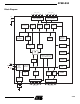
Pin Description
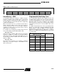
Furthermore, P1.4, P1.5, P1.6, and P1.7 can be configured
as the SPI slave port select, data input/output and shift
clock input/output pins as shown in the following table.
Port 1 also receives the low-order address bytes during
Flash programming and verification.
Port 2
Port 2 is an 8-bit bidirectional I/O port with internal pullups.
The Port 2 output buffers can sink/source four TTL inputs.
When 1s are written to Port 2 pins, they are pulled high by
the internal pullups and can be used as inputs. As inputs,
Port 2 pins that are externally being pulled low will source
current (I
IL
) because of the internal pullups.
Port 2 emits the high-order address byte during fetches
from external program memory and during accesses to
external data memory that use 16-bit addresses (MOVX @
DPTR). In this application, Port 2 uses strong internal pul-
lups when emitting 1s. During accesses to external data
memory that use 8-bit addresses (MOVX @ RI), Port 2
emits the contents of the P2 Special Function Register.
Port 2 also receives the high-order address bits and some
control signals during Flash programming and verification.
Port 3
Port 3 is an 8 bit bidirectional I/O port with internal pullups.
The Port 3 output buffers can sink/source four TTL inputs.
When 1s are written to Port 3 pins, they are pulled high by
the internal pullups and can be used as inputs. As inputs,
Port 3 pins that are externally being pulled low will source
current (I
IL
) because of the pullups.
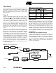
Port 3 also serves the functions of various special features
of the AT89LS53, as shown in the following table.
Port 3 also receives some control signals for Flash pro-
gramming and verification.
RST
Reset input. A high on this pin for two machine cycles while
the oscillator is running resets the device.
ALE/PROG
Address Latch Enable is an output pulse for latching the
low byte of the address during accesses to external mem-
ory. This pin is also the program pulse input (PROG
) during
Flash programming.
In normal operation, ALE is emitted at a constant rate of 1/
6 the oscillator frequency and may be used for external tim-
ing or clocking purposes. Note, however, that one ALE
pulse is skipped during each access to external data mem-
ory.
If desired, ALE operation can be disabled by setting bit 0 of
SFR location 8EH. With the bit set, ALE is active only dur-
ing a MOVX or MOVC instruction. Otherwise, the pin is
weakly pulled high. Setting the ALE-disable bit has no
effect if the microcontroller is in external execution mode.
PSEN
Program Store Enable is the read strobe to external pro-
gram memory.
When the AT89LS53 is executing code from external pro-
gram memory, PSEN
is activated twice each machine
cycle, except that two PSEN
activations are skipped during
each access to external data memory.
EA
/V
PP
External Access Enable. EA must be strapped to GND in
order to enable the device to fetch code from external pro-
gram memory locations starting at 0000H up to FFFFH.
Note, however, that if lock bit 1 is programmed, EA
will be
internally latched on reset.
EA
should be strapped to V
CC
for internal program execu-
tions. This pin also receives the 12-volt programming
enable voltage (V
PP
) during Flash programming when 12-
volt programming is selected.
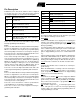
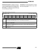
Port Pin Alternate Functions
P1.0
T2 (external count input to Timer/Counter
2), clock-out
P1.1
T2EX (Timer/Counter 2 capture/reload
trigger and direction control)
P1.4 SS
(Slave port select input)
P1.5
MOSI (Master data output, slave data input
pin for SPI channel)
P1.6
MISO (Master data input, slave data output
pin for SPI channel)
P1.7
SCK (Master clock output, slave clock input
pin for SPI channel)
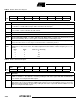
Port Pin Alternate Functions
P3.0 RXD (serial input port)
P3.1 TXD (serial output port)
P3.2 INT0
(external interrupt 0)
P3.3 INT1
(external interrupt 1)
P3.4 T0 (timer 0 external input)
P3.5 T1 (timer 1 external input)
P3.6 WR
(external data memory write strobe)
P3.7 RD
(external data memory read strobe)