
Manual

AT89LS53
4-255
Dual Data Pointer Registers
To facilitate accessing exter-
nal data memory, two banks of 16 bit Data Pointer Regis-
ters are provided: DP0 at SFR address locations 82H-83H
and DP1 at 84H-85H. Bit DPS = 0 in SFR WCON selects
DP0 and DPS = 1 selects DP1. The user should always ini-
talize the DPS bit to the appropriate value before accessing
the respective Data Pointer register.
Power Off Flag
The Power Off Flag (POF) is located at
bit_4 (PCON.4) in the PCON SFR. POF is set to “1” during
power up. It can be set and reset under software control
and is not affected by RESET.
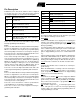
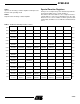
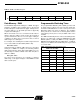
Table 3.
WCON—Watchdog Control Register
WCON Address = 96H Reset Value = 0000 0010B
PS2 PS1 PS0 reserved reserved DPS WDTRST WDTEN
Bit76543210
Symbol Function
PS2
PS1
PS0
Prescaler Bits for the Watchdog Timer. When all three bits are set to “0”, the watchdog timer has a nominal
period of 16 ms. When all three bits are set to “1”, the nominal period is 2048 ms.
DPS Data Pointer Register Select. DPS = 0 selects the first bank of Data Pointer Register, DP0, and DPS = 1
selects the second bank, DP1
WDTRST Watchdog Timer Reset. Each time this bit is set to “1” by user software, a pulse is generated to reset the
watchdog timer. The WDTRST bit is then automatically reset to “0” in the next instruction cycle. The
WDTRST bit is Write-Only.
WDTEN Watchdog Timer Enable Bit. WDTEN = 1 enables the watchdog timer and WDTEN = 0 disables the
watchdog timer.