Features • Compatible with MCS-51™ Products • 20K Bytes of Reprogrammable Flash Memory • • • • • • • • – Endurance: 1,000 Write/Erase Cycles Fully Static Operation: 0 Hz to 12 MHz Three-level Program Memory Lock 256 x 8-bit Internal RAM 32 Programmable I/O Lines Three 16-bit Timer/Counters Eight Interrupt Sources Low-power Idle and Power-down Modes 2.7V to 6.
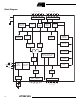
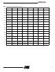
Block Diagram P0.0 - P0.7 P2.0 - P2.7 PORT 0 DRIVERS PORT 2 DRIVERS VCC GND RAM ADDR. REGISTER B REGISTER PORT 0 LATCH RAM PORT 2 LATCH FLASH STACK POINTER ACC PROGRAM ADDRESS REGISTER BUFFER TMP2 TMP1 PC INCREMENTER ALU INTERRUPT, SERIAL PORT, AND TIMER BLOCKS PROGRAM COUNTER PSW PSEN ALE/PROG EA / VPP TIMING AND CONTROL INSTRUCTION REGISTER DPTR RST PORT 1 LATCH PORT 3 LATCH PORT 1 DRIVERS PORT 3 DRIVERS OSC P1.0 - P1.7 2 AT89LV55 P3.0 - P3.
AT89LV55 The AT89LV55 provides the following standard features: 20K bytes of Flash, 256 bytes of RAM, 32 I/O lines, three 16-bit timer/counters, a six-vector two-level interrupt architecture, a full duplex serial port, on-chip oscillator, and clock circuitry. In addition, the AT89LV55 is designed with static logic for operation down to zero frequency and supports two software selectable power saving modes.
ALE/PROG Address Latch Enable is an output pulse for latching the low byte of the address during accesses to external memory. This pin is also the program pulse input (PROG) during Flash programming. In normal operation, ALE is emitted at a constant rate of 1/6 the oscillator frequency and may be used for external timing or clocking purposes. Note, however, that one ALE pulse is skipped during each access to external data memory.
AT89LV55 Table 1.
Table 2. T2CON – Timer/Counter 2 Control Register T2CON Address = 0C8H Reset Value = 0000 0000B Bit Addressable Bit TF2 EXF2 RCLK TCLK EXEN2 TR2 C/T2 CP/RL2 7 6 5 4 3 2 1 0 Symbol Function TF2 Timer 2 overflow flag set by a Timer 2 overflow and must be cleared by software. TF2 will not be set when either RCLK = 1 or TCLK = 1. EXF2 Timer 2 external flag set when either a capture or reload is caused by a negative transition on T2EX and EXEN2 = 1.
AT89LV55 Capture Mode In the capture mode, two options are selected by bit EXEN2 in T2CON. If EXEN2 = 0, Timer 2 is a 16-bit timer or counter which upon overflow sets bit TF2 in T2CON. This bit can then be used to generate an interrupt. If EXEN2 = 1, Timer 2 performs the same operation, but a 1- to-0 transition at external input T2EX also causes the current value in TH2 and TL2 to be captured into RCAP2H and RCAP2L, respectively. In addition, the transition at T2EX causes bit EXF2 in T2CON to be set.
Figure 2. Timer 2 Auto Reload Mode (DCEN = 0) Table 4. T2MOD—Timer 2 Mode Control Register T2MOD Address = 0C9H Reset Value = XXXX XX00B Not Bit Addressable Bit 8 — — — — — — T20E DCEN 7 6 5 4 3 2 1 0 Symbol Function — Not implemented, reserved for future use. T20E Timer 2 Output Enable bit. DCEN When set, this bit allows Timer 2 to be configured as an up/down counter.
AT89LV55 Figure 3. Timer 2 Auto Reload Mode (DCEN = 1) (DOWN COUNTING RELOAD VALUE) 0FFH OSC ÷12 TOGGLE 0FFH EXF2 OVERFLOW C/T2 = 0 TH2 TL2 TF2 CONTROL TR2 C/T2 = 1 TIMER 2 INTERRUPT T2 PIN RCAP2H RCAP2L (UP COUNTING RELOAD VALUE) COUNT DIRECTION 1=UP 0=DOWN T2EX PIN Figure 4.
Baud Rate Generator Timer 2 is selected as the baud rate generator by setting TCLK and/or RCLK in T2CON (Table 2). Note that the baud rates for transmit and receive can be different if Timer 2 is used for the receiver or transmitter and Timer 1 is used for the other function. Setting RCLK and/or TCLK puts Timer 2 into its baud rate generator mode, as shown in Figure 4.
AT89LV55 Programmable Clock Out A 50% duty cycle clock can be programmed to come out on P1.0, as shown in Figure 5. This pin, besides being a regular I/O pin, has two alternate functions. It can be programmed to input the external clock for Timer/Counter 2 or to output a 50% duty cycle clock ranging from 61 Hz to 3 MHz at a 12 MHz operating frequency. To configure the Timer/Counter 2 as a clock generator, bit C/T2 (T2CON.1) must be cleared and bit T2OE (T2MOD.1) must be set. Bit TR2 (T2CON.
Oscillator Characteristics Figure 7. Oscillator Connections XTAL1 and XTAL2 are the input and output, respectively, of an inverting amplifier that can be configured for use as an on-chip oscillator, as shown in Figure 7. Either a quartz crystal or ceramic resonator may be used. To drive the device from an external clock source, XTAL2 should be left unconnected while XTAL1 is driven, as shown in Figure 8.
AT89LV55 Power Down Mode Program Memory Lock Bits In the power down mode, the oscillator is stopped, and the instruction that invokes power down is the last instruction executed. The on-chip RAM and Special Function Registers retain their values until the power down mode is terminated. The only exit from power down is a hardware reset. Reset redefines the SFRs but does not change the on-chip RAM.
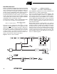
Figure 9. Programming the Flash Memory Figure 10. Verifying the Flash Memory +5V +5V AT89LV55 A0 - A7 ADDR. 0000H/4FFFH A8 - A13 A14* SEE FLASH PROGRAMMING MODES TABLE AT89LV55 P1.0 - P1.7 VCC P2.0 - P2.5 P3.0 P2.6 P2.7 P0 ALE PGM DATA PROG P3.6 ADDR. 0000H/4FFFH A8 - A13 A14* SEE FLASH PROGRAMMING MODES TABLE EA VI H/VPP 3-12 MHz VCC P2.0 - P2.5 P0 P3.0 P2.6 P2.7 PGM DATA (USE 10K PULLUPS) ALE P3.
AT89LV55 Flash Programming Modes EA/VPP P2.6 P2.7 P3.6 P3.7 12V L H H H H L L H H L 12V H H H H H L 12V H H L L H L 12V H L H L Chip Erase H L 12V H L L L Read Signature Byte H L H L L L L Mode RST PSEN Write Code Data H L Read Code Data H L Bit-1 H Bit-2 Bit-3 Write Lock Note: 1. ALE/PROG H (1) H Chip Erase requires a 10 ms PROG pulse.
Flash Programming and Verification Characteristics TA = 0°C to 70°C, VCC = 5.0V ± 10% Symbol Parameter Min Max Units VPP Programming Enable Voltage 11.5 12.5 V IPP Programming Enable Current 1.0 mA 1/tCLCL Oscillator Frequency 12 MHz tAVGL Address Setup to PROG Low 48tCLCL tGHAX Address Hold After PROG 48tCLCL tDVGL Data Setup to PROG Low 48tCLCL tGHDX Data Hold After PROG 48tCLCL tEHSH P2.
AT89LV55 Absolute Maximum Ratings* Operating Temperature ................................. -55°C to +125°C *NOTICE: Storage Temperature ..................................... -65°C to +150°C Voltage on Any Pin with Respect to Ground .....................................-1.0V to +7.0V Maximum Operating Voltage ............................................ 6.6V Stresses beyond those listed under “Absolute Maximum Ratings” may cause permanent damage to the device.
AC Characteristics Under operating conditions, load capacitance for Port 0, ALE/PROG, and PSEN = 100 pF; load capacitance for all other outputs = 80 pF.
AT89LV55 External Program Memory Read Cycle External Data Memory Read Cycle 19
External Data Memory Write Cycle External Clock Drive Waveforms External Clock Drive Symbol Parameter 1/tCLCL Oscillator Frequency tCLCL Clock Period tCHCX Min Max Units 0 12 MHz 83.
AT89LV55 Serial Port Timing: Shift Register Mode Test Conditions The values in this table are valid for VCC = 5.0V ± 20% and Load Capacitance = 80 pF. Symbol Parameter 12 MHz Osc Min Variable Oscillator Max Min Units Max tXLXL Serial Port Clock Cycle Time 1.
Notes: 22 1. XTAL1 tied to GND for ICC (power down) 2.
AT89LV55 Ordering Information Speed (MHz) Power Supply 12 2.7V - 6.0V Ordering Code Package Operation Range AT89LV55-12AC AT89LV55-12JC AT89LV55-12PC 44A 44J 40P6 Commercial (0°C to 70°C) AT89LV55-12AI AT89LV55-12JI AT89LV55-12PI 44A 44J 40P6 Industrial (-40°C to 85°C) Package Type 44A 44 Lead, Thin Plastic Gull Wing Quad Flatpack (TQFP) 44J 44 Lead, Plastic J-Leaded Chip Carrier (PLCC) 40P6 40 Lead, 0.
Atmel Headquarters Atmel Operations Corporate Headquarters Atmel Colorado Springs 2325 Orchard Parkway San Jose, CA 95131 TEL (408) 441-0311 FAX (408) 487-2600 Europe Atmel SarL Route des Arsenaux 41 Casa Postale 80 CH-1705 Fribourg Switzerland TEL (41) 26-426-5555 FAX (41) 26-426-5500 Asia Atmel Asia, Ltd. Room 1219 Chinachem Golden Plaza 77 Mody Road Tsimhatsui East Kowloon Hong Kong TEL (852) 2721-9778 FAX (852) 2722-1369 Japan 1150 E. Cheyenne Mtn. Blvd.