Features • Utilizes the AVR® RISC Architecture • AVR – High-performance and Low-power RISC Architecture • • • • • • • • – 118 Powerful Instructions – Most Single Clock Cycle Execution – 32 x 8 General-purpose Working Registers – Up to 10 MIPS Throughput at 10 MHz Data and Nonvolatile Program Memory – 2K Bytes of In-System Programmable Flash Endurance: 1,000 Write/Erase Cycles – 128 Bytes Internal RAM – 128 Bytes of In-System Programmable EEPROM Endurance: 100,000 Write/Erase Cycles – Programming Lock
Description The AT90S/LS2323 and AT90S/LS2343 are low-power, CMOS, 8-bit microcontrollers based on the AVR RISC architecture. By executing powerful instructions in a single clock cycle, the AT90S2323/2343 achieves throughputs approaching 1 MIPS per MHz allowing the system designer to optimize power consumption versus processing speed. The AVR core combines a rich instruction set with 32 general-purpose working registers.
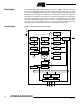
AT90S/LS2323/2343 Figure 2. The AT90S/LS2323 Block Diagram VCC 8-BIT DATA BUS INTERNAL OSCILLATOR GND PROGRAM COUNTER STACK POINTER WATCHDOG TIMER PROGRAM FLASH SRAM MCU CONTROL REGISTER INSTRUCTION REGISTER INSTRUCTION DECODER CONTROL LINES TIMING AND CONTROL RESET TIMER/ COUNTER GENERAL PURPOSE REGISTERS X Y Z INTERRUPT UNIT ALU EEPROM STATUS REGISTER PROGRAMMING LOGIC SPI OSCILLATOR DATA REGISTER PORTB DATA DIR. REG.
chip, the Atmel AT90S2323/2343 is a powerful microcontroller that provides a highly flexible and cost-effective solution to many embedded control applications. The AT90S2323/2343 AVR is supported with a full suite of program and system development tools including: C compilers, macro assemblers, program debugger/simulators, in-circuit emulators and evaluation kits.
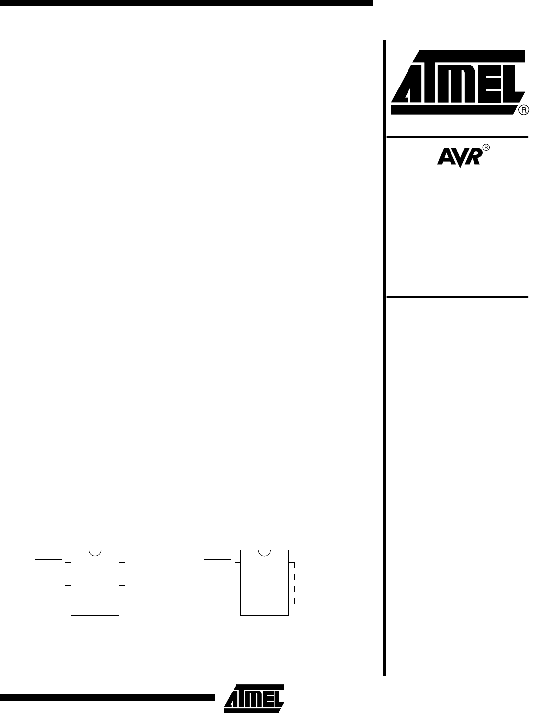
AT90S/LS2323/2343 Pin Descriptions AT90S/LS2343 VCC Supply voltage pin. GND Ground pin. Port B (PB4..PB0) Port B is a 5-bit bi-directional I/O port with internal pull-up resistors. The Port B output buffers can sink 20 mA. As inputs, Port B pins that are externally pulled low, will source current if the pull-up resistors are activated. Port B also serves the functions of various special features. Port pins can provide internal pull-up resistors (selected for each bit).
Figure 4.
AT90S/LS2323/2343 Architectural Overview The fast-access register file concept contains 32 x 8-bit general-purpose working registers with a single clock cycle access time. This means that during one single clock cycle, one ALU (Arithmetic Logic Unit) operation is executed. Two operands are output from the register file, the operation is executed and the result is stored back in the register file – in one clock cycle.
The AVR has Harvard architecture – with separate memories and buses for program and data. The program memory is accessed with a two-stage pipeline. While one instruction is being executed, the next instruction is pre-fetched from the program memory. This concept enables instructions to be executed in every clock cycle. The program memory is in-system downloadable Flash memory. With the relative jump and call instructions, the whole 1K address space is directly accessed.
AT90S/LS2323/2343 General-purpose Register File Figure 7 shows the structure of the 32 general-purpose registers in the CPU. Figure 7. AVR CPU General-purpose Working Registers 7 0 Addr.
X-register, Y-register and Zregister The registers R26..R31 have some added functions to their general-purpose usage. These registers are the address pointers for indirect addressing of the Data Space. The three indirect address registers X, Y, and Z, are defined in Figure 8. Figure 8.
AT90S/LS2323/2343 SRAM Data Memory Figure 9 shows how the AT90S2323/2343 Data Memory is organized. Figure 9. SRAM Organization Register File Data Address Space R0 $00 R1 $01 R2 $02 … … R29 $1D R30 $1E R31 $1F I/O Registers $00 $20 $01 $21 $02 $22 … … $3D $5D $3E $5E $3F $5F Internal SRAM $60 $61 $62 … $DD $DE $DF The 224 data memory locations address the Register file, I/O memory and the data SRAM.
Program and Data Addressing Modes The AT90S2323/2343 AVR RISC microcontroller supports powerful and efficient addressing modes for access to the program memory (Flash) and data memory. This section describes the different addressing modes supported by the AVR architecture. In the figures, OP means the operation code part of the instruction word. To simplify, not all figures show the exact location of the addressing bits. Register Direct, Single Register Rd Figure 10.
AT90S/LS2323/2343 I/O Direct Figure 12. I/O Direct Addressing Operand address is contained in six bits of the instruction word. n is the destination or source register address. Data Direct Figure 13. Direct Data Addressing A 16-bit data address is contained in the 16 LSBs of a 2-word instruction. Rd/Rr specify the destination or source register. Data Indirect with Displacement Figure 14.
Data Indirect Figure 15. Data Indirect Addressing Operand address is the contents of the X-, Y-, or the Z-register. Data Indirect with Predecrement Figure 16. Data Indirect Addressing with Pre-decrement The X-, Y-, or the Z-register is decremented before the operation. Operand address is the decremented contents of the X-, Y-, or the Z-register. Data Indirect with Postincrement Figure 17. Data Indirect Addressing with Post-increment +1 The X-, Y-, or the Z-register is incremented after the operation.
AT90S/LS2323/2343 Constant Addressing Using the LPM Instruction Figure 18. Code Memory Constant Addressing Constant byte address is specified by the Z-register contents. The 15 MSBs select word address (0 - 1K), the LSB selects low byte if cleared (LSB = 0) or high byte if set (LSB = 1). Indirect Program Addressing, IJMP and ICALL Figure 19. Indirect Program Memory Addressing Program execution continues at address contained by the Z-register (i.e., the PC is loaded with the contents of the Z-register).
Memory Access and Instruction Execution Timing This section describes the general access timing concepts for instruction execution and internal memory access. The AVR CPU is driven by the System Clock Ø, directly generated from the external clock signal applied to the CLOCK pin. No internal clock division is used. Figure 21. shows the parallel instruction fetches and instruction executions enabled by the Harvard architecture and the fast-access register file concept.
AT90S/LS2323/2343 Figure 23. On-chip Data SRAM Access Cycles T1 T2 Prev. Address Address T3 T4 System Clock Ø Address Write Data WR Read Data RD I/O Memory The I/O space definition of the AT90S2323/2343 is shown in Table 2. Table 2.
and OUT, the I/O addresses $00 - $3F must be used. When addressing I/O registers as SRAM, $20 must be added to these addresses. All I/O register addresses throughout this document are shown with the SRAM address in parentheses. For compatibility with future devices, reserved bits should be written to zero if accessed. Reserved I/O memory addresses should never be written. Some of the status flags are cleared by writing a logical “1” to them.
AT90S/LS2323/2343 • Bit 0 – C: Carry Flag The carry flag C indicates a carry in an arithmetical or logical operation. See the Instruction Set description for detailed information. Note that the Status Register is not automatically stored when entering an interrupt routine and restored when returning from an interrupt routine. This must be handled by software. Stack Pointer – SPL An 8- bit r egister at I/O addres s $3D ( $5D) for ms the stack pointer of the AT90S2323/2343.
The most typical program setup for the Reset and Interrupt vector addresses are: Address Code Comments $000 Labels rjmp RESET ; Reset Handler $001 rjmp EXT_INT0 ; IRQ0 Handler $002 rjmp TIM_OVF0 ; Timer0 Overflow ; Handler; ldi r16, low(RAMEND) ; Main program start $003 MAIN: out SPL, r16 xxx ... Reset Sources ... ... ... The AT90S2323/2343 provides three sources of reset: • Power-on Reset. The MCU is reset when the supply voltage is below the Power-on Reset threshold (VPOT).
AT90S/LS2323/2343 Table 4. Reset Characteristics (VCC = 5.0V) Symbol VPOT(1) Parameter Min Typ Max Units Power-on Reset Threshold Voltage, rising 1.0 1.4 1.8 V Power-on Reset Threshold Voltage, falling 0.4 0.6 0.8 V VRST RESET Pin Threshold Voltage tTOUT Reset Delay Time-out Period AT90S/LS2323 FSTRT Programmed 1.0 1.1 1.2 ms tTOUT Reset Delay Time-out Period AT90S/LS2323 FSTRT Unprogrammed 11.0 16.0 21.0 ms tTOUT Reset Delay Time-out Period AT90S/LS2343 11.0 16.0 21.
Figure 25. MCU Start-up, RESET Tied to VCC. VCC RESET VPOT VRST tTOUT TIME-OUT INTERNAL RESET Figure 26. MCU Start-up, RESET Controlled Externally VCC RESET VPOT VRST TIME-OUT tTOUT INTERNAL RESET External Reset An external reset is generated by a low level on the RESET pin. Reset pulses longer than 50 ns will generate a reset, even if the clock is not running. Shorter pulses are not guaranteed to generate a reset.
AT90S/LS2323/2343 Watchdog Reset When the Watchdog times out, it will generate a short reset pulse of 1 CPU clock cycle duration. On the falling edge of this pulse, the delay timer starts counting the Time-out period tTOUT. Refer to page 30 for details on operation of the Watchdog. Figure 28. Watchdog Reset during Operation MCU Status Register – MCUSR The MCU Status Register provides information on which reset source caused an MCU reset.
Table 8. Reset Source Identification Interrupt Handling PORF EXTRF Reset Source 0 0 Watchdog Reset 0 1 External Reset 1 0 Power-on Reset 1 1 Power-on Reset The AT90S2323/2343 has two 8-bit interrupt mask control registers; GIMSK (General Interrupt Mask register) and TIMSK (Timer/Counter Interrupt Mask register). When an interrupt occurs, the Global Interrupt Enable I-bit is cleared (zero) and all interrupts are disabled. The user software can set (one) the I-bit to enable nested interrupts.
AT90S/LS2323/2343 General Interrupt Flag Register – GIFR Bit 7 6 5 4 3 2 1 0 $3A ($5A) – INTF0 – – – – – – Read/Write R R/W R R R R R R Initial Value 0 0 0 0 0 0 0 0 GIFR • Bit 7 – Res: Reserved Bit This bit is a reserved bit in the AT90S2323/2343 and always reads as zero. • Bit 6 – INTF0: External Interrupt Flag0 When an edge on the INT0 pin triggers an interrupt request, the corresponding interrupt flag, INTF0 becomes set (one).
• Bit 0 – Res: Reserved Bit This bit is a reserved bit in the AT90S2323/2343 and always reads zero. External Interrupt The external interrupt is triggered by the INT0 pin. Observe that, if enabled, the interrupt will trigger even if the INT0 pin is configured as an output. This feature provides a way of generating a software interrupt. The external interrupt can be triggered by a falling or rising edge or a low level. This is set up as indicated in the specification for the MCU Control Register (MCUCR).
AT90S/LS2323/2343 activate the interrupt are defined in Table 9. The value on the INT01 pin is sampled before detecting edges. If edge or toggle interrupt is selected, pulses that last longer than one clock period will generate an interrupt. Shorter pulses are not guaranteed to generate an interrupt. If low-level interrupt is selected, the low level must be held until the completion of the currently executing instruction to generate an interrupt. Table 9.
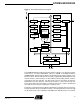
Timer/Counter The AT90S2323/2343 provides one general-purpose 8-bit Timer/Counter – Timer/Counter0. The Timer/Counter has prescaling selection from the 10-bit prescaling timer. The Timer/Counter can be used either as a timer with an internal clock time base or as a counter with an external pin connection that triggers the counting. Timer/Counter Prescaler Figure 29 shows the Timer/Counter prescaler. Figure 29.
AT90S/LS2323/2343 Figure 30. Timer/Counter 0 Block Diagram T0 Timer/Counter0 Control Register – TCCR0 Bit 7 6 5 4 3 2 1 0 $33 ($53) – – – – – CS02 CS01 CS00 Read/Write R R R R R R/W R/W R/W Initial Value 0 0 0 0 0 0 0 0 TCCR0 • Bits 7..3 – Res: Reserved Bits These bits are reserved bits in the AT90S2323/2343 and always read zero.
The Stop condition provides a Timer Enable/Disable function. The CK down divided modes are scaled directly from the CK oscillator clock. If the external pin modes are used for Timer/Counter0, transitions on PB2/(T0) will clock the counter even if the pin is configured as an output. This feature can give the user software control of the counting.
AT90S/LS2323/2343 Watchdog Timer Control Register – WDTCR Bit 7 6 5 4 3 2 1 0 $21 ($41) – – – WDTOE WDE WDP2 WDP1 WDP0 Read/Write R R R R/W R/W R/W R/W R/W Initial Value 0 0 0 0 0 0 0 0 WDTCR • Bits 7..5 – Res: Reserved Bits These bits are reserved bits in the AT90S2323/2343 and will always read as zero. • Bit 4 – WDTOE: Watchdog Turn-off Enable This bit must be set (one) when the WDE bit is cleared. Otherwise, the Watchdog will not be disabled.
EEPROM Read/Write Access The EEPROM access registers are accessible in the I/O space. The write access time is in the range of 2.5 - 4 ms, depending on the VCC voltages. A self-timing function, however, lets the user software detect when the next byte can be written. In order to prevent unintentional EEPROM writes, a specific write procedure must be followed. Refer to the description of the EEPROM Control Register for details on this.
AT90S/LS2323/2343 EEPROM Control Register – EECR Bit 7 6 5 4 3 2 1 0 $1C ($3C) – – – – – EEMWE EEWE EERE Read/Write R R R R R R/W R/W R/W Initial Value 0 0 0 0 0 0 0 0 EECR • Bits 7..3 – Res: Reserved Bits These bits are reserved bits in the AT90S2323/2343 and will always read as zero. • Bit 2 – EEMWE: EEPROM Master Write Enable The EEMWE bit determines whether setting EEWE to “1” causes the EEPROM to be written.
Prevent EEPROM Corruption During periods of low VCC, the EEPROM data can be corrupted because the supply voltage is too low for the CPU and the EEPROM to operate properly. These issues are the same as for board level systems using the EEPROM and the same design solutions should be applied. An EEPROM data corruption can be caused by two situations when the voltage is too low. First, a regular write sequence to the EEPROM requires a minimum voltage to operate correctly.
AT90S/LS2323/2343 I/O Port B All AVR ports have true read-modify-write functionality when used as general digital I/O ports. This means that the direction of one port pin can be changed without unintentionally changing the direction of any other pin with the SBI and CBI instructions. The same applies for changing drive value (if configured as output) or enabling/disabling of pull-up resistors (if configured as input). For the AT90S/LS2323, Port B is an 3-bit bi-directional I/O port.
Port B Input Pins Address – PINB Bit 7 6 5 4 3 2 1 0 $16 ($36) – – – PINB4 PINB3 PINB2 PINB1 PINB0 Read/Write R R R R R R R R Initial Value 0 0 0 N/A N/A N/A N/A N/A PINB The Port B Input Pins address (PINB) is not a register and this address enables access to the physical value on each Port B pin. When reading PORTB, the Port B Data Latch is read and when reading PINB, the logical values present on the pins are read.
AT90S/LS2323/2343 Memory Programming Program and Data Memory Lock Bits The AT90S2323/2343 MCU provides two Lock bits that can be left unprogrammed (“1”) or can be programmed (“0”) to obtain the additional features listed in Table 14. The Lock bits can only be erased with the Chip Erase operation. Table 14. Lock Bit Protection Modes Memory Lock Bits Mode LB1 LB2 1 1 1 No memory lock features enabled. 2 0 1 Further programming of the Flash and EEPROM is disabled.
3. $002: $03 (indicates AT90S/LS2343 when signature byte $001 is $91) Note: Programming the Flash and EEPROM When both Lock bits are programmed (Lock mode 3), the signature bytes cannot be read in the low-voltage Serial mode. Reading the signature bytes will return: $00, $01 and $02. Atmel’s AT90S2323/2343 offers 2K bytes of In-System Programmable Flash program memory and 128 bytes of EEPROM data memory.
AT90S/LS2323/2343 High-voltage Serial Programming Algorithm To program and verify the AT90S/LS2323 and AT90S/LS234 in the high-voltage Serial Programming mode, the following sequence is recommended (see instruction formats in Table 16): 1. Power-up sequence: Apply 4.5 - 5.5V between VCC and GND. Set RESET and PB0 to “0” and wait at least 100 ns. Then, if the RCEN Fuse is not programmed, toggle XTAL1/PB3 at least four times with minimum 100 ns pulse width. Set PB3 to “0”. Wait at least 100 ns.
Table 16. High-voltage Serial Programming Instruction Set Instruction Format Instruction Instr.1 Instr.2 Instr.3 Instr.
AT90S/LS2323/2343 Table 16. High-voltage Serial Programming Instruction Set (Continued) Instruction Format Instruction Instr.1 Instr.2 Instr.3 Instr.
High-voltage Serial Programming Characteristics Figure 34. High-voltage Serial Programming Timing SDI (PB0), SII (PB1) tIVSH SCI (XTAL1/PB3) tSHIX tSLSH tSHSL SDO (PB2) tSHOV Table 17. High-voltage Serial Programming Characteristics, TA = 25°C ± 10%, VCC = 5.0V ± 10% (unless otherwise noted) Symbol Low-voltage Serial Downloading Parameter Min Typ Max Units tSHSL SCI (XTAL1/PB3) Pulse Width High 100.0 ns tSLSH SCI (XTAL1/PB3) Pulse Width Low 100.
AT90S/LS2323/2343 For the EEPROM, an auto-erase cycle is provided within the self-timed Write instruction and there is no need to first execute the Chip Erase instruction. The Chip Erase instruction turns the content of every memory location in both the program and EEPROM arrays into $FF. The program and EEPROM memory arrays have separate address spaces: $0000 to $03FF for Flash program memory and $000 to $07F for EEPROM data memory.
7. At the end of the programming session, RESET can be set high to commence normal operation. 8. Power-off sequence (if needed): Set CLOCK/XTAL1 to “0”. Set RESET to “1”. Turn VCC power off. Data Polling EEPROM When a byte is being programmed into the EEPROM, reading the address location being programmed will give the value P1 until the auto-erase is finished, and then the value P2 will be given. See Table 18 for P1 and P2 values.
AT90S/LS2323/2343 Table 19. Low-voltage Serial Programming Instruction Set AT90S2323/2343 Instruction Format Instruction Byte 1 Byte 2 Byte 3 Byte 4 1010 1100 0101 0011 xxxx xxxx xxxx xxxx Enable Serial programming while RESET is low. 1010 1100 100x xxxx xxxx xxxx xxxx xxxx Chip erase both Flash and EEPROM memory arrays. 0010 H000 0000 00aa bbbb bbbb oooo oooo Read H (high or low) data o from program memory at word address a:b.
Low-voltage Serial Programming Characteristics Figure 37. Low-voltage Serial Programming Timing MOSI tOVSH SCK tSLSH tSHOX tSHSL MISO tSLIV Table 20. Low-voltage Serial Programming Characteristics, TA = -40°C to 85°C, VCC = 2.7 - 6.0V (unless otherwise noted) Symbol Parameter Min 1/tCLCL Oscillator Frequency (VCC = 2.7 - 4.0V) tCLCL Oscillator Period (VCC = 2.7 - 4.0V) 1/tCLCL Oscillator Frequency (VCC = 4.0 - 6.0V) tCLCL Oscillator Period (VCC = 4.0 - 6.0V) tSHSL Typ 0 Max Units 4.
AT90S/LS2323/2343 Electrical Characteristics Absolute Maximum Ratings* Operating Temperature.................................. -55°C to +125°C *NOTICE: Stresses beyond those listed under “Absolute Maximum Ratings” may cause permanent damage to the device. This is a stress rating only and functional operation of the device at these or other conditions beyond those indicated in the operational sections of this specification is not implied.
External Clock Drive Waveforms Figure 38. Waveforms VIH1 VIL1 External Clock Drive TA = -40°C to 85°C VCC: 2.7V to 4.0V Symbol 1/tCLCL 48 Parameter Oscillator Frequency VCC: 4.0V to 6.0V Min Max Min Max Units 0 4.0 0 10.0 MHz tCLCL Clock Period 250.0 100.0 ns tCHCX High Time 100.0 40.0 ns tCLCX Low Time 100.0 40.0 ns tCLCH Rise Time 1.6 0.5 µs tCHCL Fall Time 1.6 0.
AT90S/LS2323/2343 Typical Characteristics The following charts show typical behavior. These figures are not tested during manufacturing. All current consumption measurements are performed with all I/O pins configured as inputs and with internal pull-ups enabled. A sine wave generator with railto-rail output is used as clock source.
Figure 40. Active Supply Current vs. VCC ACTIVE SUPPLY CURRENT vs. Vcc FREQUENCY = 4 MHz 10 9 TA = 25˚C 8 TA = 85˚C 7 I cc(mA) 6 5 4 3 2 1 0 2 2.5 3 3.5 4 4.5 5 5.5 6 Vcc(V) Figure 41. Active Supply Current vs. VCC ACTIVE SUPPLY CURRENT vs. Vcc DEVICE CLOCKED BY INTERNAL RC OSCILLATOR 7 6 TA = 25˚C 5 I cc(mA) TA = 85˚C 4 3 2 1 0 2 2.5 3 3.5 4 4.5 5 5.
AT90S/LS2323/2343 Figure 42. Idle Supply Current vs. Frequency IDLE SUPPLY CURRENT vs. FREQUENCY TA= 25˚C 5 Vcc= 6V 4.5 Vcc= 5.5V 4 Vcc= 5V 3.5 I cc(mA) 3 Vcc= 4.5V 2.5 Vcc= 4V Vcc= 3.6V 2 Vcc= 3.3V 1.5 Vcc= 3.0V 1 Vcc= 2.7V 0.5 0 0 1 2 3 4 5 6 7 8 9 10 11 12 13 14 15 Frequency (MHz) Figure 43. Idle Supply Current vs. VCC IDLE SUPPLY CURRENT vs. Vcc FREQUENCY = 4 MHz 2.5 2 TA = 25˚C I cc(mA) TA = 85˚C 1.5 1 0.5 0 2 2.5 3 3.5 4 4.5 5 5.
Figure 44. Idle Supply Current vs. VCC IDLE SUPPLY CURRENT vs. Vcc DEVICE CLOCKED BY INTERNAL RC OSCILLATOR 0.8 0.7 TA = 25˚C 0.6 I cc(mA) 0.5 TA = 85˚C 0.4 0.3 0.2 0.1 0 2 2.5 3 3.5 4 4.5 5 5.5 6 Vcc(V) Figure 45. Power-down Supply Current vs. VCC POWER DOWN SUPPLY CURRENT vs. Vcc WATCHDOG TIMER DISABLED 25 TA = 85˚C 20 I cc(µΑ) 15 TA = 70˚C 10 5 TA = 45˚C TA = 25˚C 0 2 2.5 3 3.5 4 4.5 5 5.
AT90S/LS2323/2343 Figure 46. Power-down Supply Current vs. VCC POWER DOWN SUPPLY CURRENT vs. Vcc WATCHDOG TIMER ENABLED 180 160 TA = 85˚C 140 I cc(µΑ) 120 TA = 25˚C 100 80 60 40 20 0 2 2.5 3 3.5 4 4.5 5 5.5 6 Vcc(V) Figure 47. Watchdog Oscillator Frequency vs. VCC WATCHDOG OSCILLATOR FREQUENCY vs. Vcc 1600 TA = 25˚C 1400 TA = 85˚C F RC (KHz) 1200 1000 800 600 400 200 0 2 2.5 3 3.5 4 4.5 5 5.
Note: Sink and source capabilities of I/O ports are measured on one pin at a time. Figure 48. Pull-up Resistor Current vs. Input Voltage PULL-UP RESISTOR CURRENT vs. INPUT VOLTAGE Vcc = 5V 120 TA = 25˚C 100 TA = 85˚C I OP (µA) 80 60 40 20 0 0 0.5 1 1.5 2 2.5 VOP (V) 3 3.5 4 4.5 5 Figure 49. Pull-up Resistor Current vs. Input Voltage PULL-UP RESISTOR CURRENT vs. INPUT VOLTAGE Vcc = 2.7V 30 TA = 25˚C 25 TA = 85˚C 15 I OP (µA) 20 10 5 0 0 0.5 1 1.5 2 2.
AT90S/LS2323/2343 Figure 50. I/O Pin Sink Current vs. Output Voltage I/O PIN SINK CURRENT vs. OUTPUT VOLTAGE Vcc = 5V 70 TA = 25˚C 60 TA = 85˚C 50 30 I OL (mA) 40 20 10 0 0 0.5 1 1.5 2 2.5 3 VOL (V) Figure 51. I/O PIn Source Current vs. Output Voltage I/O PIN SOURCE CURRENT vs. OUTPUT VOLTAGE Vcc = 5V 20 TA = 25˚C 18 16 TA = 85˚C 14 I OH (mA) 12 10 8 6 4 2 0 0 0.5 1 1.5 2 2.5 3 3.5 4 4.
Figure 52. I/O Pin Sink Current vs. Output Voltage I/O PIN SINK CURRENT vs. OUTPUT VOLTAGE Vcc = 2.7V 25 TA = 25˚C 20 TA = 85˚C 10 I OL (mA) 15 5 0 0 0.5 1 1.5 2 VOL (V) Figure 53. I/O Pin Source Current vs. Output voltage I/O PIN SOURCE CURRENT vs. OUTPUT VOLTAGE Vcc = 2.7V 6 TA = 25˚C 5 TA = 85˚C 3 I OH (mA) 4 2 1 0 0 0.5 1 1.5 2 2.
AT90S/LS2323/2343 Figure 54. I/O Pin Input Threshold Voltage vs. VCC I/O PIN INPUT THRESHOLD VOLTAGE vs. Vcc TA = 25˚C 2.5 Threshold Voltage (V) 2 1.5 1 0.5 0 2.7 4.0 5.0 Vcc Figure 55. I/O Pin Input Hysteresis vs. VCC I/O PIN INPUT HYSTERESIS vs. Vcc TA = 25˚C 0.18 0.16 Input hysteresis (V) 0.14 0.12 0.1 0.08 0.06 0.04 0.02 0 2.7 4.0 5.
AT90S2323/2343 Register Summary Address Name Bit 7 Bit 6 Bit 5 Bit 4 Bit 3 Bit 2 Bit 1 Bit 0 Page $3F ($5F) SREG I T H S V N Z C page 18 $3E ($5E) Reserved SP7 SP6 SP5 SP4 SP3 SP2 SP1 SP0 page 19 - - - - - - $3D ($5D) SPL $3C ($5C) Reserved $3B ($5B) GIMSK - INT0 $3A ($5A) GIFR - INTF0 $39 ($59) TIMSK - - - - - - TOIE0 - page 25 $38 ($58) TIFR - - - - - - TOV0 - page 25 $37 ($57) Reserved $36 ($56) Reserved $35 ($55) MCUCR - - S
AT90S/LS2323/2343 Instruction Set Summary Mnemonic Operands Description Operation Flags # Clocks ARITHMETIC AND LOGIC INSTRUCTIONS ADD Rd, Rr Add Two Registers Rd ← Rd + Rr Z,C,N,V,H ADC Rd, Rr Add with Carry Two Registers Rd ← Rd + Rr + C Z,C,N,V,H 1 ADIW Rdl, K Add Immediate to Word Rdh:Rdl ← Rdh:Rdl + K Z,C,N,V,S 2 SUB Rd, Rr Subtract Two Registers Rd ← Rd − Rr Z,C,N,V,H 1 SUBI Rd, K Subtract Constant from Register Rd ← Rd − K Z,C,N,V,H 1 SBIW Rdl, K Subtract Immediat
Instruction Set Summary (Continued) Mnemonic Operands Description Operation Flags # Clocks DATA TRANSFER INSTRUCTIONS MOV Rd, Rr Move between Registers Rd ← Rr None 1 LDI Rd, K Load Immediate Rd ← K None 1 LD Rd, X Load Indirect Rd ← (X) None 2 LD Rd, X+ Load Indirect and Post-inc. Rd ← (X), X ← X + 1 None 2 2 LD Rd, -X Load Indirect and Pre-dec. X ← X − 1, Rd ← (X) None LD Rd, Y Load Indirect Rd ← (Y) None 2 LD Rd, Y+ Load Indirect and Post-inc.
AT90S/LS2323/2343 Ordering Information Power Supply Speed (MHz) 2.7 - 6.0V 4 4.0 - 6.0V 2.7 - 6.0V 2.7 - 6.0V 4.0 - 6.
Packaging Information 8P3 8P3, 8-lead, Plastic Dual Inline Package (PDIP), 0.300" Wide. Dimensions in Millimeters and (Inches)* JEDEC STANDARD MS-001 BA 10.16(0.400) 9.017(0.355) PIN 1 7.11(0.280) 6.10(0.240) .300 (7.62) REF 254(0.100) BSC 5.33(0.210) MAX Seating Plane 3.81(0.150) 2.92(0.115) 1.78(0.070) 1.14(0.045) 0.381(0.015)MIN 0.559(0.022) 0.356(0.014) 4.95(0.195) 2.92(0.115) 8.26(0.325) 7.62(0.300) 0.356(0.014) 0.203(0.008) 1.524(0.060) 0.000(0.000) 10.90(0.
AT90S/LS2323/2343 8S2 .020 (.508) .012 (.305) .213 (5.41) .205 (5.21) PIN 1 .330 (8.38) .300 (7.62) .050 (1.27) BSC .212 (5.38) .203 (5.16) .080 (2.03) .070 (1.78) .013 (.330) .004 (.102) 0 REF 8 .010 (.254) .007 (.178) .035 (.889) .020 (.
Atmel Headquarters Atmel Product Operations Corporate Headquarters Atmel Colorado Springs 2325 Orchard Parkway San Jose, CA 95131 TEL (408) 441-0311 FAX (408) 487-2600 Europe Atmel SarL Route des Arsenaux 41 Casa Postale 80 CH-1705 Fribourg Switzerland TEL (41) 26-426-5555 FAX (41) 26-426-5500 Asia Atmel Asia, Ltd. Room 1219 Chinachem Golden Plaza 77 Mody Road Tsimhatsui East Kowloon Hong Kong TEL (852) 2721-9778 FAX (852) 2722-1369 Japan Atmel Japan K.K. 9F, Tonetsu Shinkawa Bldg.