
Manual
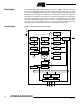
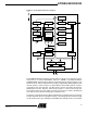


Table Of Contents
- Features
- Description
- Architectural Overview
- General-purpose Register File
- ALU – Arithmetic Logic Unit
- In-System Programmable Flash Program Memory
- EEPROM Data Memory
- SRAM Data Memory
- Program and Data Addressing Modes
- Register Direct, Single Register Rd
- Register Direct, Two Registers Rd and Rr
- I/O Direct
- Data Direct
- Data Indirect with Displacement
- Data Indirect
- Data Indirect with Pre- decrement
- Data Indirect with Post- increment
- Constant Addressing Using the LPM Instruction
- Indirect Program Addressing, IJMP and ICALL
- Relative Program Addressing, RJMP and RCALL
- Memory Access and Instruction Execution Timing
- I/O Memory
- Reset and Interrupt Handling
- Reset Sources
- Power-on Reset
- External Reset
- Watchdog Reset
- MCU Status Register – MCUSR
- Interrupt Handling
- General Interrupt Mask Register – GIMSK
- General Interrupt Flag Register – GIFR
- Timer/Counter Interrupt Mask Register – TIMSK
- Timer/Counter Interrupt FLAG Register – TIFR
- External Interrupt
- Interrupt Response Time
- MCU Control Register – MCUCR
- Sleep Modes
- Timer/Counter
- Watchdog Timer
- EEPROM Read/Write Access
- I/O Port B
- Memory Programming
- Electrical Characteristics
- Typical Characteristics
- AT90S2323/2343 Register Summary
- Ordering Information
- Packaging Information

3
AT90S/LS2323/2343
1004D–09/01
Figure 2. The AT90S/LS2323 Block Diagram
The AT90S2323/2343 provides the following features: 2K bytes of In-System Program-
mable Flash, 128 bytes EEPROM, 128 bytes SRAM, 3 (AT90S/LS2323)/5
(AT90S/LS2343) general-purpose I/O lines, 32 general-purpose working registers, an 8-
bit timer/counter, internal and external interrupts, programmable Watchdog Timer with
internal oscillator, an SPI serial port for Flash Memory downloading and two software-
selectable power-saving modes. The Idle mode stops the CPU while allowing the
SRAM, timer/counters, SPI port and interrupt system to continue functioning. The
Power-down mode saves the register contents but freezes the oscillator, disabling all
other chip functions until the next interrupt or hardware reset.
The device is manufactured using Atmel’s high-density nonvolatile memory technology.
The On-chip Flash allows the program memory to be reprogrammed in-system through
an SPI serial interface. By combining an 8-bit RISC CPU with ISP Flash on a monolithic
PROGRAM
COUNTER
INTERNAL
OSCILLATOR
WATCHDOG
TIMER
STACK
POINTER
PROGRAM
FLASH
MCU CONTROL
REGISTER
SRAM
GENERAL
PURPOSE
REGISTERS
INSTRUCTION
REGISTER
TIMER/
COUNTER
INSTRUCTION
DECODER
DATA DIR.
REG. PORTB
DATA REGISTER
PORTB
PROGRAMMING
LOGIC
TIMING AND
CONTROL
OSCILLATOR
INTERRUPT
UNIT
EEPROM
SPI
STATUS
REGISTER
Z
Y
X
ALU
PORTB DRIVERS
PB0 - PB2
RESET
VCC
GND
CONTROL
LINES
8-BIT DATA BUS