
Manual


Table Of Contents
- Features
- Description
- Architectural Overview
- General-purpose Register File
- ALU – Arithmetic Logic Unit
- In-System Programmable Flash Program Memory
- EEPROM Data Memory
- SRAM Data Memory
- Program and Data Addressing Modes
- Register Direct, Single Register Rd
- Register Direct, Two Registers Rd and Rr
- I/O Direct
- Data Direct
- Data Indirect with Displacement
- Data Indirect
- Data Indirect with Pre- decrement
- Data Indirect with Post- increment
- Constant Addressing Using the LPM Instruction
- Indirect Program Addressing, IJMP and ICALL
- Relative Program Addressing, RJMP and RCALL
- Memory Access and Instruction Execution Timing
- I/O Memory
- Reset and Interrupt Handling
- Reset Sources
- Power-on Reset
- External Reset
- Watchdog Reset
- MCU Status Register – MCUSR
- Interrupt Handling
- General Interrupt Mask Register – GIMSK
- General Interrupt Flag Register – GIFR
- Timer/Counter Interrupt Mask Register – TIMSK
- Timer/Counter Interrupt FLAG Register – TIFR
- External Interrupt
- Interrupt Response Time
- MCU Control Register – MCUCR
- Sleep Modes
- Timer/Counter
- Watchdog Timer
- EEPROM Read/Write Access
- I/O Port B
- Memory Programming
- Electrical Characteristics
- Typical Characteristics
- AT90S2323/2343 Register Summary
- Ordering Information
- Packaging Information
37
AT90S/LS2323/2343
1004D–09/01
Memory Programming
Program and Data
Memory Lock Bits
The AT90S2323/2343 MCU provides two Lock bits that can be left unprogrammed (“1”)
or can be programmed (“0”) to obtain the additional features listed in Table 14. The Lock
bits can only be erased with the Chip Erase operation.
Note: 1. In the high-voltage Serial Programming mode, further programming of the Fuse bits
are also disabled. Program the Fuse bits before programming the Lock bits.
Fuse Bits in
AT90S/LS2323
The AT90S/LS2323 has two Fuse bits, SPIEN and FSTRT.
• When the SPIEN Fuse is programmed (“0”), Serial Program and Data Downloading
are enabled. Default value is programmed (“0”). This bit is not accessible in the low-
voltage Serial Programming mode.
• When the FSTRT Fuse is programmed (“0”), the shortest start-up time is selected
as indicated in Table 6 on page 21. Default value is programmed (“0”). Changing the
FSTRT Fuse does not take effect until the next Power-on Reset. In AT90S/LS2343
the start-up time is fixed.
The status of the Fuse bits is not affected by Chip Erase.
Fuse Bits in
AT90S/LS2343
The AT90S/LS2343 has two Fuse bits, SPIEN and RCEN.
• When the SPIEN Fuse is programmed (“0”), Serial Program and Data Downloading
are enabled. Default value is programmed (“0”). This bit is not accessible in the low-
voltage Serial Programming mode.
• When the RCEN Fuse is programmed (“0”), the internal RC oscillator is selected as
the MCU clock source. Default value is programmed ("0") in AT90LS2343-1. Default
value is un-programmed ("1") in AT90LS2343-4 and AT90S2343-10. Changing the
RCEN Fuse does not take effect until the next Power-on Reset. AT90S/LS2323
cannot select the internal RC oscillator as the MCU source.
The status of the Fuse bits is not affected by Chip Erase.
Signature Bytes All Atmel microcontrollers have a three-byte signature code that identifies the device.
The three bytes reside in a separate address space.
For the AT90S/LS2323
(Note:)
, they are:
1. $000: $1E (indicates manufactured by Atmel)
2. $001: $91 (indicates 2K bytes Flash memory)
3. $002: $02 (indicates AT90S/LS2323 when signature byte $001 is $91)
For AT90S/LS2343
(Note:)
, they are:
1. $000: $1E (indicates manufactured by Atmel)
2. $001: $91 (indicates 2K bytes Flash memory)
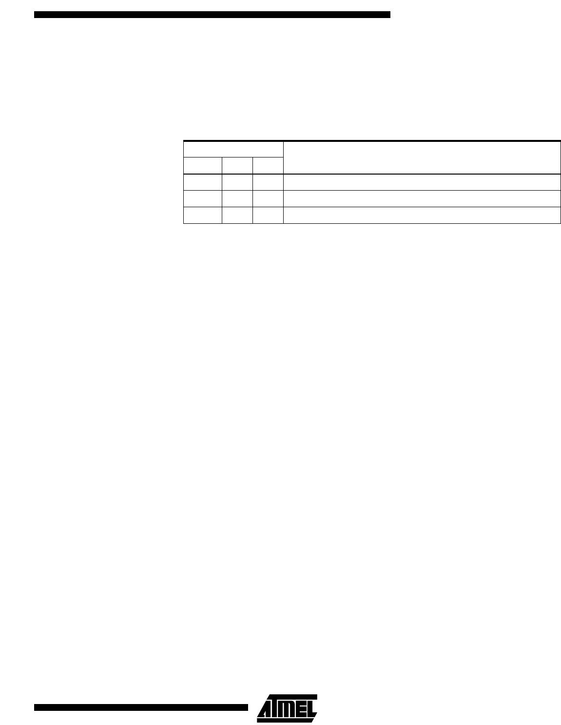
Table 14. Lock Bit Protection Modes
Memory Lock Bits
Protection TypeMode LB1 LB2
1 1 1 No memory lock features enabled.
2 0 1 Further programming of the Flash and EEPROM is disabled.
(1)
3 0 0 Same as mode 2, and verify is also disabled.