
Manual
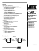
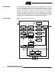
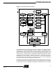
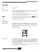


Table Of Contents
- Features
- Description
- Architectural Overview
- General-purpose Register File
- ALU – Arithmetic Logic Unit
- In-System Programmable Flash Program Memory
- EEPROM Data Memory
- SRAM Data Memory
- Program and Data Addressing Modes
- Register Direct, Single Register Rd
- Register Direct, Two Registers Rd and Rr
- I/O Direct
- Data Direct
- Data Indirect with Displacement
- Data Indirect
- Data Indirect with Pre- decrement
- Data Indirect with Post- increment
- Constant Addressing Using the LPM Instruction
- Indirect Program Addressing, IJMP and ICALL
- Relative Program Addressing, RJMP and RCALL
- Memory Access and Instruction Execution Timing
- I/O Memory
- Reset and Interrupt Handling
- Reset Sources
- Power-on Reset
- External Reset
- Watchdog Reset
- MCU Status Register – MCUSR
- Interrupt Handling
- General Interrupt Mask Register – GIMSK
- General Interrupt Flag Register – GIFR
- Timer/Counter Interrupt Mask Register – TIMSK
- Timer/Counter Interrupt FLAG Register – TIFR
- External Interrupt
- Interrupt Response Time
- MCU Control Register – MCUCR
- Sleep Modes
- Timer/Counter
- Watchdog Timer
- EEPROM Read/Write Access
- I/O Port B
- Memory Programming
- Electrical Characteristics
- Typical Characteristics
- AT90S2323/2343 Register Summary
- Ordering Information
- Packaging Information

5
AT90S/LS2323/2343
1004D–09/01
Pin Descriptions
AT90S/LS2343
VCC Supply voltage pin.
GND Ground pin.
Port B (PB4..PB0) Port B is a 5-bit bi-directional I/O port with internal pull-up resistors. The Port B output
buffers can sink 20 mA. As inputs, Port B pins that are externally pulled low, will source
current if the pull-up resistors are activated.
Port B also serves the functions of various special features.
Port pins can provide internal pull-up resistors (selected for each bit). The Port B pins
are tri-stated when a reset condition becomes active.
RESET
Reset input. An external reset is generated by a low level on the RESET pin. Reset
pulses longer than 50 ns will generate a reset, even if the clock is not running. Shorter
pulses are not guaranteed to generate a reset.
CLOCK Clock signal input in external clock mode.
Clock Options
Crystal Oscillator The AT90S/LS2323 contains an inverting amplifier that can be configured for use as an
On-chip oscillator, as shown in Figure 3. XTAL1 and XTAL2 are input and output
respectively. Either a quartz crystal or a ceramic resonator may be used. It is recom-
mended that the AT90S/LS2343 be used if an external clock source is used, since this
gives an extra I/O pin.
Figure 3. Oscillator Connection
External Clock The AT90S/LS2343 can be clocked by an external clock signal, as shown in Figure 4, or
by the On-chip RC oscillator. This RC oscillator runs at a nominal frequency of 1 MHz
(V
CC
= 5V). A fuse bit (RCEN) in the Flash memory selects the On-chip RC oscillator as
the clock source when programmed (“0”). The AT90S/LS2343 is shipped with this bit
programmed. The AT90S/LS2343 is recommended if an external clock source is used,
because this gives an extra I/O pin.
The AT90S/LS2323 can be clocked by an external clock as well, as shown in Figure 4.
No fuse bit selects the clock source for AT90S/LS2323.