
Manual
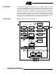
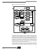
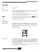


Table Of Contents
- Features
- Description
- Architectural Overview
- General-purpose Register File
- ALU – Arithmetic Logic Unit
- In-System Programmable Flash Program Memory
- EEPROM Data Memory
- SRAM Data Memory
- Program and Data Addressing Modes
- Register Direct, Single Register Rd
- Register Direct, Two Registers Rd and Rr
- I/O Direct
- Data Direct
- Data Indirect with Displacement
- Data Indirect
- Data Indirect with Pre- decrement
- Data Indirect with Post- increment
- Constant Addressing Using the LPM Instruction
- Indirect Program Addressing, IJMP and ICALL
- Relative Program Addressing, RJMP and RCALL
- Memory Access and Instruction Execution Timing
- I/O Memory
- Reset and Interrupt Handling
- Reset Sources
- Power-on Reset
- External Reset
- Watchdog Reset
- MCU Status Register – MCUSR
- Interrupt Handling
- General Interrupt Mask Register – GIMSK
- General Interrupt Flag Register – GIFR
- Timer/Counter Interrupt Mask Register – TIMSK
- Timer/Counter Interrupt FLAG Register – TIFR
- External Interrupt
- Interrupt Response Time
- MCU Control Register – MCUCR
- Sleep Modes
- Timer/Counter
- Watchdog Timer
- EEPROM Read/Write Access
- I/O Port B
- Memory Programming
- Electrical Characteristics
- Typical Characteristics
- AT90S2323/2343 Register Summary
- Ordering Information
- Packaging Information

9
AT90S/LS2323/2343
1004D–09/01
General-purpose
Register File
Figure 7 shows the structure of the 32 general-purpose registers in the CPU.
Figure 7. AVR
CPU General-purpose Working Registers
All the register operating instructions in the instruction set have direct and single-cycle
access to all registers. The only exception is the five constant arithmetic and logic
instructions SBCI, SUBI, CPI, ANDI and ORI between a constant and a register and the
LDI instruction for load immediate constant data. These instructions apply to the second
half of the registers in the register file (R16..R31). The general SBC, SUB, CP, AND and
OR and all other operations between two registers or on a single register apply to the
entire register file.
As shown in Figure 7, each register is also assigned a data memory address, mapping
them directly into the first 32 locations of the user Data Space. Although the register file
is not physically implemented as SRAM locations, this memory organization provides
great flexibility in access of the registers, as the X-, Y-, and Z-registers can be set to
index any register in the file.
70Addr.
R0 $00
R1 $01
R2 $02
…
R13 $0D
General R14 $0E
Purpose R15 $0F
Working R16 $10
Registers R17 $11
…
R26 $1A X-register low byte
R27 $1B X-register high byte
R28 $1C Y-register low byte
R29 $1D Y-register high byte
R30 $1E Z-register low byte
R31 $1F Z-register high byte