Features • AVR® – High-performance and Low-power RISC Architecture • • • • • • • – 118 Powerful Instructions – Most Single Clock Cycle Execution – 32 x 8 General-purpose Working Registers – Up to 8 MIPS Throughput at 8 MHz Data and Nonvolatile Program Memories – 8K Bytes of In-System Programmable Flash SPI Serial Interface for In-System Programming Endurance: 1,000 Write/Erase Cycles – 512 Bytes EEPROM Endurance: 100,000 Write/Erase Cycles – 512 Bytes Internal SRAM – Programming Lock for Software Secu
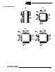
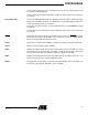
Pin Configurations 2 AT90S/LS8535 1041H–11/01
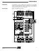
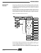
AT90S/LS8535 Description The AT90S8535 is a low-power CMOS 8-bit microcontroller based on the AVR RISC architecture. By executing powerful instructions in a single clock cycle, the AT90S8535 achieves throughputs approaching 1 MIPS per MHz allowing the system designer to optimize power consumption versus processing speed. Block Diagram Figure 1. The AT90S8535 Block Diagram PA0 - PA7 PC0 - PC7 PORTA DRIVERS PORTC DRIVERS VCC GND DATA DIR. REG. PORTA DATA REGISTER PORTA DATA REGISTER PORTC DATA DIR.
The AVR core combines a rich instruction set with 32 general-purpose working registers. All the 32 registers are directly connected to the Arithmetic Logic Unit (ALU), allowing two independent registers to be accessed in one single instruction executed in one clock cycle. The resulting architecture is more code efficient while achieving throughputs up to ten times faster than conventional CISC microcontrollers.
AT90S/LS8535 current if the pull-up resistors are activated. Two Port C pins can alternatively be used as oscillator for Timer/Counter2. The Port C pins are tri-stated when a reset condition becomes active, even if the clock is not running. Port D (PD7..PD0) Port D is an 8-bit bi-directional I/O port with internal pull-up resistors. The Port D output buffers can sink 20 mA. As inputs, Port D pins that are externally pulled low will source current if the pull-up resistors are activated.
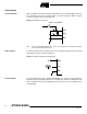
Clock Options Crystal Oscillator XTAL1 and XTAL2 are input and output, respectively, of an inverting amplifier which can be configured for use as an on-chip oscillator, as shown in Figure 2. Either a quartz crystal or a ceramic resonator may be used. Figure 2. Oscillator Connections MAX 1 HC BUFFER HC C2 C1 XTAL2 XTAL1 GND Note: External Clock When using the MCU Oscillator as a clock for an external device, an HC buffer should be connected as indicated in the figure.
AT90S/LS8535 Architectural Overview The fast-access register file concept contains 32 x 8-bit general-purpose working registers with a single clock cycle access time. This means that during one single clock cycle, one Arithmetic Logic Unit (ALU) operation is executed. Two operands are output from the register file, the operation is executed and the result is stored back in the register file – in one clock cycle.
assigned the 32 lowermost Data Space addresses ($00 - $1F), allowing them to be accessed as though they were ordinary memory locations. The I/O memory space contains 64 addresses for CPU peripheral functions as Control Registers, Timer/Counters, A/D converters and other I/O functions. The I/O memory can be accessed directly or as the Data Space locations following those of the register file, $20 - $5F. The AVR uses a Harvard architecture concept – with separate memories and buses for program and data.
AT90S/LS8535 memory. The different interrupts have priority in accordance with their interrupt vector position. The lower the interrupt vector address, the higher the priority. General-purpose Register File Figure 6 shows the structure of the 32 general-purpose working registers in the CPU. Figure 6. AVR CPU General-purpose Working Registers 7 0 Addr.
X-register, Y-register and Zregister The registers R26..R31 have some added functions to their general-purpose usage. These registers are address pointers for indirect addressing of the Data Space. The three indirect address registers, X, Y, and Z, are defined in Figure 7. Figure 7.
AT90S/LS8535 SRAM Data Memory Figure 8 shows how the AT90S8535 SRAM memory is organized. Figure 8. SRAM Organization Register File Data Address Space R0 R1 R2 ... $0000 $0001 $0002 ... R29 R30 R31 I/O Registers $00 $01 $02 ... $001D $001E $001F $3D $3E $3F $005D $005E $005F Internal SRAM $0060 $0061 ... $0020 $0021 $0022 ... $025E $025F The lower 608 data memory locations address the Register file, the I/O memory and the internal data SRAM.
Program and Data Addressing Modes The AT90S8535 AVR RISC microcontroller supports powerful and efficient addressing modes for access to the program memory (Flash) and data memory (SRAM, register file and I/O memory). This section describes the different addressing modes supported by the AVR architecture. In the figures, OP means the operation code part of the instruction word. To simplify, not all figures show the exact location of the addressing bits. Register Direct, Single Register Rd Figure 9.
AT90S/LS8535 Data Direct Figure 12. Direct Data Addressing Data Space 20 19 31 OP $0000 16 Rr/Rd 16 LSBs 15 0 $025F A 16-bit data address is contained in the 16 LSBs of a 2-word instruction. Rd/Rr specify the destination or source register. Data Indirect with Displacement Figure 13.
Data Indirect with Predecrement Figure 15. Data Indirect Addressing with Pre-decrement Data Space $0000 15 0 X, Y OR Z - REGISTER -1 $025F The X-, Y-, or the Z-register is decremented before the operation. Operand address is the decremented contents of the X-, Y-, or the Z-register. Data Indirect with Postincrement Figure 16. Data Indirect Addressing with Post-increment Data Space $0000 15 0 X, Y OR Z - REGISTER 1 $025F The X-, Y-, or the Z-register is incremented after the operation.
AT90S/LS8535 Indirect Program Addressing, IJMP and ICALL Figure 18. Indirect Program Memory Addressing $FFF Program execution continues at address contained by the Z-register (i.e., the PC is loaded with the contents of the Z-register). Relative Program Addressing, RJMP and RCALL Figure 19. Relative Program Memory Addressing +1 $FFF Program execution continues at address PC + k + 1. The relative address k is from 2048 to 2047.
Figure 20. The Parallel Instruction Fetches and Instruction Executions T1 T2 T3 T4 System Clock Ø 1st Instruction Fetch 1st Instruction Execute 2nd Instruction Fetch 2nd Instruction Execute 3rd Instruction Fetch 3rd Instruction Execute 4th Instruction Fetch Figure 21 shows the internal timing concept for the register file. In a single clock cycle an ALU operation using two register operands is executed and the result is stored back to the destination register. Figure 21.
AT90S/LS8535 I/O Memory The I/O space definition of the AT90S8535 is shown in Table 1. Table 1.
Table 1.
AT90S/LS8535 Status Register – SREG The AVR Status Register (SREG) at I/O space location $3F ($5F) is defined as: Bit 7 6 5 4 3 2 1 0 $3F ($5F) I T H S V N Z C Read/Write R/W R/W R/W R/W R/W R/W R/W R/W Initial Value 0 0 0 0 0 0 0 0 SREG • Bit 7 – I: Global Interrupt Enable The global interrupt enable bit must be set (one) for the interrupts to be enabled. The individual interrupt enable control is then performed in separate control registers.
Stack Pointer – SP The AT90S8535 Stack Pointer is implemented as two 8-bit registers in the I/O space locations $3E ($5E) and $3D ($5D). As the AT90S8535 data memory has $25F locations, 10 bits are used.
AT90S/LS8535 Table 2. Reset and Interrupt Vectors (Continued) Vector No.
placed at these locations. The circuit diagram in Figure 23 shows the reset logic. Table 3 defines the timing and electrical parameters of the reset circuitry. Figure 23. Reset Logic Table 3. Reset Characteristics (VCC = 5.0V) Symbol VPOT(1) Parameter Min Typ Max Units Power-on Reset Threshold (rising) 1.0 1.4 1.8 V Power-on Reset Threshold (falling) 0.4 0.6 0.8 V VRST RESET Pin Threshold Voltage tTOUT Reset Delay Time-out Period FSTRT Unprogrammed 11.0 16.0 21.
AT90S/LS8535 Figure 24. MCU Start-up, RESET Tied to VCC. VCC RESET VPOT VRST tTOUT TIME-OUT INTERNAL RESET Figure 25. MCU Start-up, RESET Controlled Externally VCC RESET VPOT VRST TIME-OUT tTOUT INTERNAL RESET External Reset An external reset is generated by a low level on the RESET pin. Reset pulses longer than 50 ns will generate a reset, even if the clock is not running. Shorter pulses are not guaranteed to generate a reset.
Watchdog Reset When the Watchdog times out, it will generate a short reset pulse of 1 XTAL cycle duration. On the falling edge of this pulse, the delay timer starts counting the Time-out period tTOUT. Refer to page 49 for details on operation of the Watchdog. Figure 27. Watchdog Reset during Operation MCU Status Register – MCUSR The MCU Status Register provides information on which reset source caused an MCU reset.
AT90S/LS8535 Table 6. Reset Source Identification Interrupt Handling EXTRF PORF Reset Source 0 0 Watchdog Reset 0 1 Power-on Reset 1 0 External Reset 1 1 Power-on Reset The AT90S8535 has two 8-bit interrupt mask control registers: GIMSK (General Interrupt Mask register) and TIMSK (Timer/Counter Interrupt Mask register). When an interrupt occurs, the Global Interrupt Enable I-bit is cleared (zero) and all interrupts are disabled.
sponding interrupt of External Interrupt Request 0 is executed from program memory address $001. See also “External Interrupts.” • Bits 5.0 – Res: Reserved Bits These bits are reserved bits in the AT90S8535 and always read as zero.
AT90S/LS8535 • Bit 5 – TICIE1: Timer/Counter1 Input Capture Interrupt Enable When the TICIE1 bit is set (one) and the I-bit in the Status Register is set (one), the Timer/Counter1 Input Capture Event Interrupt is enabled. The corresponding interrupt (at vector $005) is executed if a capture-triggering event occurs on pin 20, PD6 (ICP) (i.e., when the ICF1 bit is set in the Timer/Counter Interrupt Flag Register [TIFR]).
• Bit 5 – ICF1: Input Capture Flag 1 The ICF1 bit is set (one) to flag an input capture event, indicating that the Timer/Counter1 value has been transferred to the Input Capture Register (ICR1). ICF1 is cleared by hardware when executing the corresponding interrupt handling vector. Alternatively, ICF1 is cleared by writing a logical “1” to the flag. When the SREG I-bit and TICIE1 (Timer/Counter1 Input Capture Interrupt Enable) and ICF1 are set (one), the Timer/Counter1 Capture Interrupt is executed.
AT90S/LS8535 Interrupt Response Time The interrupt execution response for all the enabled AVR interrupts is four clock cycles minimum. Four clock cycles after the interrupt flag has been set, the program vector address for the actual interrupt handling routine is executed. During this 4-clock-cycle period, the Program Counter (2 bytes) is pushed onto the stack and the Stack Pointer is decremented by 2. The vector is normally a relative jump to the interrupt routine and this jump takes two clock cycles.
Table 8. Interrupt 1 Sense Control ISC11 ISC10 Description 0 0 The low level of INT1 generates an interrupt request. 0 1 Reserved 1 0 The falling edge of INT1 generates an interrupt request. 1 1 The rising edge of INT1 generates an interrupt request. The value on the INT pin is sampled before detecting edges. If edge interrupt is selected, pulses that last longer than one CPU clock period will generate an interrupt. Shorter pulses are not guaranteed to generate an interrupt.
AT90S/LS8535 Comparator Interrupt is not required, the Analog Comparator can be powered down by setting the ACD-bit in the Analog Comparator Control and Status Register (ACSR). This will reduce power consumption in Idle Mode. When the MCU wakes up from Idle Mode, the CPU starts program execution immediately. Power-down Mode When the SM1/SM0 bits are set to 10, the SLEEP instruction makes the MCU enter the Power-down mode.
Timer/Counters The AT90S8535 provides three general-purpose Timer/Counters – two 8-bit T/Cs and one 16-bit T/C. Timer/Counter2 can optionally be asynchronously clocked from an external oscillator. This oscillator is optimized for use with a 32.768 kHz watch crystal, enabling use of Timer/Counter2 as a Real-time Clock (RTC). Timer/Counters 0 and 1 have individual prescaling selection from the same 10-bit prescaling timer. Timer/Counter2 has its own prescaler.
AT90S/LS8535 The clock source for Timer/Counter2 prescaler is named PCK2. PCK2 is by default connected to the main system clock (CK). By setting the AS2 bit in ASSR, Timer/Counter2 prescaler is asynchronously clocked from the PC6(TOSC1) pin. This enables use of Timer/Counter2 as a Real-time Clock (RTC). When AS2 is set, pins PC6(TOSC1) and PC7(TOSC2) are disconnected from Port C.
Timer/Counter0 Control Register – TCCR0 Bit 7 6 5 4 3 2 1 0 $33 ($53) – – – – – CS02 CS01 CS00 Read/Write R R R R R R/W R/W R/W Initial Value 0 0 0 0 0 0 0 0 TCCR0 • Bits 7..3 – Res: Reserved Bits These bits are reserved bits in the AT90S8535 and always read zero. • Bits 2, 1, 0 – CS02, CS01, CS00: Clock Select0, Bits 2, 1 and 0 The Clock Select0 bits 2,1 and 0 define the prescaling source of Timer/Counter0. Table 10.
AT90S/LS8535 16-bit Timer/Counter1 Figure 31 shows the block diagram for Timer/Counter1. Figure 31. Timer/Counter1 Block Diagram TOV0 8 7 CS11 CS10 CS12 CTC1 ICNC1 ICES1 PWM11 T/C1 CONTROL REGISTER B (TCCR1B) PWM10 COM1B1 COM1B0 COM1A1 TOV1 OCF1A OCF1B T/C1 CONTROL REGISTER A (TCCR1A) COM1A0 OCF1A TOV1 ICF1 T/C1 COMPARE T/C1 INPUT MATCHB IRQ CAPTURE IRQ TIMER INT.
the counter on compareA match and actions on the Output Compare pins on both compare matches. Timer/Counter1 can also be used as an 8-, 9- or 10-bit Pulse Width Modulator. In this mode the counter and the OCR1A/OCR1B registers serve as a dual glitch-free standalone PWM with centered pulses. Refer to page 40 for a detailed description of this function.
AT90S/LS8535 Table 11. Compare 1 Mode Select COM1X1 COM1X0 0 0 Timer/Counter1 disconnected from output pin OC1X 0 1 Toggle the OC1X output line. 1 0 Clear the OC1X output line (to zero). 1 Set the OC1X output line (to one). 1 Note: Description X = A or B. In PWM mode, these bits have a different function. Refer to Table 15 for a detailed description.
• Bit 3 – CTC1: Clear Timer/Counter1 on Compare Match When the CTC1 control bit is set (one), the Timer/Counter1 is reset to $0000 in the clock cycle after a compareA match. If the CTC1 control bit is cleared, Timer/Counter1 continues counting and is unaffected by a compare match. Since the compare match is detected in the CPU clock cycle following the match, this function will behave differently when a prescaling higher than 1 is used for the timer.
AT90S/LS8535 TEMP, interrupts must be disabled during access from the main program (and from interrupt routines if interrupts are allowed from within interrupt routines). • TCNT1 Timer/Counter1 Write: When the CPU writes to the high byte TCNT1H, the written data is placed in the TEMP register. Next, when the CPU writes the low byte TCNT1L, this byte of data is combined with the byte data in the TEMP register, and all 16 bits are written to the TCNT1 Timer/Counter1 register simultaneously.
OCR1AL or OCR1BL, the TEMP register is simultaneously written to OCR1AH or OCR1BH. Consequently, the high byte OCR1AH or OCR1BH must be written first for a full 16-bit register write operation. The TEMP register is also used when accessing TCNT1 and ICR1. If the main program and interrupt routines perform access to registers using TEMP, interrupts must be disabled during access from the main program.
AT90S/LS8535 up-counting and down-counting values are reached simultaneously. When the prescaler is in use (CS12..CS10 ≠ 001 or 000), the PWM output goes active when the counter reaches TOP value, but the down-counting compare match is not interpreted to be reached before the next time the counter reaches the TOP value, making a one-period PWM pulse. Table 15. Compare1 Mode Select in PWM Mode COM1X1 COM1X0 0 0 Not connected 0 1 Not connected 1 0 Cleared on compare match, up-counting.
Table 16. PWM Outputs OCR1X = $0000 or TOP Note: COM1X1 COM1X0 OCR1X Output OC1X 1 0 TOP H 1 1 $0000 H 1 X=A 1 TOP L In PWM mode, the Timer Overflow Flag1 (TOV1) is set when the counter advances from $0000. Timer Overflow Interrupt1 operates exactly as in normal Timer/Counter mode, i.e., it is executed when TOV1 is set, provided that Timer Overflow Interrupt1 and global interrupts are enabled. This also applies to the Timer Output Compare1 flags and interrupts.
AT90S/LS8535 Timer/Counter Control Register (TCCR2). The interrupt enable/disable settings are found in the Timer/Counter Interrupt Mask Register (TIMSK). This module features a high-resolution and a high-accuracy usage with the lower prescaling opportunities. Similarly, the high prescaling opportunities make this unit useful for lower speed functions or exact timing functions with infrequent actions.
When the prescaler is set to divide by 8, the timer will count like this: ... | C-2, C-2, C-2, C-2, C-2, C-2, C-2, C-2 | C-1, C-1, C-1, C-1, C-1, C-1, C-1, C-1 | C, 0, 0, 0, 0, 0, 0, 0 | 1, 1, 1,... In PWM mode, this bit has no effect. • Bits 2, 1, 0 – CS22, CS21, CS20: Clock Select Bits 2, 1 and 0 The Clock Select bits 2,1 and 0 define the prescaling source of Timer/Counter2. Table 18. Timer/Counter2 Prescale Select CS22 CS21 CS20 Description 0 0 0 Timer/Counter2 is stopped.
AT90S/LS8535 Timer/Counter2 in PWM Mode When the PWM mode is selected, Timer/Counter2 and the Output Compare Register (OCR2) form an 8-bit, free-running, glitch-free and phase correct PWM with outputs on the PD7(OC2) pin. Timer/Counter2 acts as an up/down counter, counting up from $00 to $FF, where it turns and counts down again to zero before the cycle is repeated.
Table 20. PWM Outputs OCR2 = $00 or $FF COM21 COM20 OCR2 Output PWM2 1 0 $FF H 1 1 $00 H 1 1 $FF L In PWM mode, the Timer Overflow Flag (TOV2) is set when the counter advances from $00. Timer Overflow Interrupt2 operates exactly as in normal Timer/Counter mode, i.e., it is executed when TOV2 is set, provided that Timer Overflow Interrupt and global interrupts are enabled. This also applies to the Timer Output Compare flag and interrupt.
AT90S/LS8535 Asynchronous Operation of Timer/Counter2 When Timer/Counter2 operates asynchronously, some considerations must be taken. • Warning: When switching between asynchronous and synchronous clocking of Timer/Counter2, the timer registers TCNT2, OCR2 and TCCR2 might get corrupted. A safe procedure for switching clock source is: 1. Disable the Timer/Counter2 interrupts OCIE2 and TOIE2. 2. Select clock source by setting AS2 as appropriate. 3. Write new values to TCNT2, OCR2 and TCCR2. 4.
least one before the processor can read the counter value. After wake-up, the MCU is halted for four cycles, it executes the interrupt routine, and resumes execution from the instruction following SLEEP. • 48 During asynchronous operation, the synchronization of the interrupt flags for the asynchronous timer takes three processor cycles plus one timer cycle. The timer is therefore advanced by at least 1 before the processor can read the timer value causing the setting of the interrupt flag.
AT90S/LS8535 Watchdog Timer The Watchdog Timer is clocked from a separate On-chip oscillator. By controlling the Watchdog Timer prescaler, the Watchdog reset interval can be adjusted as shown in Table 21. See characterization data for typical values at other VCC levels. The WDR (Watchdog Reset) instruction resets the Watchdog Timer. Eight different clock cycle periods can be selected to determine the reset period.
1. In the same operation, write a logical “1” to WDTOE and WDE. A logical “1” must be written to WDE even though it is set to “1” before the disable operation starts. 2. Within the next four clock cycles, write a logical “0” to WDE. This disables the Watchdog. • Bits 2..0 – WDP2, WDP1, WDP0: Watchdog Timer Prescaler 2, 1 and 0 The WDP2, WDP1 and WDP0 bits determine the Watchdog Timer prescaling when the Watchdog Timer is enabled.
AT90S/LS8535 EEPROM Read/Write Access The EEPROM access registers are accessible in the I/O space. The write access time is in the range of 2.5 - 4 ms, depending on the VCC voltages. A self-timing function lets the user software detect when the next byte can be written. A special EEPROM Ready interrupt can be set to trigger when the EEPROM is ready to accept new data. In order to prevent unintentional EEPROM writes, a specific write procedure must be followed.
• Bit 2 – EEMWE: EEPROM Master Write Enable The EEMWE bit determines whether setting EEWE to “1” causes the EEPROM to be written. When EEMWE is set (one), setting EEWE will write data to the EEPROM at the selected address. If EEMWE is zero, setting EEWE will have no effect. When EEMWE has been set (one) by software, hardware clears the bit to zero after four clock cycles. See the description of the EEWE bit for a EEPROM write procedure.
AT90S/LS8535 Prevent EEPROM Corruption During periods of low VCC, the EEPROM data can be corrupted because the supply voltage is too low for the CPU and the EEPROM to operate properly. These issues are the same as for board level systems using the EEPROM and the same design solutions should be applied. An EEPROM data corruption can be caused by two situations when the voltage is too low. First, a regular write sequence to the EEPROM requires a minimum voltage to operate correctly.
Serial Peripheral Interface – SPI The Serial Peripheral Interface (SPI) allows high-speed synchronous data transfer between the AT90S8535 and peripheral devices or between several AVR devices. The AT90S8535 SPI features include the following: • Full-duplex, 3-wire Synchronous Data Transfer • Master or Slave Operation • LSB First or MSB First Data Transfer • Four Programmable Bit Rates • End-of-transmission Interrupt Flag • Write Collision Flag Protection • Wake-up from Idle Mode Figure 37.
AT90S/LS8535 Figure 38. SPI Master-slave Interconnection MSB MASTER LSB MISO MISO 8 BIT SHIFT REGISTER SPI CLOCK GENERATOR MSB MASTER LSB 8 BIT SHIFT REGISTER MOSI MOSI SCK SCK SS VCC SS The system is single-buffered in the transmit direction and double-buffered in the receive direction. This means that bytes to be transmitted cannot be written to the SPI Data Register before the entire shift cycle is completed.
SS Pin Functionality When the SPI is configured as a master (MSTR in SPCR is set), the user can determine the direction of the SS pin. If SS is configured as an output, the pin is a general output pin, which does not affect the SPI system. If SS is configured as an input, it must be held high to ensure master SPI operation.
AT90S/LS8535 Figure 40. SPI Transfer Format with CPHA = 1 and DORD = 0 SPI Control Register – SPCR Bit 7 6 5 4 3 2 1 0 $0D ($2D) SPIE SPE DORD MSTR CPOL CPHA SPR1 SPR0 Read/Write R/W R/W R/W R/W R/W R/W R/W R/W Initial Value 0 0 0 0 0 0 0 0 SPCR • Bit 7 – SPIE: SPI Interrupt Enable This bit causes the SPI interrupt to be executed if SPIF bit in the SPSR register is set and the global interrupts are enabled.
• Bits 1,0 – SPR1, SPR0: SPI Clock Rate Select 1 and 0 These two bits control the SCK rate of the device configured as a master. SPR1 and SPR0 have no effect on the slave. The relationship between SCK and the oscillator clock frequency fcl is shown in Table 23. Table 23.
AT90S/LS8535 UART The AT90S8535 features a full duplex (separate receive and transmit registers) Universal Asynchronous Receiver and Transmitter (UART).
is selected (the CHR9 bit in the UART Control Register, UCR is set), the TXB8 bit in UCR is transferred to bit 9 in the Transmit shift register. On the baud rate clock following the transfer operation to the shift register, the start bit is shifted out on the TXD pin. Then follows the data, LSB first. When the stop bit has been shifted out, the shift register is loaded if any new data has been written to the UDR during the transmission. During loading, UDRE is set.
AT90S/LS8535 1 denote the first zero-sample. Following the 1-to-0 transition, the receiver samples the RXD pin at samples 8, 9 and 10. If two or more of these three samples are found to be logical “1”s, the start bit is rejected as a noise spike and the receiver starts looking for the next 1-to-0 transition. If however, a valid start bit is detected, sampling of the data bits following the start bit is performed. These bits are also sampled at samples 8, 9 and 10.
UART Control UART I/O Data Register – UDR Bit 7 6 5 4 3 2 1 0 $0C ($2C) MSB LSB Read/Write R/W R/W R/W R/W R/W R/W R/W R/W Initial Value 0 0 0 0 0 0 0 0 UDR The UDR register is actually two physically separate registers sharing the same I/O address. When writing to the register, the UART Transmit Data register is written. When reading from UDR, the UART Receive Data register is read.
AT90S/LS8535 The FE bit is cleared when the stop bit of received data is one. • Bit 3 – OR: OverRun This bit is set if an Overrun condition is detected, i.e., when a character already present in the UDR register is not read before the next character has been shifted into the Receiver Shift register. The OR bit is buffered, which means that it will be set once the valid data still in UDR is read. The OR bit is cleared (zero) when data is received and transferred to UDR. • Bits 2..
Baud Rate Generator The baud rate generator is a frequency divider which generates baud rates according to the following equation: f CK BAUD = ------------------------------------16(UBRR + 1 ) • BAUD = Baud rate • fCK = Crystal clock frequency • UBRR = Contents of the UART Baud Rate register, UBRR (0 - 255) For standard crystal frequencies, the most commonly used baud rates can be generated by using the UBRR settings in Table 24.
AT90S/LS8535 UART Baud Rate Register – UBRR Bit 7 6 5 4 3 2 1 0 $09 ($29) MSB LSB Read/Write R/W R/W R/W R/W R/W R/W R/W R/W Initial Value 0 0 0 0 0 0 0 0 UBRR The UBRR register is an 8-bit read/write register that specifies the UART Baud Rate according to the equation on the previous page.
Analog Comparator The Analog Comparator compares the input values on the positive input PB2 (AIN0) and negative input PB3 (AIN1). When the voltage on the positive input PB2 (AIN0) is higher than the voltage on the negative input PB3 (AIN1), the Analog Comparator Output (ACO) is set (one). The comparator’s output can be set to trigger the Timer/Counter1 Input Capture function. In addition, the comparator can trigger a separate interrupt, exclusive to the Analog Comparator.
AT90S/LS8535 • Bit 2 – ACIC: Analog Comparator Input Capture Enable When set (one), this bit enables the Input Capture function in Timer/Counter1 to be triggered by the Analog Comparator. The comparator output is in this case directly connected to the Input Capture front-end logic, making the comparator utilize the noise canceler and edge select features of the Timer/Counter1 Input Capture interrupt. When cleared (zero), no connection between the Analog Comparator and the Input Capture function is given.
Analog-to-Digital Converter Feature list • • • • • • • • • • 10-bit Resolution 0.5 LSB Integral Non-linearity ±2 LSB Absolute Accuracy 65 - 260 µs Conversion Time Up to 15 kSPS at Maximum Resolution 8 Multiplexed Input Channels Rail-to-Rail Input Range Free Running or Single Conversion Mode Interrupt on ADC Conversion Complete Sleep Mode Noise Canceler The AT90S8535 features a 10-bit successive approximation ADC.
AT90S/LS8535 Operation The ADC converts an analog input voltage to a 10-bit digital value through successive approximation. The minimum value represents AGND and the maximum value represents the voltage on the AREF pin minus one LSB. The analog input channel is selected by writing to the MUX bits in ADMUX. Any of the eight ADC input pins ADC7..0 can be selected as single-ended inputs to the ADC. The ADC can operate in two modes – Single Conversion and Free Running.
higher sampling rate. See “ADC Characteristics” on page 75 for more details. The ADC module contains a prescaler, which divides the system clock to an acceptable ADC clock frequency. The ADPS2..0 bits in ADCSR are used to generate a proper ADC clock input frequency from any CPU frequency above 100 kHz. The prescaler starts counting from the moment the ADC is switched on by setting the ADEN bit in ADCSR.
AT90S/LS8535 Figure 48. ADC Timing Diagram, Single Conversion One Conversion Cycle number 2 1 3 4 5 6 7 8 Next Conversion 10 9 11 12 13 1 2 3 ADC clock ADSC ADIF ADCH Sign and MSB of result ADCL LSB of result Sample & hold Conversion complete MUX and REFS update MUX and REFS update Figure 49.
2. Enter Idle Mode. The ADC will start a conversion once the CPU has been halted. 3. If no other interrupts occur before the ADC conversion completes, the ADC interrupt will wake up the MCU and execute the ADC Conversion Complete Interrupt routine. ADC Multiplexer Select Register – ADMUX Bit 7 6 5 4 3 2 1 0 $07 ($27) – – – – – MUX2 MUX1 MUX0 Read/Write R R R R R R/W R/W R/W Initial Value 0 0 0 0 0 0 0 0 ADMUX • Bits 7..
AT90S/LS8535 ADSC will read as one as long as a conversion is in progress. When the conversion is complete, it returns to zero. When a extended conversion precedes a real conversion, ADSC will stay high until the real conversion completes. Writing a “0” to this bit has no effect. • Bit 5 – ADFR: ADC Free Running Select When this bit is set (one), the ADC operates in Free Running Mode. In this mode, the ADC samples and updates the data registers continuously.
• ADC9..0: ADC Conversion result These bits represent the result from the conversion. $000 represents analog ground and $3FF represents the selected reference voltage minus one LSB. Scanning Multiple Channels Since change of analog channel always is delayed until a conversion is finished, the Free Running Mode can be used to scan multiple channels without interrupting the converter. Typically, the ADC Conversion Complete interrupt will be used to perform the channel shift.
AT90S/LS8535 ADC Characteristics TA = -40°C to 85°C Symbol Parameter Condition Min Typ Resolution Units 10 Bits Absolute accuracy VREF = 4V ADC clock = 200 kHz 1 Absolute accuracy VREF = 4V ADC clock = 1 MHz 4 LSB Absolute accuracy VREF = 4V ADC clock = 2 MHz 16 LSB Integral Non-linearity VREF > 2V 0.5 LSB Differential Non-linearity VREF > 2V 0.
I/O Ports All AVR ports have true read-modify-write functionality when used as general digital I/O ports. This means that the direction of one port pin can be changed without unintentionally changing the direction of any other pin with the SBI and CBI instructions. The same applies for changing drive value (if configured as output) or enabling/disabling of pull-up resistors (if configured as input). Port A Port A is an 8-bit bi-directional I/O port.
AT90S/LS8535 Port A as General Digital I/O All eight pins in Port A have equal functionality when used as digital I/O pins. PAn, general I/O pin: The DDAn bit in the DDRA register selects the direction of this pin. If DDAn is set (one), PAn is configured as an output pin. If DDAn is cleared (zero), PAn is configured as an input pin. If PORTAn is set (one) when the pin is configured as an input pin, the MOS pull-up resistor is activated.
Port B Port B is an 8-bit bi-directional I/O port. Three I/O memory address locations are allocated for the Port B, one each for the Data Register – PORTB, $18($38), Data Direction Register – DDRB, $17($37) and the Port B Input Pins – PINB, $16($36). The Port B Input Pins address is read-only, while the Data Register and the Data Direction Register are read/write. All port pins have individually selectable pull-up resistors. The Port B output buffers can sink 20 mA and thus drive LED displays directly.
AT90S/LS8535 Port B As General Digital I/O All eight pins in Port B have equal functionality when used as digital I/O pins. PBn, general I/O pin: The DDBn bit in the DDRB register selects the direction of this pin. If DDBn is set (one), PBn is configured as an output pin. If DDBn is cleared (zero), PBn is configured as an input pin. If PORTBn is set (one) when the pin is configured as an input pin, the MOS pull-up resistor is activated.
allows analog signals that are close to VCC/2 to be present during power-down without causing excessive power consumption. • AIN0 – Port B, Bit 2 AIN0, Analog Comparator Positive Input. When configured as an input (DDB2 is cleared [zero]) and with the internal MOS pull-up resistor switched off (PB2 is cleared [zero]), this pin also serves as the positive input of the on-chip Analog Comparator. During Power-down mode, the Schmitt trigger of the digital input is disconnected.
AT90S/LS8535 Figure 53. Port B Schematic Diagram (Pins PB2 and PB3) RD MOS PULLUP RESET Q D DDBn WD RESET Q D PORTBn C PBn RL PWRDN WP RP TO COMPARATOR WP: WD: RL: RP: RD: n: m: DATA BUS C AINm WRITE PORTB WRITE DDRB READ PORTB LATCH READ PORTB PIN READ DDRB 2, 3 0, 1 Figure 54.
Figure 55. Port B Schematic Diagram (Pin PB5) RD MOS PULLUP RESET Q R D DDB5 WD RESET R Q D PORTB5 PB5 DATA BUS C C RL WP RP WP: WD: RL: RP: RD: SPE: MSTR WRITE PORTB WRITE DDRB READ PORTB LATCH READ PORTB PIN READ DDRB SPI ENABLE MASTER SELECT MSTR SPE SPI MASTER OUT SPI SLAVE IN Figure 56.
AT90S/LS8535 Figure 57.
Port C Port C is an 8-bit bi-directional I/O port. Three I/O memory address locations are allocated for the Port C, one each for the Data Register – PORTC, $15($35), Data Direction Register – DDRC, $14($34) and the Port C Input Pins – PINC, $13($33). The Port C Input Pins address is read-only, while the Data Register and the Data Direction Register are read/write. All port pins have individually selectable pull-up resistors. The Port C output buffers can sink 20 mA and thus drive LED displays directly.
AT90S/LS8535 Alternate Functions of Port C When the AS2 bit in ASSR is set (one) to enable asynchronous clocking of Timer/Counter2, pins PC6 and PC7 are disconnected from the port. In this mode, a crystal oscillator is connected to the pins and the pins cannot be used as I/O pins. Port C Schematics Note that all port pins are synchronized. The synchronization latch is, however, not shown in the figure. Figure 58.
Figure 60. Port C Schematic Diagram (Pins PC7) Port D Port D is an 8-bit bi-directional I/O port with internal pull-up resistors. Three I/O memory address locations are allocated for Port D, one each for the Data Register – PORTD, $12($32), Data Direction Register – DDRD, $11($31) and the Port D Input Pins – PIND, $10($30). The Port D Input Pins address is read-only, while the Data Register and the Data Direction Register are read/write. The Port D output buffers can sink 20 mA.
AT90S/LS8535 Port D Data Register – PORTD Bit 7 6 5 4 3 2 1 0 PORTD7 PORTD6 PORTD5 PORTD4 PORTD3 PORTD2 PORTD1 PORTD0 Read/Write R/W R/W R/W R/W R/W R/W R/W R/W Initial Value 0 0 0 0 0 0 0 0 $12 ($32) Port D Data Direction Register – DDRD Bit 7 6 5 4 3 2 1 0 DDD7 DDD6 DDD5 DDD4 DDD3 DDD2 DDD1 DDD0 Read/Write R/W R/W R/W R/W R/W R/W R/W R/W Initial Value 0 0 0 0 0 0 0 0 $11 ($31) Port D Input Pins Address – PIND Bit 7 6 5 4 3 2
• OC1A – Port D, Bit 5 OC1A, Output compare matchA output: The PD5 pin can serve as an external output for the Timer/Counter1 output compareA. The pin has to be configured as an output (DDD5 set [one]) to serve this function. See the timer description on how to enable this function. The OC1A pin is also the output pin for the PWM mode timer function. • OC1B – Port D, Bit 4 OC1B, Output compare matchB output: The PD4 pin can serve as an external output for the Timer/Counter1 output compareB.
AT90S/LS8535 Port D Schematics Note that all port pins are synchronized. The synchronization latches are, however, not shown in the figures. Figure 61. Port D Schematic Diagram (Pin PD0) RD MOS PULLUP RESET Q D DDD0 C DATA BUS WD RESET Q D PORTD0 C PD0 RL WP RP WP: WD: RL: RP: RD: RXD: RXEN: RXEN WRITE PORTD WRITE DDRD READ PORTD LATCH READ PORTD PIN READ DDRD UART RECEIVE DATA UART RECEIVE ENABLE RXD Figure 62.
Figure 63. Port D Schematic Diagram (Pins PD2 and PD3) Figure 64.
AT90S/LS8535 Figure 65. Port D Schematic Diagram (Pin PD6) RD MOS PULLUP RESET Q R D DDD6 WD RESET R Q D PORTD6 PD6 DATA BUS C C RL WP RP WP: WD: RL: RP: RD: ACIC: ACO: WRITE PORTD WRITE DDRD READ PORTD LATCH READ PORTD PIN READ DDRD COMPARATOR IC ENABLE COMPARATOR OUTPUT 0 NOISE CANCELER EDGE SELECT ICNC1 ICES1 ICF1 1 ACIC ACO Figure 66.
Memory Programming Program and Data Memory Lock Bits The AT90S8535 MCU provides two Lock bits that can be left unprogrammed (“1”) or can be programmed (“0”) to obtain the additional features listed in Table 35. The Lock bits can only be erased with the Chip Erase command. Table 35. Lock Bit Protection Modes Memory Lock Bits Mode LB1 LB2 1 1 1 No memory lock features enabled. 2 0 1 Further programming of the Flash and EEPROM is disabled.(1) 3 0 0 Same as mode 2 and verify is also disabled.
AT90S/LS8535 Table 36. Supply Voltage during Programming Part Serial Programming Parallel Programming AT90S8535 4.0 - 6.0V 4.5 - 5.5V AT90LS8535 2.7 - 6.0V 4.5 - 5.5V Parallel Programming This section describes how to parallel program and verify Flash program memory, EEPROM data memory, Lock bits and Fuse bits in the AT90S8535. Signal Names In this section, some pins of the AT90S8535 are referenced by signal names describing their function during parallel programming. See Figure 67 and Table 37.
Table 37. Pin Name Mapping Signal Name in Programming Mode Pin Name I/O Function RDY/BSY PD1 O 0: Device is busy programming, 1: Device is ready for new command OE PD2 I Output Enable (Active low) WR PD3 I Write Pulse (Active low) BS PD4 I Byte Select (“0” selects low byte, “1” selects high byte) XA0 PD5 I XTAL Action Bit 0 XA1 PD6 I XTAL Action Bit 1 DATA PB7 - 0 I/O Bi-directional Data Bus (Output when OE is low) Table 38.
AT90S/LS8535 Chip Erase The Chip Erase command will erase the Flash and EEPROM memories and the Lock bits. The Lock bits are not reset until the Flash and EEPROM have been completely erased. The Fuse bits are not changed. Chip Erase must be performed before the Flash or EEPROM is reprogrammed. Load Command “Chip Erase”: 1. Set XA1, XA0 to “10”. This enables command loading. 2. Set BS to “0”. 3. Set DATA to “1000 0000”. This is the command for Chip Erase. 4. Give XTAL1 a positive pulse.
1. Set BS to “1”. This selects high data. 2. Give WR a negative pulse. This starts programming of the data byte. RDY/BSY goes low. 3. Wait until RDY/BSY goes high to program the next byte. (See Figure 69 for signal waveforms.) The loaded command and address are retained in the device during programming. For efficient programming, the following should be considered: • The command needs only be loaded once when writing or reading multiple memory locations.
AT90S/LS8535 Figure 69. Programming the Flash Waveforms (Continued) DATA DATA HIGH XA1 XA0 BS XTAL1 WR RDY/BSY RESET +12V OE Reading the Flash The algorithm for reading the Flash memory is as follows (refer to “Programming the Flash” for details on command and address loading): 1. A: Load Command “0000 0010”. 2. B: Load Address High Byte ($00 - $0F). 3. C: Load Address Low Byte ($00 - $FF). 4. Set OE to “0” and BS to “0”. The Flash word low byte can now be read at DATA. 5. Set BS to “1”.
Programming the Fuse Bits The algorithm for programming the Fuse bits is as follows (refer to “Programming the Flash” for details on command and data loading): 1. A: Load Command “0100 0000”. 2. D: Load Data Low Byte. Bit n = “0” programs and bit n = “1” erases the Fuse bit. Bit 5 = SPIEN Fuse bit. Bit 0 = FSTRT Fuse bit. Bit 7-6,4-1 = “1”. These bits are reserved and should be left unprogrammed (“1”). 3. Give WR a tWLWH_PFB-wide negative pulse to execute the programming, tWLWH_PFB is found in Table 40.
AT90S/LS8535 Parallel Programming Characteristics Figure 70. Parallel Programming Timing tXLWL tXHXL XTAL1 tDVXH tXLDX tBVWL tWLWH WR tRHBX tWHRL Write Data & Contol (DATA, XA0/1, BS) RDY/BSY tXLOL tOHDZ tOLDV DATA Read tWLRH OE Table 40. Parallel Programming Characteristics, TA = 25°C ± 10%, VCC = 5V ± 10% Symbol Parameter Min Typ Max Units VPP Programming Enable Voltage 11.5 12.5 V IPP Programming Enable Current 250.0 µA tDVXH Data and Control Setup before XTAL1 High 67.
Figure 71. Serial Programming and Verify 2.7 - 6.0V AT90S8535 GND RESET VCC PB7 PB6 PB5 CLOCK INPUT SCK MISO MOSI XTAL1 GND For the EEPROM, an auto-erase cycle is provided within the self-timed write instruction and there is no need to first execute the Chip Erase instruction. The Chip Erase instruction turns the content of every memory location in both the program and EEPROM arrays into $FF.
AT90S/LS8535 4. If a Chip Erase is performed (must be done to erase the Flash), wait tWD_ERASE after the instruction, give RESET a positive pulse and start over from step 2. See Table 44 for tWD_ERASE value. 5. The Flash or EEPROM array is programmed one byte at a time by supplying the address and data together with the appropriate Write instruction. An EEPROM memory location is first automatically erased before new data is written.
f Table 42. Serial Programming Instruction Set Instruction Format Instruction Programming Enable Chip Erase Byte 1 Byte 2 Byte 3 Byte4 1010 1100 0101 0011 xxxx xxxx xxxx xxxx Enable serial programming while RESET is low. 1010 1100 100x xxxx xxxx xxxx xxxx xxxx Chip Erase Flash and EEPROM memory arrays. 0010 H000 xxxx aaaa bbbb bbbb oooo oooo Read H (high or low) data o from program memory at word address a:b.
AT90S/LS8535 Serial Programming Characteristics Figure 73. Serial Programming Timing MOSI tOVSH SCK tSHOX tSLSH tSHSL MISO tSLIV Table 43. Serial Programming Characteristics, TA = -40°C to 85°C, VCC = 2.7 - 6.0V (unless otherwise noted) Symbol 1/tCLCL tCLCL 1/tCLCL Parameter Min Oscillator Frequency (VCC = 2.7 - 6.0V) Oscillator Period (VCC = 2.7 - 4.0V) Oscillator Period (VCC = 4.0 - 6.0V) tSHSL 0 Max Units 4.0 MHz 250.0 Oscillator Frequency (VCC = 4.0 - 6.0V) tCLCL Typ ns 0 8.
Electrical Characteristics Absolute Maximum Ratings* Operating Temperature ................................ -40°C to +105°C *NOTICE: Stresses beyond those listed under “Absolute Maximum Ratings” may cause permanent damage to the device. This is a stress rating only and functional operation of the device at these or other conditions beyond those indicated in the operational sections of this specification is not implied.
AT90S/LS8535 DC Characteristics (Continued) TA = -40°C to 85°C, VCC = 2.7V to 6.0V (unless otherwise noted) Symbol Parameter Condition VACIO Analog Comparator Input Offset Voltage VCC = 5V Vin = VCC/2 IACLK Analog Comparator Input Leakage A VCC = 5V Vin = VCC/2 tACPD Analog Comparator Propagation Delay VCC = 2.7V VCC = 4.0V Notes: Min Typ -50.0 750.0 500.0 Max Units 40.0 mV 50.0 nA ns 1. “Max” means the highest value where the pin is guaranteed to be read as low (logical “0”). 2.
External Clock Drive Waveforms Figure 74. External Clock VIH1 VIL1 Table 46. External Clock Drive VCC = 2.7V to 6.0V Symbol 1/tCLCL 106 Parameter Oscillator Frequency VCC = 4.0V to 6.0V Min Max Min Max Units 0 4 0 8.0 MHz tCLCL Clock Period 250.0 125.0 ns tCHCX High Time 100.0 50.0 ns tCLCX Low Time 100.0 50.0 ns tCLCH Rise Time 1.6 0.5 µs tCHCL Fall Time 1.6 0.
AT90S/LS8535 Typical Characteristics The following charts show typical behavior. These figures are not tested during manufacturing. All current consumption measurements are performed with all I/O pins configured as inputs and with internal pull-ups enabled. A sine wave generator with railto-rail output is used as clock source. The power consumption in Power-down mode is independent of clock selection.
Figure 76. Active Supply Current vs. VCC ACTIVE SUPPLY CURRENT vs. Vcc FREQUENCY = 4 MHz 16 14 TA = 25˚C TA = 85˚C I cc(mA) 12 10 8 6 4 2 0 2 2.5 3 3.5 4 4.5 5 5.5 6 Vcc(V) Figure 77. Idle Supply Current vs. Frequency IDLE SUPPLY CURRENT vs. FREQUENCY TA= 25˚C 20 Vcc= 6V 18 Vcc= 5.5V I cc(mA) 16 14 Vcc= 5V 12 Vcc= 4.5V 10 Vcc= 4V Vcc= 3.6V 8 Vcc= 3.3V 6 Vcc= 3.0V 4 Vcc= 2.
AT90S/LS8535 Figure 78. Idle Supply Current vs. VCC IDLE SUPPLY CURRENT vs. Vcc FREQUENCY = 4 MHz 7 6 TA = 85˚C TA = 25˚C I cc(mA) 5 4 3 2 1 0 2 2.5 3 3.5 4 4.5 5 5.5 6 Vcc(V) Figure 79. Power-down Supply Current vs. VCC POWER DOWN SUPPLY CURRENT vs. Vcc WATCHDOG TIMER DISABLED 90 TA = 85˚C 80 I cc(µΑ) 70 60 50 TA = 70˚C 40 30 TA = 45˚C 20 TA = 25˚C 10 0 2 2.5 3 3.5 4 4.5 5 5.
Figure 80. Power-down Supply Current vs. VCC POWER DOWN SUPPLY CURRENT vs. Vcc WATCHDOG TIMER ENABLED 140 120 I cc(µΑ) 100 TA = 85˚C 80 60 40 TA = 25˚C 20 0 2 2.5 3 3.5 4 4.5 5 5.5 6 Vcc(V) Figure 81. Power Save Supply Current vs. VCC POWER SAVE SUPPLY CURRENT vs. Vcc WATCHDOG TIMER DISABLED 90 TA = 85˚C 80 70 I cc(µΑ) 60 50 40 30 TA = 25˚C 20 10 0 2 2.5 3 3.5 4 4.5 5 5.
AT90S/LS8535 Figure 82. Analog Comparator Current vs. VCC ANALOG COMPARATOR CURRENT vs. Vcc 1 0.9 0.8 TA = 25˚C 0.7 TA = 85˚C I cc(mA) 0.6 0.5 0.4 0.3 0.2 0.1 0 2 2.5 3 3.5 4 4.5 5 5.5 6 Vcc(V) Note: Analog comparator offset voltage is measured as absolute offset. Figure 83. Analog Comparator Offset Voltage vs. Common Mode Voltage ANALOG COMPARATOR OFFSET VOLTAGE vs. COMMON MODE VOLTAGE Vcc = 5V 18 16 TA = 25˚C Offset Voltage (mV) 14 12 TA = 85˚C 10 8 6 4 2 0 0 0.5 1 1.5 2 2.5 3 3.
Figure 84. Analog Comparator Offset Voltage vs. Common Mode Voltage ANALOG COMPARATOR OFFSET VOLTAGE vs. COMMON MODE VOLTAGE Vcc = 2.7V 10 TA = 25˚C Offset Voltage (mV) 8 6 TA = 85˚C 4 2 0 0 0.5 1 1.5 2 2.5 3 Common Mode Voltage (V) Figure 85. Analog Comparator Input Leakage Current ANALOG COMPARATOR INPUT LEAKAGE CURRENT VCC = 6V TA = 25˚C 60 50 30 I ACLK (nA) 40 20 10 0 -10 0 0.5 1 1.5 2 2.5 3 3.5 4 4.5 5 5.5 6 6.
AT90S/LS8535 Figure 86. Watchdog Oscillator Frequency vs. VCC WATCHDOG OSCILLATOR FREQUENCY vs. Vcc 1600 TA = 25˚C 1400 TA = 85˚C F RC (KHz) 1200 1000 800 600 400 200 0 2 2.5 3 3.5 4 4.5 5 5.5 6 Vcc (V) Note: Sink and source capabilities of I/O ports are measured on one pin at a time. Figure 87. Pull-up Resistor Current vs. Input Voltage PULL-UP RESISTOR CURRENT vs. INPUT VOLTAGE Vcc = 5V 120 TA = 25˚C 100 TA = 85˚C I OP (µA) 80 60 40 20 0 0 0.5 1 1.5 2 2.5 VOP (V) 3 3.
Figure 88. Pull-up Resistor Current vs. Input Voltage PULL-UP RESISTOR CURRENT vs. INPUT VOLTAGE Vcc = 2.7V 30 TA = 25˚C 25 TA = 85˚C 15 I OP (µA) 20 10 5 0 0 0.5 1 1.5 2 2.5 3 VOP (V) Figure 89. I/O Pin Sink Current vs. Output Voltage I/O PIN SINK CURRENT vs. OUTPUT VOLTAGE Vcc = 5V 70 TA = 25˚C 60 TA = 85˚C 50 30 I OL (mA) 40 20 10 0 0 0.5 1 1.5 2 2.
AT90S/LS8535 Figure 90. I/O Pin Source Current vs. Output Voltage I/O PIN SOURCE CURRENT vs. OUTPUT VOLTAGE Vcc = 5V 20 TA = 25˚C 18 16 TA = 85˚C 14 I OH (mA) 12 10 8 6 4 2 0 0 0.5 1 1.5 2 2.5 3 3.5 4 4.5 5 VOH (V) Figure 91. I/O Pin Sink Current vs. Output Voltage I/O PIN SOURCE CURRENT vs. OUTPUT VOLTAGE Vcc = 2.7V 6 TA = 25˚C 5 TA = 85˚C 3 I OH (mA) 4 2 1 0 0 0.5 1 1.5 2 2.
Figure 92. I/O Pin Source Current vs. Output Voltage I/O PIN SINK CURRENT vs. OUTPUT VOLTAGE Vcc = 2.7V 25 TA = 25˚C 20 TA = 85˚C 10 I OL (mA) 15 5 0 0 0.5 1 1.5 2 VOL (V) Figure 93. I/O Pin Input Threshold Voltage vs. VCC I/O PIN INPUT THRESHOLD VOLTAGE vs. Vcc TA = 25˚C 2.5 Threshold Voltage (V) 2 1.5 1 0.5 0 2.7 4.0 5.
AT90S/LS8535 Figure 94. I/O Pin Input Hysteresis vs. VCC I/O PIN INPUT HYSTERESIS vs. Vcc TA = 25˚C 0.18 0.16 Input hysteresis (V) 0.14 0.12 0.1 0.08 0.06 0.04 0.02 0 2.7 4.0 5.
Register Summary Address Name Bit 7 Bit 6 Bit 5 Bit 4 Bit 3 Bit 2 Bit 1 Bit 0 Page $3F ($5F) SREG I T H S V N Z C page 19 $3E ($5E) SPH - - - - - - SP9 SP8 page 20 $3D ($5D) SPL SP7 SP6 SP5 SP4 SP3 SP2 SP1 SP0 page 20 $3C ($5C) Reserved $3B ($5B) GIMSK INT1 INT0 - - - - - - $3A ($5A) GIFR INTF1 INTF0 $39 ($59) TIMSK OCIE2 TOIE2 TICIE1 OCIE1A OCIE1B TOIE1 - TOIE0 page 26 $38 ($58) TIFR OCF2 TOV2 ICF1 OCF1A OCF1B TOV1 - TOV0 page
AT90S/LS8535 Notes: 1. For compatibility with future devices, reserved bits should be written to zero if accessed. Reserved I/O memory addresses should never be written. 2. Some of the status flags are cleared by writing a logical “1” to them. Note that the CBI and SBI instructions will operate on all bits in the I/O register, writing a one back into any flag read as set, thus clearing the flag. The CBI and SBI instructions work with registers $00 to $1F only.
Instruction Set Summary Mnemonic Operands Description Operation Flags # Clocks ARITHMETIC AND LOGIC INSTRUCTIONS ADD Rd, Rr Add Two Registers Rd ← Rd + Rr Z,C,N,V,H 1 ADC Rd, Rr Add with Carry Two Registers Rd ← Rd + Rr + C Z,C,N,V,H 1 ADIW Rdl, K Add Immediate to Word Rdh:Rdl ← Rdh:Rdl + K Z,C,N,V,S 2 SUB Rd, Rr Subtract Two Registers Rd ← Rd - Rr Z,C,N,V,H 1 SUBI Rd, K Subtract Constant from Register Rd ← Rd - K Z,C,N,V,H 1 SBC Rd, Rr Subtract with Carry Two Registers
AT90S/LS8535 Instruction Set Summary (Continued) Mnemonic Operands Description Operation Flags LD Rd, Y Load Indirect Rd ← (Y) None # Clocks 2 LD Rd, Y+ Load Indirect and Post-inc. Rd ← (Y), Y ← Y + 1 None 2 LD Rd, -Y Load Indirect and Pre-dec. Y ← Y - 1, Rd ← (Y) None 2 LDD Rd, Y+q Load Indirect with Displacement Rd ← (Y + q) None 2 LD Rd, Z Load Indirect Rd ← (Z) None 2 LD Rd, Z+ Load Indirect and Post-inc.
Ordering Information Power Supply Speed (MHz) 2.7 - 6.0V 4 4.0 - 6.
AT90S/LS8535 Packaging Information 44A 44-lead, Thin (1.0mm) Plastic Quad Flat Package (TQFP), 10x10mm body, 2.0mm footprint, 0.8mm pitch. Dimension in Millimeters and (Inches)* JEDEC STANDARD MS-026 ACB 12.25(0.482) SQ 11.75(0.462) PIN 1 ID PIN 1 0.45(0.018) 0.30(0.012) 0.80(0.0315) BSC 10.10(0.394) SQ 9.90(0.386) 1.20(0.047) MAX 0.20(0.008) 0.09(0.004) 0˚~7˚ 0.75(0.030) 0.45(0.018) 0.15(0.006) 0.05(0.002) *Controlling dimension: millimetter REV.
44J 44J, 44-lead, Plastic J-leaded Chip Carrier (PLCC) Dimensions in Milimeters and (Inches)* JEDEC STANDARD MS-018 AC 1.14(0.045) X 45˚ 0.813(0.032) 0.660(0.026) PIN NO. 1 IDENTIFY 1.14(0.045) X 45˚ 16.70(0.656) SQ 16.50(0.650) 17.70(0.695) SQ 17.40(0.685) 1.27(0.050) TYP 12.70(0.500) REF SQ 0.318(0.0125) 0.191(0.0075) 16.00(0.630) SQ 15.00(0.590) 0.533(0.021) 0.330(0.013) 0.50(0.020)MIN 2.11(0.083) 1.57(0.062) 3.05(0.120) 2.29(0.090) 4.57(0.180) 4.19(0.165) 0.51(0.
AT90S/LS8535 40P6 40-lead, Plastic Dual Inline Parkage (PDIP), 0.600" wide Demension in Millimeters and (Inches)* JEDEC STANDARD MS-011 AC 52.71(2.075) 51.94(2.045) PIN 1 13.97(0.550) 13.46(0.530) 48.26(1.900) REF 4.83(0.190)MAX SEATING PLANE 0.38(0.015)MIN 3.56(0.140) 3.05(0.120) 2.54(0.100)BSC 1.65(0.065) 1.27(0.050) 0.56(0.022) 0.38(0.015) 15.88(0.625) 15.24(0.600) 0º ~ 15º REF 0.38(0.015) 0.20(0.008) 17.78(0.700)MAX *Controlling dimension: Inches REV.
44M1 D SEATING PLANE Marked pin#1 identifier E A1 TOP VIEW A3 A L SIDE VIEW PIN #1 CORNER D2 COMMON DIMENSIONS (*Unit of Measure = mm) SYMBOL MIN NOM MAX A 0.80 0.90 1.00 A1 0.00 0.02 0.05 0.25 REF A3 E2 b 0.18 D D2 2.25 e L 0.30 4.70 5.25 7.00 BSC 2.25 e b 0.23 7.00 BSC E E2 NOTE 4.70 5.25 0.50 BSC 0.35 0.55 0.75 BOTTOM VIEW NOTE 1. JEDEC STANDARD MO-220, Fig 1 (Saw Singulation), VKKD-1 07/23/01 R 126 DRAWING NO.
Atmel Headquarters Atmel Product Operations Corporate Headquarters Atmel Colorado Springs 2325 Orchard Parkway San Jose, CA 95131 TEL (408) 441-0311 FAX (408) 487-2600 Europe Atmel SarL Route des Arsenaux 41 Casa Postale 80 CH-1705 Fribourg Switzerland TEL (41) 26-426-5555 FAX (41) 26-426-5500 Asia Atmel Asia, Ltd. Room 1219 Chinachem Golden Plaza 77 Mody Road Tsimhatsui East Kowloon Hong Kong TEL (852) 2721-9778 FAX (852) 2722-1369 Japan Atmel Japan K.K. 9F, Tonetsu Shinkawa Bldg.