
Manual


100
AT90S/LS8535
1041H–11/01
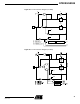
Figure 71. Serial Programming and Verify
For the EEPROM, an auto-erase cycle is provided within the self-timed write instruction
and there is no need to first execute the Chip Erase instruction. The Chip Erase instruc-
tion turns the content of every memory location in both the program and EEPROM
arrays into $FF.
The program and EEPROM memory arrays have separate address spaces: $0000 to
$0FFF for program memory and $0000 to $01FF for EEPROM memory.
Either an external clock is supplied at pin XTAL1 or a crystal needs to be connected
across pins XTAL1 and XTAL2. The minimum low and high periods for the serial clock
(SCK) input are defined as follows:
Low: > 2 XTAL1 clock cycles
High: > 2 XTAL1 clock cycles
Serial Programming
Algorithm
When writing serial data to the AT90S8535, data is clocked on the rising edge of SCK.
When reading data from the AT90S8535, data is clocked on the falling edge of SCK.
See Figure 72, Figure 73 and Table 43 for timing details.
To program and verify the AT90SS8535 in the Serial Programming Mode, the following
sequence is recommended (see 4-byte instruction formats in Table 42
):
1. Power-up sequence:
Apply power between V
CC
and GND while RESET and SCK are set to “0”. If a crys-
tal is not connected across pins XTAL1 and XTAL2, apply a clock signal to the
XTAL1 pin. In some systems, the programmer cannot guarantee that SCK is held
low during power-up. In this case, RESET
must be given a positive pulse of at least
two XTAL1 cycles duration after SCK has been set to “0”.
2. Wait for at least 20 ms and enable serial programming by sending the Program-
ming Enable serial instruction to the MOSI (PB5) pin.
3. The serial programming instructions will not work if the communication is out of
synchronization. When in sync, the second byte ($53) will echo back when issu-
ing the third byte of the Programming Enable instruction. Whether the echo is
correct or not, all four bytes of the instruction must be transmitted. If the $53 did
not echo back, give SCK a positive pulse and issue a new Programming Enable
instruction. If the $53 is not seen within 32 attempts, there is no functional device
connected.
AT90S8535
VCC
2.7 - 6.0V
PB7
PB6
PB5
RESET
GND
XTAL1
SCK
MISO
MOSI
GND
CLOCK INPUT