
Manual


22
AT90S/LS8535
1041H–11/01
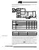
placed at these locations. The circuit diagram in Figure 23 shows the reset logic. Table 3
defines the timing and electrical parameters of the reset circuitry.
Figure 23. Reset Logic
Note: 1. The Power-on Reset will not work unless the supply voltage has been below V
POT
(falling).
Power-on Reset A Power-on Reset (POR) circuit ensures that the device is reset from power-on. As
shown in Figure 23, an internal timer clocked from the Watchdog Timer oscillator pre-
vents the MCU from starting until after a certain period after V
CC
has reached the Power-
on Threshold voltage (V
POT
), regardless of the V
CC
rise time (see Figure 24).
The user can select the start-up time according to typical oscillator start-up time. The
number of WDT oscillator cycles is shown in Table 4. The frequency of the Watchdog
oscillator is voltage-dependent as shown in “Typical Characteristics” on page 107.
If the built-in start-up delay is sufficient, RESET
can be connected to V
CC
directly or via
an external pull-up resistor. By holding the pin low for a period after V
CC
has been
applied, the Power-on Reset period can be extended. Refer to Figure 25 for a timing
example of this.
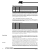
Table 3. Reset Characteristics (V
CC
= 5.0V)
Symbol Parameter Min Typ Max Units
V
POT
(1)
Power-on Reset Threshold (rising) 1.0 1.4 1.8 V
Power-on Reset Threshold (falling) 0.4 0.6 0.8 V
V
RST
RESET Pin Threshold Voltage 0.6 V
CC
V
t
TOUT
Reset Delay Time-out Period
FSTRT Unprogrammed
11.0 16.0 21.0 ms
t
TOUT
Reset Delay Time-out Period
FSTRT Programmed
1.0 1.1 1.2 ms
Table 4. Number of Watchdog Oscillator Cycles
FSTRT Time-out at V
CC
= 5V Number of WDT Cycles
Programmed 1.1 ms 1K
Unprogrammed 16.0 ms 16K