
Manual


29
AT90S/LS8535
1041H–11/01
Interrupt Response Time The interrupt execution response for all the enabled AVR interrupts is four clock cycles
minimum. Four clock cycles after the interrupt flag has been set, the program vector
address for the actual interrupt handling routine is executed. During this 4-clock-cycle
period, the Program Counter (2 bytes) is pushed onto the stack and the Stack Pointer is
decremented by 2. The vector is normally a relative jump to the interrupt routine and this
jump takes two clock cycles. If an interrupt occurs during execution of a multi-cycle
instruction, this instruction is completed before the interrupt is served.
A return from an interrupt handling routine (same as for a subroutine call routine) takes
four clock cycles. During these four clock cycles, the Program Counter (2 bytes) is
popped back from the stack, the Stack Pointer is incremented by 2 and the I-flag in
SREG is set. When the AVR exits from an interrupt, it will always return to the main pro-
gram and execute one more instruction before any pending interrupt is served.
MCU Control Register –
MCUCR
The MCU Control Register contains control bits for general MCU functions.
• Bit 7 – Res: Reserved Bit
This bit is a reserved bit in the AT90S8535 and always reads zero.
• Bit 6 – SE: Sleep Enable
The SE bit must be set (one) to make the MCU enter the Sleep Mode when the SLEEP
instruction is executed. To avoid the MCU entering the Sleep Mode unless it is the pro-
grammer’s purpose, it is recommended to set the Sleep Enable (SE) bit just before the
execution of the SLEEP instruction.
• Bits 5, 4 – SM1/SM0: Sleep Mode Select Bits 1 and 0
These bits select between the three available sleep modes as shown in Table 7.
• Bits 3, 2 – ISC11, ISC10: Interrupt Sense Control 1 Bits 1 and 0
The External Interrupt 1 is activated by the external pin INT1 if the SREG I-flag and the
corresponding interrupt mask in the GIMSK is set. The level and edges on the external
INT1 pin that activate the interrupt are defined in Table 8.
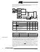
Bit 76543210
$35 ($55) – SE SM1 SM0 ISC11 ISC10 ISC01 ISC00 MCUCR
Read/Write R R/W R/W R/W R/W R/W R/W R/W
Initial Value 0 0 0 0 0 0 0 0
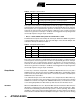
Table 7. Sleep Mode Select
SM1 SM0 Sleep Mode
00Idle
01Reserved
1 0 Power-down
11Power Save