
Manual

7
AT90S/LS8535
1041H–11/01
Architectural
Overview
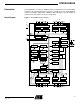
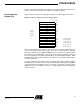
The fast-access register file concept contains 32 x 8-bit general-purpose working regis-
ters with a single clock cycle access time. This means that during one single clock cycle,
one Arithmetic Logic Unit (ALU) operation is executed. Two operands are output from
the register file, the operation is executed and the result is stored back in the register file
– in one clock cycle.
Six of the 32 registers can be used as three 16-bit indirect address register pointers for
Data Space addressing, enabling efficient address calculations. One of the three
address pointers is also used as the address pointer for the constant table look-up func-
tion. These added function registers are the 16-bit X-register, Y-register, and Z-register.
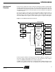
Figure 4. The AT90S8535 AVR RISC Architecture
The ALU supports arithmetic and logic functions between registers or between a con-
stant and a register. Single register operations are also executed in the ALU. Figure 4
shows the AT90S8535 AVR RISC microcontroller architecture.
In addition to the register operation, the conventional memory addressing modes can be
used on the register file as well. This is enabled by the fact that the register file is
4K X 16
Program
Memory
Instruction
Register
Instruction
Decoder
Program
Counter
Control Lines
32 x 8
General
Purpose
Registrers
ALU
Status
and Control
Interrupt
Unit
SPI
Unit
8-bit
Timer/Counter
Watchdog
Timer
Analog to Digital
Converter
Analog
Comparator
32
I/O Lines
512 x 8
EEPROM
Data Bus 8-bit
Serial
UART
16-bit
Timer/Counter
with PWM
8-bit
Timer/Counter
with PWM
512 x 8
Data
SRAM
Direct Addressing
Indirect Addressing