
Manual

9
AT90S/LS8535
1041H–11/01
memory. The different interrupts have priority in accordance with their interrupt vector
position. The lower the interrupt vector address, the higher the priority.
General-purpose
Register File
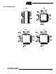
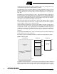
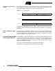
Figure 6 shows the structure of the 32 general-purpose working registers in the CPU.
Figure 6. AVR CPU General-purpose Working Registers
All the register operating instructions in the instruction set have direct and single-cycle
access to all registers. The only exception is the five constant arithmetic and logic
instructions SBCI, SUBI, CPI, ANDI and ORI between a constant and a register and the
LDI instruction for load immediate constant data. These instructions apply to the second
half of the registers in the register file (R16..R31). The general SBC, SUB, CP, AND,
and OR and all other operations between two registers or on a single register apply to
the entire register file.
As shown in Figure 6, each register is also assigned a data memory address, mapping
them directly into the first 32 locations of the user Data Space. Although not being phys-
ically implemented as SRAM locations, this memory organization provides great
flexibility in access of the registers, as the X-, Y-, and Z-registers can be set to index any
register in the file.
70Addr.
R0 $00
R1 $01
R2 $02
…
R13 $0D
General R14 $0E
Purpose R15 $0F
Working R16 $10
Registers R17 $11
…
R26 $1A X-register low byte
R27 $1B X-register high byte
R28 $1C Y-register low byte
R29 $1D Y-register high byte
R30 $1E Z-register low byte
R31 $1F Z-register high byte