
Manual


93
AT90S/LS8535
1041H–11/01
Parallel Programming This section describes how to parallel program and verify Flash program memory,
EEPROM data memory, Lock bits and Fuse bits in the AT90S8535.
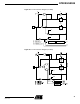
Signal Names In this section, some pins of the AT90S8535 are referenced by signal names describing
their function during parallel programming. See Figure 67 and Table 37. Pins not
described in Table 37 are referenced by pin name.
The XA1/XA0 pins determine the action executed when the XTAL1 pin is given a posi-
tive pulse. The bit coding are shown in Table 38.
When pulsing WR
or OE, the command loaded determines the action executed. The
command is a byte where the different bits are assigned functions as shown in Table 39.
Figure 67. Parallel Programming
Table 36. Supply Voltage during Programming
Part Serial Programming Parallel Programming
AT90S8535 4.0 - 6.0V 4.5 - 5.5V
AT90LS8535 2.7 - 6.0V 4.5 - 5.5V
AT90S8535
VCC
+5V
RESET
GND
XTAL1
PD1
PD2
PD3
PD4
PD5
PD6
+12 V
RDY/BSY
OE
BS
XA0
XA1
WR
PB7 - PB0 DATA