
Manual


99
AT90S/LS8535
1041H–11/01
Parallel Programming
Characteristics
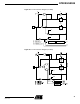
Figure 70. Parallel Programming Timing
Notes: 1. Use t
WLWH_CE
for Chip Erase and t
WLWH_PFB
for programming the Fuse bits.
2. If t
WLWH
is held longer than t
WLRH
, no RDY/BSY pulse will be seen.
Serial Downloading Both the Flash and EEPROM memory arrays can be programmed using the serial SPI
bus while RESET
is pulled to GND. The serial interface consists of pins SCK, MOSI
(input) and MISO (output), see Figure 71. After RESET
is set low, the Programming
Enable instruction needs to be executed first before program/erase operations can be
executed.
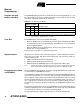
Table 40. Parallel Programming Characteristics, T
A
= 25°C ± 10%, V
CC
= 5V ± 10%
Symbol Parameter Min Typ Max Units
V
PP
Programming Enable Voltage 11.5 12.5 V
I
PP
Programming Enable Current 250.0 µA
t
DVXH
Data and Control Setup before XTAL1 High 67.0 ns
t
XHXL
XTAL1 Pulse Width High 67.0 ns
t
XLDX
Data and Control Hold after XTAL1 Low 67.0 ns
t
XLWL
XTAL1 Low to WR Low 67.0 ns
t
BVWL
BS Valid to WR Low 67.0 ns
t
RHBX
BS Hold after RDY/BSY High 67.0 ns
t
WLWH
WR Pulse Width Low
(1)
67.0 ns
t
WHRL
WR High to RDY/BSY Low
(2)
20.0 ns
t
WLRH
WR Low to RDY/BSY High
(2)
0.5 0.7 0.9 ms
t
XLOL
XTAL1 Low to OE Low 67.0 ns
t
OLDV
OE Low to DATA Valid 20.0 ns
t
OHDZ
OE High to DATA Tri-stated 20.0 ns
t
WLWH_CE
WR Pulse Width Low for Chip Erase 5.0 10.0 15.0 ms
t
WLWH_PFB
WR Pulse Width Low for Programming the
Fuse Bits 1.0 1.5 1.8 ms
Data & Contol
(DATA, XA0/1, BS)
DATA
Write
Read
XTAL1
t
XHXL
t
WLWH
t
DVXH
t
XLOL
t
OLDV
t
WHRL
t
WLRH
WR
RDY/BSY
OE
t
XLDX
t
XLWL
t
RHBX
t
OHDZ
t
BVWL