
Manual

5
6264A–CAP–21-May-07
AT91CAP9S500A/AT91CAP9S250A
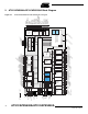
3. Signal Description
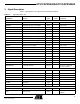
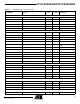
Table 3-1 gives details on the signal name classified by peripheral.
Table 3-1. Signal Description List
Signal Name Function Type
Active
Level Comments
Power Supplies
VDDIOM EBI I/O Lines Power Supply Power 1.65V to 3.6V
VDDIOP0 Peripherals I/O Lines Power Supply Power 3.0V to 3.6V
VDDIOP1 Peripherals I/O Lines Power Supply Power 1.65V to 3.6V
VDDIOMPA MP Block I/O A Lines Power Supply Power 1.65V to 3.6V
VDDIOMPB MP Block I/O B Lines Power Supply Power 1.65V to 3.6V
VDDBU Backup I/O Lines Power Supply Power 1.08V to 1.32V
VDDPLL PLL Power Supply Power 3.0V to 3.6V
VDDUTMII USB UTMI+ Interface Power Supply Power 3.0V to 3.6V
VDDUTMIC USB UTMI+ Core Power Supply Power 1.08V to 1.32V
VDDUPLL USB UTMI+ PLL Power Supply Power 1.08V to 1.32V
VDDANA ADC Analog Power Supply Power 3.0V to 3.6V
VDDCORE Core Chip Power Supply Power 1.08V to 1.32V
GND Ground Ground
GNDPLL PLL Ground Ground
GNDUTMII USB UTMI+ Interface Ground Ground
GNDUTMIC USB UTMI+ Core Ground Ground
GNDUPLL USB UTMI+ PLL Ground Ground
GNDANA ADC Analog Ground Ground
GNDBU Backup Ground Ground
GNDTHERMAL Thermal Ground Ball Ground
Thermally coupled with
package substrate
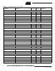
Clocks, Oscillators and PLLs
XIN Main Oscillator Input Input
XOUT Main Oscillator Output Output
XIN32 Slow Clock Oscillator Input Input
XOUT32 Slow Clock Oscillator Output Output
PLLRCA PLL A Filter Input
PLLRCB PLL B Filter Input
PCK0 - PCK3 Programmable Clock Output Output
Shutdown, Wakeup Logic
SHDN Shutdown Control Output Do not tie over VDDBU
WKUP Wake-Up Input Input
Accept between 0V and
VDDBU