
Manual

6
6264A–CAP–21-May-07
AT91CAP9S500A/AT91CAP9S250A
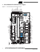
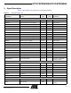
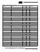
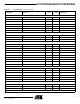
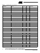
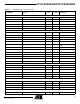
ICE and JTAG
NTRST Test Reset Signal Input Low No pull-up resistor
TCK Test Clock Input No pull-up resistor
TDI Test Data In Input No pull-up resistor
TDO Test Data Out Output
TMS Test Mode Select Input No pull-up resistor
JTAGSEL JTAG Selection Input Pull-down resistor
RTCK Return Test Clock Output
Reset/Test
NRST Microcontroller Reset I/O Low Pull-up resistor
TST Test Mode Select Input Pull-down resistor
BMS Boot Mode Select Input Pull-up resistor
Debug Unit - DBGU
DRXD Debug Receive Data Input
DTXD Debug Transmit Data Output
Advanced Interrupt Controller - AIC
IRQ0 - IRQ1 External Interrupt Inputs Input
FIQ Fast Interrupt Input Input
PIO Controller - PIOA - PIOB - PIOC - PIOD
PA0 - PA31 Parallel IO Controller A I/O Pulled-up input at reset
PB0 - PB31 Parallel IO Controller B I/O Pulled-up input at reset
PC0 - PC31 Parallel IO Controller C I/O Pulled-up input at reset
PD0 - PD31 Parallel IO Controller D I/O Pulled-up input at reset
Direct Memory Access Controller - DMA
DMARQ0-DMARQ3 DMA Requests Input
External Bus Interface - EBI
D0 - D31 Data Bus I/O Pulled-up input at reset
A0 - A25 Address Bus Output 0 at reset
NWAIT External Wait Signal Input Low
Static Memory Controller - SMC
NCS0 - NCS5 Chip Select Lines Output Low
NWR0 - NWR3 Write Signal Output Low
NRD Read Signal Output Low
NWE Write Enable Output Low
NBS0 - NBS3 Byte Mask Signal Output Low
Table 3-1. Signal Description List (Continued)
Signal Name Function Type
Active
Level Comments