Features • • • • • • • • • • • • • • • • • • • • • • • • • • • • • • High FSK Sensitivity: -106 dBm at 20 kBaud/-109.5 dBm at 2.4 kBaud (433.92 MHz) High ASK Sensitivity: -112.5 dBm at 10 kBaud/-116.5 dBm at 2.4 kBaud (433.92 MHz) Low Supply Current: 10.
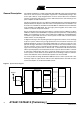
General Description The ATA5811/ATA5812 is a highly integrated UHF ASK/FSK single-channel half-duplex transceiver with low power consumption supplied in a small QFN48 package. The receive part is built as a fully integrated low-IF receiver, whereas direct PLL modulation with the fractional-N synthesizer is used for FSK transmission and switching of the power amplifier for ASK transmission.
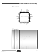
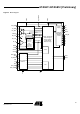
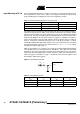
ATA5811/ATA5812 [Preliminary] NC NC RX_ACTIVE T1 T2 T3 T4 T5 PWR_ON RX_TX1 RX_TX2 CDEM Figure 2.
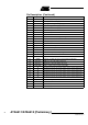
Pin Description (Continued) Pin Symbol 19 VAUX Auxiliary supply voltage input 20 TEST1 Test input, at GND during operation 21 DVCC Blocking of the digital voltage supply 22 VSOUT Output voltage power supply for external devices 23 TEST2 Test input, at GND during operation 24 XTAL1 Reference crystal 25 XTAL2 26 NC 27 VSINT 28 N_RESET Reference crystal Not connected Microcontroller Interface supply voltage Output pin to reset a connected microcontroller 29 IRQ Interrupt request
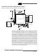
ATA5811/ATA5812 [Preliminary] 433_N868 RF transceiver R_PWR RF_OUT Power Supply TX LNA CDEM Fract.-NFrequency Synthesizer Signal Processing (Mixer, IF Filter, IF Amp., Demodulator, Data Filter Data Slicer) RX/TX FREQ FREF 9 Demod_Out VS2 VS1 VAUX TX_DATA (FSK) PA RX_TX2 RF_IN Frontend Enable Digital Control Logic PA_Enable (ASK) PWR_H RX_TX1 DVCC AVCC RX_ACTIVE Figure 3.
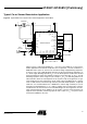
Typical Key Fob or Sensor Application with 1 Battery Figure 4. Typical RKE Key Fob or Sensor Application, 433.
ATA5811/ATA5812 [Preliminary] Typical Car or Sensor Base-station Application Figure 5. Typical RKE Car or Sensor Base-station Application, 433.
Typical Key Fob Application, 2 Batteries Figure 6. Typical RKE Key Fob Application, 433.92 MHz, 2 Batteries C7 NC RX_TX2 T5 T4 T2 T3 RX_TX1 NC PWR_ON NC T1 RX_ACTIVE SCK SDI_TMDI NC C5 433_N868 R1 ATA5811/ATA5812 NC CLK IRQ PWR_H N_RESET VSINT Loop antenna VCC VSS NC TEST2 DVCC VAUX TEST1 VS1 VS2 NC AVCC C9 NC NC C10 NC NC VSOUT RF_OUT C8 Microcontroller SDO_TMDO R_PWR L2 CS DEM_OUT RF_IN AVCC CDEM RSSI XTAL1 NC C6 NC C11 20 mm x 0.4 mm L1 XTAL2 13.
ATA5811/ATA5812 [Preliminary] RF Transceiver According to Figure 3 on page 5, the RF transceiver consists of an LNA (Low-Noise Amplifier), PA (Power Amplifier), RX/TX switch, fractional-N frequency synthesizer and the signal processing part with mixer, IF filter, IF amplifier, FSK/ASK demodulator, data filter and data slicer.
Input Matching at RF_IN The measured input impedances as well as the values of a parallel equivalent circuit of these impedances can be seen in Table 1. The highest sensitivity is achieved with power matching of these impedances to the source impedance of 50 Ω Table 1. Measured Input Impedances of the RF_IN Pin fRF/MHz Z(RF_IN) Rp//Cp 315 (44-j233)Ω 1278 Ω//2.1 pF 433.92 (32-j169)Ω 925 Ω//2.1 pF 868.3 (21-j78)Ω 311 Ω//2.
ATA5811/ATA5812 [Preliminary] Table 3. Measured Sensitivity FSK, ±16 kHz, Manchester, dBm, BER = 10-3 RF Frequency BR_Range_0 1.0 kBaud BR_Range_0 2.4 kBaud BR_Range_1 5.0 kBaud BR_Range_2 10 kBaud BR_Range_3 20 kBaud 315 MHz -110.0 dBm -110.5 dBm -109.0 dBm -108.0 dBm -107.0 dBm 433.92 MHz -109.0 dBm -109.5 dBm -108.0 dBm -107.0 dBm -106.0 dBm 868.3 MHz -106.0 dBm -106.5 dBm -105.5 dBm -104.0 dBm -103.5 dBm Table 4.
As can be seen in Figure 8 on page 11 the supply voltage has almost no influence. The temperature has an influence of about +1.5/-0.7 dB and a frequency offset of ±65 kHz also influences by about ±1 dB. All these influences, combined with the sensitivity of a typical IC, are then within a range of -103.7 dBm and -107.3 dBm over temperature, supply voltage and frequency offset which is -105.5 dBm ±1.8dB.
ATA5811/ATA5812 [Preliminary] Figure 9 shows narrow band blocking and Figure 10 wide band blocking characteristics. The measurements were done with a useful signal of 433.92 MHz/FSK/ 20 kBaud/±16 kHz/Manchester with a level of -106 dBm + 3 dB = -103 dBm which is 3 dB above the sensitivity level. The figures show how much a continuous wave signal can be larger than -103 dBm until the BER is higher than 10-3. The measurements were done at the 50 Ω input according to Figure 7 on page 10.
Table 6 shows the blocking performance measured relative to -100 dBm for some other frequencies. Note that sometimes the blocking is measured relative to the sensitivity level (dBS) instead of the carrier (dBC). Table 6. Blocking 6 dB Above Sensitivity Level with BER < 10-3 Frequency Offset Blocker Level Blocking +0.75 MHz -45 dBm 55 dBC/61 dBS -0.75 MHz -45 dBm 55 dBC/61 dBS +1.5 MHz -38 dBm 62 dBC/68 dBS -1.
ATA5811/ATA5812 [Preliminary] The data filter of the ATA5811/ATA5812 implies a quasi peak detector. This results in a good suppression of the above mentioned disturbers and exhibits a good carrier to Gaussian noise performance. The required useful signal to disturbing signal ratio to be received with a BER of 10 -3 is less than 12 dB in ASK mode and less than 3 dB (BR_Range_0 ... BR_Range_2)/6 dB (BR_Range_3) in FSK mode.
The initial tolerances of the crystal oscillator due to crystal tolerances, internal capacitor tolerances and the parasitics of the board have to be compensated at manufacturing setup with control registers 2 and 3 as can be seen in Table 12 on page 24. The other control words for the synthesizer needed for ASK, FSK and receive/transmit switching are calculated internally. The RF (Radio Frequency) resolution is equal to the XTO frequency divided by 16384 which is 777.1 Hz at 315.0 MHz, 808.9 Hz at 433.
ATA5811/ATA5812 [Preliminary] Figure 14. Unmodulated TX Spectrum fFSK_L Ref 10 dBm Atten 20 dB Samp Log 10 dB/ VAvg 50 W1 S2 S3 FC Center 433.92 MHz Res BW 10 kHz VBW 10 kHz Span 1 MHz Sweep 27.5 ms (401 pts) Figure 15. FSK-modulated TX Spectrum (20 kBaud/±16.17 kHz/Manchester Code) Ref 10 dBm Samp Log 10 dB/ Atten 20 dB VAvg 50 W1 S2 S3 FC Center 433.92 MHz Res BW 10 kHz VBW 10 kHz Span 1 MHz Sweep 27.
Output Power Setting and PA Matching at RF_OUT The Power Amplifier (PA) is a single-ended open collector stage which delivers a current pulse which is nearly independent of supply voltage, temperature and tolerances due to bandgap stabilization. Resistor R1, see Figure 16 on page 19, sets a reference current which controls the current in the PA. A higher resistor value results in a lower reference current, a lower output power and a lower current consumption of the PA.
ATA5811/ATA5812 [Preliminary] Figure 16. Power Setting and Output Matching AVCC C2 L1 C1 ATA5811/ATA5812 10 RF_OUT RFOUT 8 C3 R_PWR R1 VPWR_H 9 PWR_H Table 7. Measured Output Power and Current Consumption with VS1 = VS2 = 3 V, Tamb = 25°C Frequency (MHz) TX Current (mA) Output Power (dBm) R1 (kΩ) 56 RLopt (Ω) L1 (nH) QL1 C1 (pF) C3 (pF) GND 2500 82 28 1.5 0 315 8.5 315 10.5 5.7 27 GND 920 68 32 2.2 0 315 16.7 10.5 27 AVCC 350 56 35 3.9 0 433.92 8.6 0.
Table 8. Measured Output Power and Supply Current at 433.92 MHz, PWR_H = GND VS = 2.4 V 3.0 V 3.6 V Tamb = -40°C 10.19 mA 3.8 dBm 10.19 mA 5.5 dBm 10.78 mA 6.2 dBm Tamb = +25°C 10.62 mA 4.6 dBm 11.19 mA 6.2 dBm 11.79 mA 7.1 dBm Tamb = +105°C 11.4 mA 3.8 dBm 12.02 mA 5.4 dBm 12.73 mA 6.3 dBm Table 9 shows the relative changes of the output power of a typical device compared to 3.0 V/25°C.
ATA5811/ATA5812 [Preliminary] Figure 17. Equivalent Circuit of the Switch RX_TX1 1.6 nH 2.5 pF 11 Ω TX 5Ω Matching Network in TX Mode In TX mode the 20 mm long and 0.4 mm wide transmission line which is much shorter than λ/4 is approximately switched in parallel to the capacitor C9 to GND. The antenna connection between C8 and C9 has an impedance of about 50 Ω locking from the transmission line into the loop antenna with pin RF_OUT, L2, C10 , C8 and C9 connected (using a C9 without the added 7.
Table 11. Impedance RF_OUT Pin in RX Mode Frequency Z(RF_OUT)RX RP//CP 315 MHz 36 Ω − j 502 Ω 7 kΩ / / 1.0 pF 433.92 MHz 19 Ω − j 366 Ω 7 kΩ / / 1.0 pF 868.3 MHz 2.8 Ω − j 141Ω 7 kΩ / / 1.3 pF Note that if matching to 50 Ω, like in Figure 5 on page 7, a high Q wire wound inductor with a Q > 70 should be used for L2 to minimize its contribution to RX losses which will otherwise be dominant. The RX and TX losses will be in the range of 1.0 dB there.
ATA5811/ATA5812 [Preliminary] With Cm ≤14 fF, C0 ≥ 1.5 pF, CLN = 9 pF and CL = 7.6 pF to 10.6 pF the pulling amounts to P ≤±100 ppm and with Cm ≤7 fF, C0 ≥ 1.5 pF, CLN = 9 pF and CL = 7.4 pF to 10.6 pF the pulling is P ≤±50 ppm. Since typical crystals have less than ±50 ppm tolerance at 25° the compensation is not critical. C0 of the XTAL has to be lower than CLmin/2 = 3.
Figure 19. XTO Block Diagram XTAL1 XTAL2 CLK & fXTO 8 pF 10 pF CL1 C L2 S1 10 pF DVCC_OK (from power supply) Divider /3 CLK_ON (Control Register 3) 8 pF Amplitude Detector S2 In IDLE mode and during Sleep mode (RX_Polling) the switches S1 and S2 are open.
ATA5811/ATA5812 [Preliminary] The variable FREQ depends on FREQ2 and FREQ3, which are defined by the bits FR0 to FR8 in control register 2 and 3 and is calculated as follows: FREQ = 3584 + FREQ2 + FREQ3 Only the range of FREQ = 3803 to 4053 of this register should be used because otherwise harmonics of f XTO and f CLK can cause interference with the received signals (FREQ_min = 3803, FREQ_max = 4053). The resulting tuning range is ±118 ppm at 868.3 MHz and more than ±150 ppm at 433.92 MHz or 315 MHz.
Power Supply Figure 21. Power Supply VS1 SW_AVCC V_REG1 IN VS2 OUT AVCC 3.25 V typ. VSINT EN (Control Register 1) ≥1 AVCC_EN PWR_ON T1 FF1 S T5 Q R DVCC_OK OFFCMD ≥1 (Command via SPI) VS1+ 0.55V typ. SW_VSOUT S 0 0 1 1 R 0 1 0 1 Q no change 0 1 1 P_On_Aux DVCC SW_DVCC and V_Monitor (1.5 V typ.) (Status Register) V_Monitor (2.3 V/ 2.38 V typ.) VAUX IN VSOUT_EN V_REG2 OUT 3.25 V typ.
ATA5811/ATA5812 [Preliminary] AVCC is the internal operation voltage of the RF transceiver and is feed via the switch SW_AVCC by VS1. AVCC must be blocked with a 68 nF capacitor (see Figure 4 on page 6, Figure 5 on page 7 and Figure 6 on page 8). DVCC is the internal operation voltage of the digital control logic and is feed via the switch SW_DVCC by VS1 or VSOUT. DVCC must be blocked on pin DVCC with 68 nF (see Figure 4 on page 6, Figure 5 on page 7 and Figure 6 on page 8).
Figure 22. Flow Chart Operation Modes Bit AVCC_EN = 0 and OFF Command and Pin PWR_ON = 0 and Pin T1, T2, T3, T4 and T5 = 1 OFF Mode VVAUX < 3.5 V (typ) AVCC = OFF DVCC = OFF VSOUT = OFF VVAUX > 3.5 V (typ) Pin PWR_ON = 1 or Pin T1, T2, T3, T4 or T5 = 0 VVAUX < VS1+0.5 V AVCC = VS1 DVCC = VS1 VSOUT = VS1 VVAUX > VS1+0.
ATA5811/ATA5812 [Preliminary] AUX Mode The transceiver changes from OFF mode to AUX mode if the voltage at pin VAUX VVAUX > 3.5 V (typically). In AUX mode DVCC and VSOUT are connected to the auxiliary power supply input (VAUX) via the voltage regulator V_REG2. In AUX mode the transceiver is programmable via the 4-wire serial interface, but no RX or TX operations are possible because AVCC = OFF.
If VVSOUT drops below VThres_1 (typically 2.3 V), N_RESET is set to low. If bit VSOUT_EN in control register 3 is 1, a DVCC_RESET is also generated. If VVSOUT was prior disabled by the connected micr ocontroller by setting bit VSOUT_EN = 0, no DVCC_RESET is generated. Note: If VSOUT < VThres_1 (typically 2.3 V) the output of the pin CLK is low, the Microcontroller_Interface is disabled and the transceiver is not programmable via the 4-wire serial interface. Figure 23. Reset Timing VThres_2 = 2.
ATA5811/ATA5812 [Preliminary] Figure 24. Reset Logic, SR Latch Generates the Hysteresis in the NRESET Signal DVCC_OK and ≥1 DVCC_RESET XTO_OK VSOUT_EN and NRESET and S Q R Q VSOUT_OK LOW_BATT 1-Battery Application S R 0 0 0 1 1 0 1 1 Q no change 0 1 no change The supply voltage range is 2.4 V to 3.6 V and VAUX is not used. Figure 25. 1-Battery Application ATA5811/ATA5812 VS1 Microcontroller 2.4 V to 3.
2-Battery Application The supply voltage range is 4.4 V to 6.6 V and VAUX is connected to an inductive supply. Figure 26. 2-Battery Application with Inductive Emergency Supply ATA5811/ATA5812 Microcontroller VS1 VS2 4.4 V to 6.
ATA5811/ATA5812 [Preliminary] After the transceiver is turned on via pin PWR_ON = High, T1 = Low, T2 = Low, T3 = Low, T4 = Low or T5 = Low or the voltage at pin VAUX VVAUX > 3.5 V (typically) the control registers are in the default state. Figure 27.
TX/RX Data Buffer The TX/RX data buffer is used to handle the data transfer during RX and TX operations. Control Register To use the transceiver in different applications it can be configured by a connected microcontroller via the 4-wire serial interface. Control Register 1 (ADR 0) Table 14.
ATA5811/ATA5812 [Preliminary] Table 18. Control Register 1 (Function of Bit 2 and Bit 1) OPM1 OPM0 Function 0 0 Idle mode (default) 0 1 TX mode 1 0 RX polling mode 1 1 RX mode Table 19. Control Register 1 (Function of Bit 0) T_MODE Function 0 TX and RX function via TX/RX data buffer (default) 1 Transparent mode, TX/RX data buffer disabled, TX modulation data stream via pin SDI_TMDI, RX modulation data stream via pin SDO_TMDO Control Register 2 (ADR 1) Table 20.
Control Register 3 (ADR 2) Table 23. Control Register 3 (Function of Bit 3 and Bit 2) FR8 FR7 Function 0 0 FREQ3 = 0 0 1 FREQ3 = 128 1 0 FREQ3 = 256 (default) 1 1 FREQ3 = 384 Tuning of fRF MSB’s Note: Table 24.
ATA5811/ATA5812 [Preliminary] Table 28. Control Register 4 (Function of Bit 1) XSleep Function 0 XSleep = 1; extended TSleep off (default) 1 XSleep = 8; extended TSleep on Table 29. Control Register 4 (Function of Bit 0) XLim Function 0 XLim = 1; extended TLim_min, TLim_max off (default) 1 XLim = 2; extended TLim_min, TLim_max on Control Register 5 (ADR 4) Table 30.
Table 32. Control Register 5 (Function of Bit 5, Bit 4, Bit 3, Bit 2, Bit 1 and Bit 0 in TX Mode) Lim_min5 Lim_min4 Lim_min3 Lim_min2 Lim_min1 Lim_min0 Function (TX Mode) Lim_min (Lim_min < 10 are not applicable) (TX_Baudrate = 1/((Lim_min + 1) × TXDCLK × 2) 0 0 1 0 1 0 10 0 0 1 0 1 1 11 . . . . . . 0 1 0 0 0 0 . . . . . . 1 1 1 1 1 1 16 (TX_Baudrate = 1/((16 + 1) × TXDCLK × 2) (default) 63 Control Register 6 (ADR 5) Table 33.
ATA5811/ATA5812 [Preliminary] Status Register The status register indicates the current status of the transceiver and is readable via the 4-wire serial interface. Setting Power_On or P_On_Aux or an event on ST1, ST2, ST3, ST4 or ST5 is indicated by an IRQ. Reading the status register resets the bits Power_On, Low_Batt, P_On_Aux and the IRQ Status Register (ADR 8) Table 35.
Pin Tn To switch the transceiver from OFF to Idle mode, pin Tn must set to 0 (maximum 0.2 × VVS2) for at least TTn_IRQ (see Figure 28). The transceiver recognize the negative edge, sets pin N_RESET to low and switches on DVCC, AVCC and the power supply for external devices VSOUT. If VDVCC exceeds 1.5 V (typically) and the XTO is settled, the digital control logic is active and sets the status bit STn to 1 and an interrupt is issued (TTn_IRQ). After the voltage on pin VSOUT exceeds 2.
ATA5811/ATA5812 [Preliminary] If the transceiver is in any active mode (Idle, AUX, TX, RX, RX_Polling), an integrated debounce logic is active. If there is an event on pin Tn a debounce counter is set to 0 (T = 0) and started. The status is updated, an interrupt is issued and the debounce counter is stopped after reaching the counter value T = 8195 × TDCLK. An event on the same key input before reaching T = 8195 × TDCLK stops the debounce counter.
Pin PWR_ON To switch the transceiver from OFF to Idle mode, pin PWR_ON must set to 1 (minimum 0.8 × VVS2) for at least TPWR_ON (see Figure 30). The transceiver recognize the positive edge, sets pin N_RESET to low and switches on DVCC, AVCC and the power supply for external devices VSOUT. If VDVCC exceeds 1.5 V (typically) and the XTO is settled, the digital control logic is active and sets the status bit Power_On to 1 and an interrupt is issued (TPWR_ON_IRQ_1). After the voltage on pin VSOUT exceeds 2.
ATA5811/ATA5812 [Preliminary] Low Battery Indicator The status bit Low_Batt is set to 1 if the voltage on pin VSOUT V VSOUT drops under 2.38 V (typically). Low_Batt is set to 0 if VVSOUT exceeds VThres_2 and the status register is read via the 4-wire serial interface (see Figure 23 on page 30). Figure 31. Timing Status Bit Low_Batt IDLE, AUX, TX, RX or RX Polling Mode V VSOUT < 2.
Pin VAUX To switch the transceiver from OFF to AUX mode, the voltage on pin VAUX VVAUX must exceed 3.5 V (typically) (see Figure 32). If VVAUX exceeds 2 V (typically) pin N_RESET is set to low, DVCC and the power supply for external devices VSOUT are switched on. If VVAUX exceeds 3.5 V (typically) the status bit P_On_Aux is set to 1 and an interrupt is issued. After the voltage on pin VSOUT exceeds 2.3 V (typically) and the start-up time of the XTO is elapsed the output clock on pin CLK is available.
ATA5811/ATA5812 [Preliminary] Transceiver Configuration The configuration of the transceiver takes place via a 4-wire serial interface (CS, SCK, SDI_TMDI, SDO_TMDO) and is organized in 8-bit units. The configuration is initiated with a 8-bit command. While shifting the command into pin SDI_TMDI, the number of bytes in the TX/RX data buffer are available on pin SDO_TMDO. The read and write commands are followed by one or more 8-bit data units. Each 8-bit data transmission begins with the MSB.
Command: Write Control Register The control registers can be written individually or successively. An echo of the command and the data bytes are provided for the microcontroller on pin SDO_TMDO. Figure 36. Write Control Register MSB LSB MSB LSB MSB LSB SDI_TMDI Command: Write Control Register X Data Control Register X Command: Write Control Register Y SDO_TMDO Nr.
ATA5811/ATA5812 [Preliminary] . Table 36.
Operation Modes RX Operation The transceiver is set to RX operation with the bits OPM0 and OPM1 in control register 1 . Table 37. Control Register 1 OPM1 OPM0 Function 1 0 RX polling mode 1 1 RX mode The transceiver is designed to consume less than 1 mA in RX operation while being sensitive to signals from a corresponding transmitter. This is achieved via the polling circuit. This circuits enables the signal path periodically for a short time.
ATA5811/ATA5812 [Preliminary] To save current it is recommended CLK and V VSOUT be disabled during RX polling mode. IP does not include the current of the Microcontroller_Interface IVSINT and the current of an external device connected to pin VSOUT (e.g., microcontroller).
Figure 40. Flow Chart Polling Mode/RX Mode (T_MODE = 1, Transparent Mode Inactive) Start RX Polling Mode Sleep mode: All circuits for analog signal processing are disabled. Only XTO and Polling logic is enabled. Output level on pin RX_ACTIVE -> Low; IS = IIDLE_X TSleep = Sleep × 1024 × TDCLK × XSleep Sleep: XSleep: TDCLK: Defined by bits Sleep0 to Sleep4 in Control Register 4 Defined by bit XSleep in Control Register 4 Basic clock cycle TStartup_PLL: 798.
ATA5811/ATA5812 [Preliminary] Figure 41. Flow Chart Polling Mode/RX Mode (T_MODE = 1, Transparent Mode Active) Start RX Polling Mode Sleep mode: All circuits for analog signal processing are disabled. Only XTO and Polling logic is enabled. Output level on pin RX_ACTIVE -> Low; IS = IIDLE_X TSleep = Sleep × 1024 × TDCLK × XSleep Sleep: XSleep: TDCLK: Defined by bits Sleep0 to Sleep4 in Control Register 4 Defined by bit XSleep in Control Register 4 Basic clock cycle TStartup_PLL: 798.
Bit-check Mode In Bit-check mode the incoming data stream is examined to distinguish between a valid signal from a corresponding transmitter and signals due to noise. This is done by subsequent time frame checks where the distance between 2 signal edges are continuously compared to a programmable time window. The maximum count of this edge to edge test before the transceiver switches to receiving mode is also programmable.
ATA5811/ATA5812 [Preliminary] For the best noise immunity it is recommended to use a low span between TLim_min and TLim_max. This is achieved using a fixed frequency at a 50% duty cycle for the transmitter preburst. A '11111...' or a '10101...' sequence in Manchester or Bi-phase is a good choice concerning that advice.
Figure 45. Timing Diagram for Failed Bit-check (Condition CV_Lim < Lim_min) (Lim_min = 14, Lim_max = 24) RX_ACTIVE Bit check failed (CV_Lim < Lim_min) Bit check 1/2 Bit Demod_Out Bit-check counter 0 1 2 3 4 5 6 7 8 1 2 3 4 5 6 7 8 9 101112 T Startup_Sig_Proc TBit-check Start-up mode 0 TSleep Bit-check mode Sleep mode Figure 46.
ATA5811/ATA5812 [Preliminary] In the presence of a valid transmitter signal, TBit-check is dependent on the frequency of that signal, fSig, and the count of the bits, NBit-check. A higher value for NBit-check thereby results in a longer period for TBit-check requiring a higher value for the transmitter preburst TPreburst. Receiving Mode If the Bit-check was successful for all bits specified by NBit-check, the transceiver switches to receiving mode.
If the TX/RX data buffer control logic detects the start bit, the data stream is written in the TX/RX data buffer byte by byte. The start bit is part of the first data byte and must be different from the bits of the preburst. If the preburst consists of a sequence of '00000...', the start bit must be a 1. If the preburst consists of a sequence of '11111...', the start bit must be a 0.
ATA5811/ATA5812 [Preliminary] Figure 49. Bit Error (TMODE = 0) Bit check ok Bit error Demod_Out Byte n-1 Byte n Byte n+1 Receiving mode Preburst Start-up mode Bit-check mode Byte 1 Receiving mode Table 38.
TX Operation The transceiver is set to TX operation by using the bits OPM0 and OPM1 in the control register 1. Table 40. Control Register 1 OPM1 OPM0 Function 0 1 TX mode Before activating TX mode, the TX parameters (baud rate, modulation scheme ... ) must be selected as illustrated in Figure 50 on page 59. The baud rate depends on Baud 0 and Baud 1 in control register 6, Lim_min0 to Lim_min5 in control register 5 and XLIM in control register 4 (see section “Control Register”).
ATA5811/ATA5812 [Preliminary] Figure 50. TX Operation (T_MODE = 0) Write Control Register 6 Baud1, Baud0: Lim_max0 ... Lim_max5: Select Baudrate Range Don't care Write Control Register 5 Lim_min0 ... Lim_min5: Bitchk0, Bitchk1: Select the baud rate Don't care Write Control Register 4 XLim: ASK/_NFSK: Sleep0 ...
Figure 51. TX Transparent Mode (T_MODE = 1) Write Control Register 4 XLim: ASK/_NFSK: Sleep0 ... Sleep4: XSleep: Don't care Select modulation Don't care Don't care Write Control Register 3 FR7, FR8: VSOUT_EN: CLK_ON: Adjust fRF Set VSOUT_EN = 1 Don't care Write Control Register 2 FR0 ...
ATA5811/ATA5812 [Preliminary] Table 41.
Absolute Maximum Ratings Stresses beyond those listed under “Absolute Maximum Ratings” may cause permanent damage to the device. This is a stress rating only and functional operation of the device at these or any other conditions beyond those indicated in the operational sections of this specification is not implied. Exposure to absolute maximum rating conditions for extended periods may affect device reliability. Parameters Symbol Max.
ATA5811/ATA5812 [Preliminary] Electrical Characteristics: General All parameters refer to GND and are valid for Tamb = -40°C to +105°C, VVS1 = VVS2 = 2.4 V to 3.6 V (1-battery application), VVS2 = 4.4 V to 6.6 V (2-battery application) and VVS2 = VVAUX = 4.75 V to 5.25 V (car application). Typical values are given at VVS1 = VVS2 = 3 V and Tamb = 25°C, fRF = 433.92 MHz (1-battery application) unless otherwise specified.
Electrical Characteristics: General (Continued) All parameters refer to GND and are valid for Tamb = -40°C to +105°C, VVS1 = VVS2 = 2.4 V to 3.6 V (1-battery application), VVS2 = 4.4 V to 6.6 V (2-battery application) and VVS2 = VVAUX = 4.75 V to 5.25 V (car application). Typical values are given at VVS1 = VVS2 = 3 V and Tamb = 25°C, fRF = 433.92 MHz (1-battery application) unless otherwise specified.
ATA5811/ATA5812 [Preliminary] Electrical Characteristics: General (Continued) All parameters refer to GND and are valid for Tamb = -40°C to +105°C, VVS1 = VVS2 = 2.4 V to 3.6 V (1-battery application), VVS2 = 4.4 V to 6.6 V (2-battery application) and VVS2 = VVAUX = 4.75 V to 5.25 V (car application). Typical values are given at VVS1 = VVS2 = 3 V and Tamb = 25°C, fRF = 433.92 MHz (1-battery application) unless otherwise specified.
Electrical Characteristic: 1-Battery Application (Continued) All parameters refer to GND and are valid for Tamb = -40°C to +105°C, V VS1 = V VS2 = 2.4 V to 3.6 V typical values at VVS1 = VVS2 = 3 V and Tamb = 25°C. Application according to Figure 4 on page 6. fRF = 315.0 MHz/433.92 MHz/868.3 MHz unless otherwise specified No. 9.3 Parameters Power supply output voltage Test Conditions Pin Symbol Min. 1-battery application VVS1 = VVS2 ≥ 2.6 V VAUX open (1) IVSOUT ≤13.
ATA5811/ATA5812 [Preliminary] Electrical Characteristic: 1-Battery Application (Continued) All parameters refer to GND and are valid for Tamb = -40°C to +105°C, V VS1 = V VS2 = 2.4 V to 3.6 V typical values at VVS1 = VVS2 = 3 V and Tamb = 25°C. Application according to Figure 4 on page 6. fRF = 315.0 MHz/433.92 MHz/868.3 MHz unless otherwise specified No. Parameters Test Conditions Pin Symbol 9.
Electrical Characteristics: 2-Battery Application All parameters refer to GND and are valid for Tamb = -40 °C to +105 °C, VVS2 = 4.4 V to 6.6 V typical values at VVS2 = 6V and Tamb = 25°C. Application according to Figure 6 on page 8. f RF = 315.0MHz/433.92 MHz/868.3 MHz unless otherwise specified No. Parameters 10 2-Battery Application Test Conditions Pin Symbol Min. IIDLE_VS2 or IRX_VS2 or IStartup_PLL_VS2 or ITX_VS2 Typ. Max.
ATA5811/ATA5812 [Preliminary] Electrical Characteristics: 2-Battery Application (Continued) All parameters refer to GND and are valid for Tamb = -40 °C to +105 °C, VVS2 = 4.4 V to 6.6 V typical values at VVS2 = 6V and Tamb = 25°C. Application according to Figure 6 on page 8. f RF = 315.0MHz/433.92 MHz/868.3 MHz unless otherwise specified No. Parameters Test Conditions 10.11 Supply current RX mode CLK enabled VVSOUT enabled 10.12 Current during TStartup_PLL on pin VS2 IVSOUT = 0 10.
Electrical Characteristics: Car Application All parameters refer to GND and are valid for Tamb = -40°C to +105°C, VVS2 = 4.75 V to 5.25 V. Typical values at VVS2 = 5 V and Tamb = 25°C. Application according to Figure 5 on page 7. fRF = 315.0 MHz/433.92 MHz/868.3 MHz unless otherwise specified No. Parameters Test Conditions Pin Symbol Min. Typ. Max.
ATA5811/ATA5812 [Preliminary] Electrical Characteristics: Car Application (Continued) All parameters refer to GND and are valid for Tamb = -40°C to +105°C, VVS2 = 4.75 V to 5.25 V. Typical values at VVS2 = 5 V and Tamb = 25°C. Application according to Figure 5 on page 7. fRF = 315.0 MHz/433.92 MHz/868.3 MHz unless otherwise specified No. 11.11 Parameters Test Conditions Current during TStartup_PLL on pin VS2 and VAUX IVSOUT = 0 Pin Symbol 17, 19 IStartup_PLL_VS2_ Min. Typ. Max. Unit Type* 9.
Digital Timing Characteristics All parameters refer to GND and are valid for Tamb = -40°C to +105°C. VVS1 = VS2 = 2.4 V to 3.6 V (1-battery application), V V S2 = 4.4 V to 6.6 V (2-batter y application) and V V S2 = 4.75 V to 5.25 V (car application), typical values at VVS1 = VVS2 = 3 V and Tamb = 25°C unless otherwise specified. No. Parameters 12 Basic Clock Cycle of the Digital Circuitry 12.1 Test Conditions Basic clock cycle Pin Symbol Min. TDCLK Typ. Max.
ATA5811/ATA5812 [Preliminary] Digital Timing Characteristics (Continued) All parameters refer to GND and are valid for Tamb = -40°C to +105°C. VVS1 = VS2 = 2.4 V to 3.6 V (1-battery application), V V S2 = 4.4 V to 6.6 V (2-batter y application) and V V S2 = 4.75 V to 5.25 V (car application), typical values at VVS1 = VVS2 = 3 V and Tamb = 25°C unless otherwise specified. No. 13.5 Parameters Test Conditions Baud-rate range BR_Range = BR_Range0 BR_Range1 BR_Range2 BR_Range3 Pin Symbol BR_Range Min.
Digital Timing Characteristics (Continued) All parameters refer to GND and are valid for Tamb = -40°C to +105°C. VVS1 = VS2 = 2.4 V to 3.6 V (1-battery application), V V S2 = 4.4 V to 6.6 V (2-batter y application) and V V S2 = 4.75 V to 5.25 V (car application), typical values at VVS1 = VVS2 = 3 V and Tamb = 25°C unless otherwise specified. No. Parameters 15.9 Pin Symbol Min. Time period SCK low to CS high 33, 35 TSCK_setup1 15.10 Time period SCK low to CS low 33, 35 15.
ATA5811/ATA5812 [Preliminary] Digital Timing Characteristics (Continued) All parameters refer to GND and are valid for Tamb = -40°C to +105°C. VVS1 = VS2 = 2.4 V to 3.6 V (1-battery application), V V S2 = 4.4 V to 6.6 V (2-batter y application) and V V S2 = 4.75 V to 5.25 V (car application), typical values at VVS1 = VVS2 = 3 V and Tamb = 25°C unless otherwise specified. No. Parameters Test Conditions 16.
Digital Port Characteristics All parameter refer to GND and valid for Tamb = -40 °C to +105 °C, VVS1 = VS2 = 2.4 V to 3.6 V (1 Battery Application) and V VS 2 = 4.4 V to 6.6 V (2 Batter y Application) and V V S2 = 4.75 V to 5.25 V (Car Application) typical values at VVS1 = VVS2 = 3V and Tamb = 25°C unless otherwise specified No. Parameters 17 Digital Ports 17.1 17.2 17.3 Test Conditions Pin Symbol CS input V = 2.4 V to 5.
ATA5811/ATA5812 [Preliminary] Digital Port Characteristics (Continued) All parameter refer to GND and valid for Tamb = -40 °C to +105 °C, VVS1 = VS2 = 2.4 V to 3.6 V (1 Battery Application) and V VS 2 = 4.4 V to 6.6 V (2 Batter y Application) and V V S2 = 4.75 V to 5.25 V (Car Application) typical values at VVS1 = VVS2 = 3V and Tamb = 25°C unless otherwise specified No. 17.9 17.10 Parameters Pin Symbol Max. Unit Type* PWR_H input -Low level input voltage 9 VIl 0.
Ordering Information Extended Type Number Package Remarks ATA5811-PLQC QFN48 7 mm × 7 mm ATA5812-PLQC QFN48 7 mm × 7 mm Package Information 88 ATA5811/ATA5812 [Preliminary] 4689B–RKE–04/04
ATA5811/ATA5812 [Preliminary] Table of Contents Features ................................................................................................. 1 Applications .......................................................................................... 1 Benefits .................................................................................................. 1 General Description .............................................................................. 2 Pin Description .....................
Atmel Corporation 2325 Orchard Parkway San Jose, CA 95131, USA Tel: 1(408) 441-0311 Fax: 1(408) 487-2600 Regional Headquarters Europe Atmel Sarl Route des Arsenaux 41 Case Postale 80 CH-1705 Fribourg Switzerland Tel: (41) 26-426-5555 Fax: (41) 26-426-5500 Asia Room 1219 Chinachem Golden Plaza 77 Mody Road Tsimshatsui East Kowloon Hong Kong Tel: (852) 2721-9778 Fax: (852) 2722-1369 Japan 9F, Tonetsu Shinkawa Bldg.