Features • • • • • • • • Single Package Fully-integrated ROM Mask 4-bit Microcontroller with RF Transmitter Low Power Consumption in Sleep Mode (< 1 µA Typically) Maximum Output Power (10 dBm) with Low Supply Current (9.5 mA Typically) 2.0 V to 4.0 V Operation Voltage for Single Li-cell Power Supply -40°C to +125°C Operation Temperature SSO24 Package About Seven External Components Flash Controller for Application Program Available Description The ATAR862-4 is a single package triple-chip circuit.
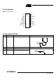
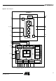
Pin Configuration Figure 2. Pinning SSO24 XTAL VS GND ENABLE NRESET BP63/T3I BP20/NTE BP23 BP41/T2I/VMI BP42/T2O BP43/SD/INT3 VSS 1 2 3 4 5 6 7 8 9 10 11 12 24 23 22 21 20 19 18 17 16 15 14 13 ANT1 ANT2 PA_ENABLE CLK BP60/T3O OSC2 OSC1 BP50/INT6 BP52/INT1 BP53/INT1 BP40/SC/INT3 VDD Pin Description: RF Part Pin Symbol 1 XTAL Function Configuration Connection for crystal VS 1.5k VS 1.
ATAR862-4 Pin Description: RF Part (Continued) Pin Symbol 21 CLK Function Configuration Clock output signal for microcontroller The clock output frequency is set by the crystal to fXTAL/4 VS 100 CLK 100 22 PA_ENABLE Switches on power amplifier, used for ASK modulation PA_ENABLE 50k Uref=1.1V 20 mA 23 ANT2 Emitter of antenna output stage 24 ANT1 Open collector antenna output ANT1 ANT2 Pin Description: Microcontroller Part Pin-No.
UHF ASK/FSK Transmitter Block Features • • • • • • • • • Integrated PLL Loop Filter ESD Protection (4 kV HBM/200 V MM, Except Pin 2: 4 kV HBM/100 V MM) also at ANT1/ANT2 Maximum Output Power (10 dBm) with Low Supply Current (9.
ATAR862-4 Figure 3. Block Diagram ATAR862-4 ENABLE Power up / down CLK f 4 f 32 PFD VS PA_ENABLE GND CP ANT2 LF XTAL ANT1 PA VCO XTO PLL OSC2 OSC1 V DD V SS µC Brown-out protect.
General Description The fully-integrated PLL transmitter that allows particularly simple, low-cost RF miniature transmitters to be assembled. The VCO is locked to 32 fXTAL, thus, a 13.56 MHz crystal is needed for a 433.92 MHz transmitter. All other PLL and VCO peripheral elements are integrated. The XTO is a series resonance oscillator so that only one capacitor together with a crystal connected in series to GND are needed as external elements.
ATAR862-4 Figure 4. Tolerances of Frequency Modulation ~ VS CStray2 CStray1 XTAL ~ CM LM RS C0 Crystal equivalent circuit C4 C5 CSwitch Using C4 = 9.2 pF ±2%, C5 = 6.8 pF ±5%, a switch port with CSwitch = 3 pF ±10%, stray capacitances on each side of the crystal of C Stray1 = C Stray2 = 1 pF ±10%, a parallel capacitance of the crystal of C0 = 3.2 pF ±10% and a crystal with CM = 13 fF ±10%, an FSK deviation of ±21 kHz typical with worst case tolerances of ±16.3 kHz to ±28.8 kHz results.
Figure 5. Output Power Measurement VS C1 = 1n L1 = 33n ~ Power meter Z = 50 W ANT1 ZLopt C2 = 2.2p Rin 50 W ANT2 ~ Application Circuit For the supply-voltage blocking capacitor C3, a value of 68 nF/X7R is recommended (see Figure 6 and Figure 7). C1 and C2 are used to match the loop antenna to the power amplifier where C1 typically is 8.
ATAR862-4 Figure 6.
Figure 7.
ATAR862-4 Figure 8. ESD Protection Circuit VS ANT1 CLK PA_ENABLE ANT2 XTAL ENABLE GND Absolute Maximum Ratings Parameters Symbol Min. Max. Unit Supply voltage VS 5 V Power dissipation Ptot 100 mW Junction temperature Tj 150 °C Storage temperature Tstg -55 125 °C Ambient temperature Tamb -55 125 °C Thermal Resistance Parameters Junction ambient Symbol Value Unit RthJA 170 K/W Electrical Characteristics VS = 2.0 V to 4.
Electrical Characteristics (Continued) VS = 2.0 V to 4.0 V, Tamb = -40°C to 125°C unless otherwise specified. Typical values are given at VS = 3.0 V and Tamb = 25°C. All parameters are referred to GND (Pin 7). Parameters Test Conditions Output power variation for the full temperature range Tamb = -40°C to +85°C VS = 3.0 V VS = 2.0 V Output power variation for the full temperature range Tamb = -40°C to +125°C VS = 3.0 V VS = 2.
ATAR862-4 Microcontroller Block Features • • • • • • • • • • • • • Description Extended Temperature Range for High Temperature up to 125°C 4-Kbyte ROM, 256 x 4-bit RAM 16 Bi-directional I/Os Up to Seven External/Internal Interrupt Sources Multifunction Timer/Counter – IR Remote Control Carrier Generator – Biphase-, Manchester- and Pulse-width Modulator and Demodulator – Phase Control Function Programmable System Clock with Prescaler and Five Different Clock Sources Supply-voltage Range (2.0 V to 4.
Introduction The ATAR862-4 is a member of Atmel’s family of 4-bit single-chip microcontrollers. It contains ROM, RAM, parallel I/O ports, two 8-bit programmable multifunction timer/counters, voltage supervisor, interval timer with watchdog function and a sophisticated on-chip clock generation with integrated RC-, 32-kHz and 4-MHz crystal oscillators. Table 1.
ATAR862-4 ROM The program memory (ROM) is mask programmed with the customer application program during the fabrication of the microcontroller. The ROM is addressed by a 12-bit wide program counter, thus predefining a maximum program bank size of 4 Kbytes.
Figure 12. RAM Map RAM (256 x 4-bit) Autosleep RAM address register: FCh Expression stack 3 0 TOS TOS-1 TOS-2 FFh Global variables X SP 4-bit Y SP Expression stack TOS-1 Return stack 11 0 RP Return stack RP 04h Global v variables 07h 03h 00h 12-bit Registers The microcontroller has seven programmable registers and one condition code register (see Figure 13).
ATAR862-4 RAM Address Registers The RAM is addressed with the four 8-bit wide RAM address registers: SP, RP, X and Y. These registers allow access to any of the 256 RAM nibbles. Expression Stack Pointer (SP) The stack pointer contains the address of the next-to-top 4-bit item (TOS-1) of the expression stack. The pointer is automatically pre-incremented if a nibble is moved onto the stack or post-decremented if a nibble is removed from the stack.
ALU The 4-bit ALU performs all the arithmetic, logical, shift and rotate operations with the top two elements of the expression stack (TOS and TOS-1) and returns the result to the TOS. The ALU operations affects the carry/borrow and branch flag in the condition code register (CCR). Figure 14. ALU Zero-address Operations RAM SP TOS-1 TOS TOS-2 TOS-3 TOS-4 ALU CCR I/O Bus The I/O ports and the registers of the peripheral modules are I/O mapped.
ATAR862-4 Interrupt Processing For processing the eight interrupt levels, the MARC4 includes an interrupt controller with two 8-bit wide interrupt pending and interrupt active registers. The interrupt controller samples all interrupt requests during every non-I/O instruction cycle and latches these in the interrupt pending register. If no higher priority interrupt is present in the interrupt active register, it signals the CPU to interrupt the current program execution.
Table 2.
ATAR862-4 Master Reset The master reset forces the CPU into a well-defined condition. It is unmaskable and is activated independent of the current program state. It can be triggered by either initial supply power-up, a short collapse of the power supply, brown-out detection circuitry, watchdog time-out, or an external input clock supervisor stage (see Figure 9). A master reset activation will reset the interrupt enable flag, the interrupt pending register and the interrupt active register.
A power-on reset pulse is generated by a VDD rise across the default BOT voltage level (1.7 V). A brown-out reset pulse is generated when VDD falls below the brown-out voltage threshold. Two values for the brown-out voltage threshold are programmable via the BOT-bit in the SC-register. When the controller runs in the upper supply voltage range with a high system clock frequency, the high threshold must be used.
ATAR862-4 Figure 18.
Figure 19. Internal Supply Voltage Supervisor VMS = 1 V Low threshold Middle threshold High threshold DD 3.0 V 2.6 V 2.2 V Low threshold Middle threshold High threshold VMS = 0 Figure 20. External Input Voltage Supervisor Internal reference level VMI Negative slope Interrupt positive slope VMS = 1 VMS = 1 VMS = 0 VMS = 0 1.
ATAR862-4 Figure 21. Clock Module RC oscillator 1 Ext. clock OSC1 Oscin SYSCL ExOut Stop ExIn * RC oscillator2 Stop RCOut2 Stop R Trim RCOut1 Control IN1 Cin /2 /2 4-MHz oscillator Oscin Oscout /2 /2 IN2 Divider 4Out Stop 32-kHz oscillator OSC2 Oscout * Oscin Oscout 32Out Osc-Stop CM: Sleep WDL Cin/16 NSTOP CCS CSS1 SUBCL CSS0 32 kHz * mask option SC: BOT --- OS1 OS0 Table 4.
Figure 22. RC-oscillator 1 RC oscillator 1 RcOut1 RcOut1 Osc-Stop Stop Control External Input Clock The OSC1 or OSC2 (mask option) can be driven by an external clock source provided it meets the specified duty cycle, rise and fall times and input levels. Additionally, the external clock stage contains a supervisory circuit for the input clock. The supervisor function is controlled via the OS1, OS0-bit in the SC-register and the CCS-bit in the CMregister.
ATAR862-4 Figure 24. RC-oscillator 2 V DD RC oscillator 2 R ext RcOut2 RcOut2 OSC1 R Trim Osc-Stop Stop OSC2 4-MHz Oscillator The microcontroller block 4-MHz oscillator options need a crystal or ceramic resonator connected to the OSC1 and OSC2 pins to establish oscillation. All the necessary oscillator circuitry is integrated, except the actual crystal, resonator, C3 and C4.
Figure 26. 32-kHz Crystal Oscillator OSC1 Oscin XTAL 32 kHz C1 32Out 32Out * 32-kHz oscillator Oscout OSC2 * * C2 mask option Clock Management The clock management register controls the system clock divider and synchronization stage. Writing to this register triggers the synchronization cycle.
ATAR862-4 System Configuration Register (SC) Primary register address: "3"hex SC: write Bit 2 Bit 1 Bit 0 BOT – OS1 OS0 BOT Brown-Out Threshold BOT = 1, low brown-out voltage threshold (1.7 V) BOT = 0, high brown-out voltage threshold (2.
The microcontroller block has various power-down modes. During the sleep mode the clock for the MARC4 core is stopped. With the NSTOP-bit in the clock management register (CM), it is programmable if the clock for the on-chip peripherals is active or stopped during the sleep mode. If the clock for the core and the peripherals is stopped, the selected oscillator is switched off. An exception is the 32-kHz oscillator, if it is selected it runs continuously independent of the NSTOP-bit.
ATAR862-4 Figure 27. Example of I/O Addressing Module M1 Module ASW Module M2 (Address Pointer) Bank of Subaddress Reg. Primary Reg. Auxiliary Switch Module Aux. Reg. Subport Fh 1 Module M3 5 Subport Eh Subport 1 Primary Reg. Primary Reg. Primary Reg. Subport 0 2 3 6 4 I/O bus to other modules Indirect Subport Access Dual Register Access (Subport Register Write) (Primary Register Write) 1 Addr. (SPort) Addr. (M1) OUT 2 SPort _Data Addr. (M1) OUT 1 Addr. (SPort) Addr.
Table 6.
ATAR862-4 Bi-directional Ports With the exception of Port 1 and Port 6, all other ports (2, 4 and 5) are 4 bits wide. Port 1 and Port 6 have a data width of 2 bits (bit 0 and bit 3). All ports may be used for data input or output. All ports are equipped with Schmitt trigger inputs and a variety of mask options for open-drain, open-source, full-complementary outputs, pull-up and pull-down transistors.
Figure 28. Bi-directional Port 1 V DD I/O Bus * (Data out) D * Q Static pull-up Switched pull-up BP1y P1DATy R * V DD Reset (Direction) * OUT S Q *) Mask options IN R Static pull-down Switched pull-down NQ Master reset Bi-directional Port 2 As all other bi-directional ports, this port includes a bitwise programmable Control Register (P2CR), which enables the individual programming of each port bit as input or output.
ATAR862-4 Port 2 Data Register (P2DAT) Primary register address: "2"hex Bit 3 * Bit 2 Bit 1 Bit 0 P2DAT3 P2DAT2 P2DAT1 P2DAT0 Reset value: 1111b * Bit 3 -> MSB, Bit 0 -> LSB Port 2 Control Register (P2CR) Auxiliary register address: "2"hex Bit 3 Bit 2 Bit 1 Bit 0 P2CR3 P2CR2 P2CR1 P2CR0 Reset value: 1111b Value: 1111b means all pins in input mode Bi-directional Port 5 Code 3210 Function xxx1 BP20 in input mode xxx0 BP20 in output mode xx1x BP21 in input mode xx0x BP21 in outp
Figure 30. Bi-directional Port 5 Switched pull-up I/O Bus V * V DD Static * pull-up DD (Data out) * I/O Bus Q D P5DATy BP5y S V * DD Master reset * * IN enable Static Pull-down Switched pull-down * Mask options Figure 31. Port 5 External Interrupts INT1 INT6 Data in Data in BP52 BP51 Bidir. Port Bidir. Port IN_Enable IN_Enable I/O-bus I/O-bus Data in Data in BP53 BP50 Bidir. Port Bidir.
ATAR862-4 Table 7.
Port 4 Data Register (P4DAT) Primary register address: "4"hex Bit 3 Bit 2 Bit 1 Bit 0 P4DAT3 P4DAT2 P4DAT1 P4DAT0 Port 4 Control Register (P4CR) Byte Write Reset value: 1111b Auxiliary register address: "4"hex First write cycle Second write cycle Bit 3 Bit 2 Bit 1 Bit 0 P41M2 P41M1 P40M2 P40M1 Bit 7 Bit 6 Bit 5 Bit 4 P43M2 P43M1 P42M2 P42M1 Reset value: 1111b Reset value: 1111b P4xM2, P4xM1 – Port 4x Interrupt mode/direction code Auxiliary Address: "4"hex First Write Cycle
ATAR862-4 Port 6 Data Register (P6DAT) Primary register address: "6"hex Bit 3 Bit 2 Bit 1 Bit 0 P6DAT3 – – P6DAT0 Port 6 Control Register (P6CR) Reset value: 1xx1b Auxiliary register address: "6"hex Bit 3 Bit 2 Bit 1 Bit 0 P63M2 P63M1 P60M2 P60M0 Reset value: 1111b P6xM2, P6xM1 – Port 6x Interrupt mode/direction code Auxiliary Address: "6"hex Code 3210 Function Code 3210 Write Cycle Function xx11 BP60 in input mode 11xx BP63 in input mode xx10 BP60 in output mode 10xx BP63 in
Figure 33.
ATAR862-4 This timer starts running automatically after any power-on reset! If the watchdog function is not activated, the timer can be restarted by writing into the T1C1 register with T1RM = 1. Timer 1 can also be used as a watchdog timer to prevent a system from stalling. The watchdog timer is a 3-bit counter that is supplied by a separate output of Timer 1. It generates a system reset when the 3-bit counter overflows. To avoid this, the 3-bit counter must be reset before it overflows.
Timer 1 Control Register 1 (T1C1) Address: "7"hex - Subaddress: "8"hex Bit 3 * Bit 2 Bit 1 Bit 0 T1RM T1C2 T1C1 T1C0 Reset value: 1111b * Bit 3 -> MSB, Bit 0 -> LSB T1RM Timer 1 Restart Mode T1RM = 0, write access without Timer 1 restart T1RM = 1, write access with Timer 1 restart Note: If WDL = 0, Timer 1 restart is impossible T1C2 Timer 1 Control bit 2 T1C1 Timer 1 Control bit 1 T1C0 Timer 1 Control bit 0 The three bits T1C[2:0] select the divider for timer 1.
ATAR862-4 Timer 1 Control Register 2 (T1C2) Address: "7"hex - Subaddress: "9"hex Bit 3 * Bit 2 Bit 1 Bit 0 – T1BP T1CS T1IM Reset value: x111b * Bit 3 -> MSB, Bit 0 -> LSB T1BP Timer 1 SUBCL ByPassed T1BP = 1, TIOUT = T1MUX T1BP = 0, T1OUT = SUBCL T1CS Timer 1 input Clock Select T1CS = 1, CL1 = SUBCL (see Figure 26) T1CS = 0, CL1 = SYSCL (see Figure 26) T1IM Timer 1 Interrupt Mask T1IM = 1, disables Timer 1 interrupt T1IM = 0, enables Timer 1 interrupt Watchdog Control Register (WDC) Addres
Timer 2 8-/12-bit Timer for: • Interrupt, square-wave, pulse and duty cycle generation • Baud-rate generation for the internal shift register • Manchester and Biphase modulation together with the SSI • Carrier frequency generation and modulation together with the SSI Timer 2 can be used as an interval timer for interrupt generation, as signal generator or as baud-rate generator and modulator for the serial interface. It consists of a 4-bit and an 8-bit up counter stage which both have compare registers.
ATAR862-4 Figure 36. Timer 2 I/O-bus P4CR T2M1 T2M2 T2I DCGO SYSCL T1OUT TOG3 SCL CL2/1 RES T2O CL2/2 4-bit Counter 2/1 OVF1 DCG POUT 8-bit Counter 2/2 RES OUTPUT OVF2 TOG2 T2C Compare 2/1 Control M2 Compare 2/2 MOUT to Modulator 3 INT4 Biphase-, Manchestermodulator CM1 T2CO1 T2CM T2CO2 Timer 2 modulator output-stage SSI POUT SO Control I/O-bus SSI SSI Timer 2 Modes Mode 1: 12-bit Compare Counter The 4-bit stage and the 8-bit stage work together as a 12-bit compare counter.
The 4-bit stage is used as programmable prescaler for the 8-bit counter stage. In this mode, a duty cycle stage is also available. This stage can be used as an additional 2-bit prescaler or for generating duty cycles of 25%, 33% and 50%. The 4-bit compare output (CM1) supplies the clock output (POUT) with clocks. Mode 3/4: 8-bit Compare Counter and 4-bit Programmable Prescaler Figure 39.
ATAR862-4 Figure 40. Timer 2 Modulator Output Stage DCGO SO TOG2 T2O RE Biphase/ Manchester modulator FE SSI CONTROL Toggle S1 S3 M2 S2 RES/SET Modulator3 OMSK M2 T2M2 T2OS2, 1, 0 T2TOP Timer 2 Output Signals Timer 2 Output Mode 1 Toggle Mode A: A Timer 2 compare match toggles the output flip-flop (M2) -> T2O Figure 41.
Toggle Mode C: A Timer 2 compare match toggles the output flip-flop (M2) -> T2O Figure 43. Pulse Generator – the Timer Toggles with Timer Overflow and Compare Match Input Counter 2 T2R 0 0 0 1 2 3 4 5 6 4095/ 255 0 7 1 2 3 4 5 6 Counter 2 CMx OVF2 INT4 T2O Timer 2 Output Mode 2 Duty Cycle Burst Generator 1: The DCG output signal (DCGO) is given to the output, and gated by the output flip-flop (M2) Figure 44.
ATAR862-4 Timer 2 Output Mode 4 Biphase Modulator: Timer 2 Modulates the SSI Internal Data Output (SO) to Biphase Code. Figure 46. Biphase Modulation TOG2 SC 8-bit SR-Data 0 SO 0 1 1 0 1 0 1 Bit 7 Bit 0 0 T2O 0 1 1 0 1 0 1 Data: 00110101 Timer 2 Output Mode 5 Manchester Modulator: Timer 2 Modulates the SSI internal data output (SO) to Manchester code Figure 47.
PWM Mode: Pulse-width modulation output on Timer 2 output pin (T2O) Figure 48. PWM Modulation Input clock Counter 2/2 T2R 0 0 50 255 0 100 255 0 150 255 0 50 255 0 100 Counter 2/2 CM2 OVF2 load the next compare value INT4 T2O T1 T2CO2=150 T2 T Timer 2 Registers T3 T load T1 T T2 T T Timer 2 has 6 control registers to configure the timer mode, the time interval, the input clock and its output function.
ATAR862-4 Timer 2 Mode Register 1 (T2M1) Duty Cycle Generator Address: "7"hex - Subaddress: "1"hex Bit 3 Bit 2 Bit 1 Bit 0 T2D1 T2D0 T2MS1 T2MS0 T2D1 Timer 2 Duty cycle bit 1 T2D0 Timer 2 Duty cycle bit 0 Function of Duty Cycle Generator (DCG) Reset value: 1111b T2D1 T2D0 1 1 Bypassed (DCGO0) /1 1 0 Duty cycle 1/1 (DCGO1) /2 0 1 Duty cycle 1/2 (DCGO2) /3 0 0 Duty cycle 1/3 (DCGO3) /4 T2MS1 Timer 2 Mode Select bit 1 T2MS0 Timer 2 Mode Select bit 0 Mode T2MS1 T2MS0 1
Figure 49. DCG Output Signals DCGIN DCGO0 DCGO1 DCGO2 DCGO3 Timer 2 Mode Register 2 (T2M2) Address: "7"hex - Subaddress: "2"hex Bit 3 Bit 2 Bit 1 Bit 0 T2TOP T2OS2 T2OS1 T2OS0 Reset value: 1111b T2TOP Timer 2 Toggle Output Preset This bit allows the programmer to preset the Timer 2 output T2O.
ATAR862-4 Timer 2 Compare and Compare Mode Registers Timer 2 has two separate compare registers, T2CO1 for the 4-bit stage and T2CO2 for the 8-bit stage of Timer 2. The timer compares the contents of the compare register current counter value and if it matches it generates an output signal. Dependent on the timer mode, this signal is used to generate a timer interrupt, to toggle the output flip-flop as SSI clock or as a clock for the next counter stage.
Timer 2 COmpare Register 2 (T2CO2) Byte Write Address: "7"hex - Subaddress: "5"hex First write cycle Bit 3 Bit 2 Bit 1 Bit 0 Reset value: 1111b Second write cycle Bit 7 Bit 6 Bit 5 Bit 4 Reset value: 1111b Timer 3 Features • • • • • • • • • • • Two Compare Registers Capture Register Edge Sensitive Input with Zero Cross Detection Capability Trigger and Single Action Modes Output Control Modes Automatically Modulation and Demodulation Modes FSK Modulation Pulse Width Modulation (PWM) Manchester
ATAR862-4 Timer 3 consists of an 8-bit up-counter with two compare registers and one capture register. The timer can be used as event counter, timer and signal generator. Its output can be programmed as modulator and demodulator for the serial interface. The two compare registers enable various modes of signal generation, modulation and demodulation. The counter can be driven by internal and external clock sources.
Figure 51. Counter 3 Stage TOG2 T3I T3EIM INT5 Control Capture register D NQ CL3 8-bit counter T3SM1 T3RM1 T3IM1 T3TM1 : T3M1 RES CM31 8-bit comparator Control TOG3 C31 C32 CM32 Compare register 1 NQ D T3SM2 T3RM2 T3IM2 T3TM2 : T3M2 Compare register 2 The status of the timer as well as the occurrence of a compare match or an edge detect of the input signal is indicated by the status register T2ST.
ATAR862-4 Figure 52. Counter Reset with Each Compare Match T3R 0 0 0 1 2 3 0 1 2 3 4 5 0 1 2 3 0 1 2 5 6 3 Counter 3 CM31 CM32 INT5 T3O Figure 53. Counter Reset with Compare Register 2 and Toggle with Start CL3 T3R 0 0 0 1 2 3 4 5 6 7 8 9 0 1 2 3 4 Counter 3 CM31 CM32 INT5 T3O T3O Toggle by start Figure 54.
Figure 55. Externally Triggered Counter Reset and Start Combined with Single-action Mode T3R 0 0 0 0 0 0 0 0 1 2 3 4 5 6 7 8 9 10 0 1 2 X X X 0 1 2 3 4 5 6 7 8 9 10 0 1 2 X X X X Counter 3 T3EX CM31 CM32 T3O Timer 3 – Mode 3: Timer/Counter, Internal Trigger Restart and Internal Capture (with TOG2) The counter is driven by an internal or external (T3I) clock source. The output toggle signal of Timer 2 resets the counter. The counter value before the reset is saved in the capture register.
ATAR862-4 Timer 3 – Mode 7: Carrier Frequency Burst Modulation Controlled by SSI Internal Output (SO) The Timer 3 counter is driven by an internal or external clock source. Its compare- and compare mode registers must be programmed to generate the carrier frequency via the output toggle flip-flop. The output (SO) of the SSI is used to enable or disable the Timer 3 output. The SSI should be supplied with the toggle signal of Timer 2 (see combination mode 12).
Timer 3 – Mode 10: Manchester Demodulation/ Pulse-width Demodulation For Manchester demodulation, the edge detection stage must be programmed to detect each edge at the input. These edges are evaluated by the demodulator stage. The timer stage is used to generate the shift clock for the SSI.
ATAR862-4 Timer 3 – Mode 12: Timer/Counter with External Capture Mode (T3I) The counter is driven by an internal clock source and an edge at the external input T3I loads the counter value into the capture register. The edge can be selected with the programmable edge detector of the timer input stage. This mode can be used for signal and pulse measurements. Figure 61.
Timer 3 Registers Timer 3 Mode Register (T3M) Address: "B"hex - Subaddress: "0"hex Bit 3 Bit 2 Bit 1 Bit 0 T3M3 T3M2 T3M1 T3M0 T3M3 Timer 3 Mode select bit 3 T3M2 Timer 3 Mode select bit 2 T3M1 Timer 3 Mode select bit 1 T3M0 Timer 3 Mode select bit 0 Mode T3M3 T3M2 T3M1 T3M0 1 1 1 1 1 Timer/counter with a read access 2 1 1 1 0 Timer/counter, external capture and external trigger restart mode (T3I) 3 1 1 0 1 Timer/counter, internal capture and internal trigger restart m
ATAR862-4 Timer 3 Control Register 1 (T3C) Write Primary register address: "C"hex - Write Write Bit 3 Bit 2 Bit 1 Bit 0 T3EIM T3TOP T3TS T3R Reset value: 0000b T3EIM Timer 3 Edge Interrupt Mask T3EIM = 0, disables the interrupt when an edge event for Timer 3 occurs (T3I) T3EIM = 1, enables the interrupt when an edge event for Timer 3 occurs (T3I) T3TOP Timer 3 Toggle Output Preset T3TOP = 0, sets toggle output (M3) to "0" T3TOP = 1, sets toggle output (M3) to "1" Note: If T3R = 1, no output p
T3CS1 Timer 3 Clock Source select bit 1 T3CS1 T3CS0 Timer 3 Clock Source select bit 0 Timer 3 Compare- and Compare-mode Register TCS0 Counter 3 Input Signal (CL3) 1 1 System clock (SYSCL) 1 0 Output signal of Timer 2 (POUT) 0 1 Output signal of Timer 1 (T1OUT) 0 0 External input signal from T3I edge detect Timer 3 has two separate compare registers T3CO1 and T3CO2 for the 8-bit stage of Timer 3. The timer compares the content of the compare register with the current counter value.
ATAR862-4 Timer 3 Compare Mode Register 2 (T3CM2) Address: "B"hex - Subaddress: "3"hex T3CM2 Bit 3 Bit 2 Bit 1 Bit 0 T3SM2 T3TM2 T3RM2 T3IM2 Reset value: 0000b T3SM2 Timer 3 Single action Mask bit 2 T3SM2 = 0, disables single-action compare mode T3SM2 = 1, enables single-compare mode. After this bit is set, the compare register (T3CO2) is used until the next compare match. T3TM2 Timer 3 compare Toggle action Mask bit 2 T3TM2 = 0, disables compare toggle T3TM2 = 1, enables compare toggle.
Timer 3 Capture Register The counter content can be read via the capture register. There are two ways to use the capture register. In modes 1 and 4, it is possible to read the current counter value directly out of the capture register. In the capture modes 2, 3, 5 and 12, a capture event like an edge at the Timer 3 input or a signal from Timer 2 stores the current counter value into the capture register. This counter value can be read from the capture register.
ATAR862-4 3. Timer/SSI combined modes – the SSI used together with Timer 2 or Timer 3 is capable of performing a variety of data modulation and demodulation functions (see Timer Section). The modulating data is converted by the SSI into a continuous serial stream of data which is in turn modulated in one of the timer functional blocks. Serial demodulated data can be serially captured in the SSI and read by the controller.
All directional control of the external data port used by the SSI is handled automatically and is dependent on the transmission direction set by the Serial Data Direction (SDD) control bit. This control bit defines whether the SSI is currently operating in Transmit (TX) mode or Receive (RX) mode. Serial data is organized in 8-bit telegrams which are shifted with the most significant bit first.
ATAR862-4 In RX mode, as soon as the SSI is activated (SIR = 0), 8 shift clocks are generated and the incoming serial data is shifted into the shift register. This first telegram is automatically transferred into the receive buffer and the SRDY set to 0 indicating that the receive buffer contains valid data. At the same time an interrupt (if enabled) is generated. The SSI then continues shifting in the following 8-bit telegram.
Figure 67. Example of 8-bit Synchronous Receive Operation SC msb SD lsb msb lsb msb 7 6 5 4 3 2 1 0 7 6 5 4 3 2 1 0 rx data 1 lsb 7 6 5 4 3 2 1 0 7 6 5 4 rx data 2 rx data 3 SIR SRDY ACT Interrupt (IFN = 0) Interrupt (IFN = 1) Read SRB (rx data 1) 9-bit Shift Mode (MCL) Read SRB (rx data 2) Read SRB (rx data 3) In the 9-bit shift mode, the SSI is able to handle the MCL protocol described below. It always operates as an MCL master device, i.e., SC is always generated and output by the SSI.
ATAR862-4 Figure 68. Example of MCL Transmit Dialog Start Stop SC lsb msb SD 7 6 5 4 3 2 1 0 A msb lsb 7 6 5 4 3 2 1 0 A tx data 1 tx data 2 SRDY ACT Interrupt IFN = 0) Interrupt IFN = 1) SIR SDD Write STB (tx data 1) Write STB (tx data 2) Figure 69.
MCL Bus Protocol The MCL protocol constitutes a simple 2-wire bi-directional communication highway via which devices can communicate control and data information. Although the MCL protocol can support multi-master bus configurations, the SSI in MCL mode is intended for use purely as a master controller on a single master bus system. So all reference to multiple bus control and bus contention will be omitted at this point.
ATAR862-4 Figure 71. MCL Bus Protocol 2 SC 1 SD Start SSI Interrupt 1st Bit n 8 8th Bit 9 ACK Stop The SSI interrupt INT3 can be generated either by an SSI buffer register status (i.e., transmit buffer empty or receive buffer full), the end of SSI data telegram or on the falling edge of the SC/SD pins on Port 4 (see P4CR). SSI interrupt selection is performed by the Interrupt FunctioN control bit (IFN).
Figure 72. Multi-chip Link U505M SCL SDA Multi chip link MCL_SC MCL_SD V DD V SS BP40/SC BP43/SD Microcontroller BP10 BP13 Figure 73.
ATAR862-4 • In Transmit mode (SDD = 1) shifting starts only if the transmit buffer has been loaded (SRDY = 1). • Setting SIR-bit loads the contents of the shift register into the receive buffer (synchronous 8-bit mode only). • In MCL modes, writing a 0 to SIR generates a start condition and writing a 1 generates a stop condition.
Serial Interface Status and Control Register (SISC) Primary register address: "A"hex Bit 3 Bit 2 Bit 1 Bit 0 Write MCL RACK SIM IFN Reset value: 1111b Read --- TACK ACT SRDY Reset value: xxxxb MCL Multi-Chip Link activation MCL = 1,multi-chip link disabled.
ATAR862-4 Combination Modes The UTCM consists of two timers (Timer 2 and Timer 3) and a serial interface. There is a multitude of modes in which the timers and serial interface can work together. The 8-bit wide serial interface operates as shift register for modulation and demodulation. The modulator and demodulator units work together with the timers and shift the data bits into or out of the shift register. Combination Mode Timer 2 and SSI Figure 74.
Combination Mode 1: Burst Modulation SSI mode 1: 8-bit NRZ and internal data SO output to the Timer 2 modulator stage Timer 2 mode 1, 2, 3 or 4: 8-bit compare counter with 4-bit programmable prescaler and DCG Duty cycle burst generator Timer 2 output mode 3: Figure 75.
ATAR862-4 Combination Mode 3: Manchester Modulation 1 SSI mode 1: 8-bit shift register internal data output (SO) to the Timer 2 modulator stage Timer 2 mode 1, 2, 3 or 4: 8-bit compare counter with 4-bit programmable prescaler Timer 2 output mode 5: The modulator 2 of Timer 2 modulates the SSI internal data output to Manchester code Figure 77.
Combination Mode 5: Biphase Modulation 2 SSI mode 1: 8-bit shift register internal data output (SO) to the Timer 2 modulator stage Timer 2 mode 3: Timer 2 output mode 4: 8-bit compare counter and 4-bit prescaler The modulator 2 of Timer 2 modulates the SSI data output to Biphase code The 4-bit stage can be used as prescaler for the SSI to generate the stop signal for modulator 2. The SSI has a special mode to supply the prescaler via the shift clock.
ATAR862-4 Combination Mode Timer 3 and SSI Figure 80.
Figure 81. FSK Modulation T3R 0 1 2 3 4 0 1 2 3 4 0 1 2 0 1 2 0 1 2 0 1 2 0 1 2 0 1 2 0 1 2 0 1 2 0 1 2 3 4 0 1 2 3 4 0 Counter 3 CM31 CM32 0 SO 1 0 T3O Combination Mode 7: Pulse-width Modulation (PWM) SSI mode 1: 8-bit shift register internal data output (SO) to the Timer 3 Timer 3 mode 9: Pulse-width modulation with the shift register data (SO) The two compare registers are used to generate two varied time intervals.
ATAR862-4 Before activating the demodulator mode the timer and the demodulator stage must be synchronized with the bitstream. The Manchester code timing consists of parts with the half bitlength and the complete bitlength. A synchronization routine must start the demodulator after an interval with the complete bitlength. The counter can be driven by any internal clock source. The output T3O can be used by Timer 2 in this mode. The Manchester decoder can also be used for pulse-width demodulation.
Figure 84. Biphase Demodulation Timer 3 mode Synchronize Biphase demodulation mode 0 0 T3I 1 1 0 1 0 0 1 T3EX Q1=SI CM31=SCI Reset Counter 3 0 1 1 0 1 0 1 Bit 7 Bit 6 Bit 5 Bit 4 Bit 3 Bit 2 Bit 1 SR-DATA 0 Bit 0 Combination Mode Timer 2 and Timer 3 Figure 85.
ATAR862-4 Combination Mode 10: Frequency Measurement or Event Counter with Time Gate Timer 2 mode 1/2: 12-bit compare counter/8-bit compare counter and 4-bit prescaler Timer 2 output mode 1/6: Timer 2 compare match toggles (TOG2) to the Timer 3 Timer 3 mode 3: Timer/Counter; internal trigger restart and internal capture (with Timer 2 TOG2-signal) The counter is driven by an external (T3I) clock source. The output signal (TOG2) of Timer 2 resets the counter.
Figure 88.
ATAR862-4 Combination Mode Timer 2, Timer 3 and SSI Figure 89.
Combination Mode 12: Burst Modulation 2 SSI mode 1: 8-bit shift register internal data output (SO) to the Timer 3 Timer 2 output mode 2: 8-bit compare counter and 4-bit prescaler Timer 2 output mode 1/6: Timer 2 compare match toggles (TOG2) to the SSI Timer 3 mode 7: Carrier frequency burst modulation controlled by the internal output (SO) of SSI The Timer 3 counter is driven by an internal or external clock source.
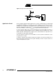
ATAR862-4 Figure 91. FSK Modulation T3R 0 1 2 3 4 0 1 2 3 4 0 1 2 3 4 0 1 2 0 1 2 0 1 2 0 1 2 0 1 2 0 1 2 0 1 2 0 1 2 3 4 0 1 Counter 3 CM31 CM32 SO 0 1 0 T3O Microcontroller Block The microcontroller block is a multichip device which offers a combination of a MARC4based microcontroller and a serial E2PROM data memory in a single package. A microcontroller is used and as serial E2PROM the U505M. Two internal lines can be used as chip-to-chip link in a single package.
Figure 93. Block Diagram EEPROM V DD V SS Timing control HV-generator Address control EEPROM 32 x 16 Mode control SCL I/O control 16-bit read/write buffer 8-bit data register SDA Serial Interface The U505M has a two-wire serial interface (TWI) to the microcontroller for read and write accesses to the EEPROM. The U505M is considered to be a slave in all these applications.
ATAR862-4 Figure 94. MCL Protocol SCL SDA Stand Start by condition Data valid Data/ Data change acknowledge valid Stop Standcondition by • Before the START condition and after the STOP condition the device is in standby mode and the SDA line is switched as input with pull-up resistor. • The control byte that follows the START condition determines the following operation.
Write Operations The EEPROM permits 8-bit and 16-bit write operations. A write access starts with the START condition followed by a write control byte and one or two data bytes from the master. It is completed via the STOP condition from the master after the acknowledge cycle. The programming cycle consists of an erase cycle (write "zeros") and the write cycle (write "ones"). Both cycles together take about 10 ms.
ATAR862-4 read access. If the memory address limit is reached, the data word address will roll over and the sequential read will continue. The master can terminate the read operation after every byte by not responding with an acknowledge (N) and by issuing a stop condition.
Absolute Maximum Ratings Voltages are given relative to VSS Parameters Symbol Value Unit Supply voltage VDD -0.3 to +4.0 V Input voltage (on any pin) VIN VSS -0.3 £ VIN £ VDD +0.
ATAR862-4 DC Operating Characteristics (Continued) VSS = 0 V, Tamb = -40°C to +125°C unless otherwise specified. Parameters Test Conditions Symbol Min. Typ. Max. Unit Power-on Reset Threshold Voltage POR threshold voltage BOT = 1 VPOR 1.6 1.7 1.8 V POR threshold voltage BOT = 0 VPOR 1.85 2.0 2.15 V POR hysteresis 50 VPOR mV Voltage Monitor Threshold Voltage VM high threshold voltage VDD > VM, VMS = 1 VMThh 2.
AC Characteristics Supply Voltage VDD = 2.0 V to 4.0 V, VSS = 0 V, Tamb = 25°C unless otherwise specified. Parameters Test Conditions Symbol Min. VDD = 2.0 V to 4.0 V Tamb = -40°C to +125°C tSYSCL VDD = 2.4 V to 4.0 V Tamb = -40°C to +125°C tSYSCL Typ. Max.
ATAR862-4 AC Characteristics (Continued) Supply Voltage VDD = 2.0 V to 4.0 V, VSS = 0 V, Tamb = 25°C unless otherwise specified. Parameters Test Conditions Symbol Min. Typ. Max. Unit 32-kHz Crystal Oscillator (Operating Range VDD = 2.0 V to 4.0 V) Frequency fX 32.768 kHz Start-up time tSQ 0.
Ordering Information Please select the option settings from the list below and insert ROM CRC.
ATAR862-4 Ordering Information Extended Type Number Package ATAR862M-xxxR4-TNQ Remarks SSO24 429 MHz to 439 MHz Package Information 5.7 5.3 Package SSO24 Dimensions in mm 8.05 7.80 4.5 4.3 1.30 0.15 0.15 0.05 0.25 6.6 6.3 0.65 7.
Table of Contents Features ................................................................................................. 1 Description ............................................................................................ 1 Pin Configuration .................................................................................. 2 Pin Description: RF Part ...................................................................... 2 Pin Description: Microcontroller Part ......................................
ATAR862-4 Return Stack .................................................................................................15 Registers .............................................................................................................16 Program Counter (PC) ..................................................................................16 RAM Address Registers ................................................................................17 Expression Stack Pointer (SP) ..........................
Bi-directional Ports ............................................................................. 33 Bi-directional Port 1 ............................................................................................33 Bi-directional Port 2 ............................................................................................34 Port 2 Data Register (P2DAT) ......................................................................35 Port 2 Control Register (P2CR) ...........................................
ATAR862-4 Timer 3 – Mode 2: Timer/Counter, External Trigger Restart and External Capture (with T3I Input) .....................................................57 Timer 3 – Mode 3: Timer/Counter, Internal Trigger Restart and Internal Capture (with TOG2) .........................................................58 Timer 3 – Mode 4: Timer/Counter .................................................................58 Timer 3 – Mode 5: Timer/Counter, External Trigger Restart and External Capture (with T3I Input) ...
Serial Receive Buffer (SRB) – Byte Read .....................................................76 Combination Modes ........................................................................... 77 Combination Mode Timer 2 and SSI ...................................................................77 Combination Mode 1: Burst Modulation ........................................................78 Combination Mode 2: Biphase Modulation 1 ................................................
ATAR862-4 Thermal Resistance ............................................................................ 94 DC Operating Characteristics ............................................................ 94 AC Characteristics .............................................................................. 96 Crystal Characteristics ....................................................................... 97 Ordering Information ..........................................................................
Atmel Headquarters Atmel Operations Corporate Headquarters Memory 2325 Orchard Parkway San Jose, CA 95131 TEL 1(408) 441-0311 FAX 1(408) 487-2600 Europe Atmel Sarl Route des Arsenaux 41 Case Postale 80 CH-1705 Fribourg Switzerland TEL (41) 26-426-5555 FAX (41) 26-426-5500 Asia Room 1219 Chinachem Golden Plaza 77 Mody Road Tsimhatsui East Kowloon Hong Kong TEL (852) 2721-9778 FAX (852) 2722-1369 Japan 9F, Tonetsu Shinkawa Bldg.