
User guide

1
Features
• Industry-standard Architecture
– Emulates Many 20-pin PALs
®
– Low-cost Easy-to-use Software Tools
• High-speed Electrically-erasable Programmable Logic Devices
– 12 ns Maximum Pin-to-pin Delay
• Low-power - 25 µA Standby Power
• CMOS and TTL Compatible Inputs and Outputs
– Input and I/O Pin Keeper Circuits
• Advanced Flash Technology
– Reprogrammable
– 100% Tested
• High-reliability CMOS Process
– 20 Year Data Retention
– 100 Erase/Write Cycles
– 2,000V ESD Protection
– 200 mA Latchup Immunity
• Commercial and Industrial Temperature Ranges
• Dual-in-line and Surface Mount Packages in Standard Pinouts
• PCI Compliant
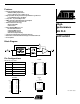
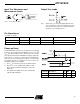
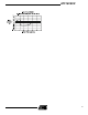
Block Diagram
High-
performance
EE PLD
ATF16V8CZ
Rev. 0453F–08/99
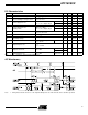
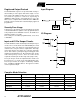
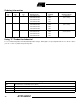
Pin Configurations
All Pinouts Top View
Pin Name Function
CLK Clock
I Logic Inputs
I/O Bidirectional Buffers
OE
Output Enable
VCC +5V Supply
TSSOP
1
2
3
4
5
6
7
8
9
10
20
19
18
17
16
15
14
13
12
11
I/CLK
I1
I2
I3
I4
I5
I6
I7
I8
GND
VCC
I/O
I/O
I/O
I/O
I/O
I/O
I/O
I/O
I9/OE
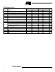
PLCC
4
5
6
7
8
18
17
16
15
14
I3
I4
I5
I6
I7
I/O
I/O
I/O
I/O
I/O
3
2
1
20
19
9
10
11
12
13
I8
GND
I9/OE
I/O
I/O
I2
I1
I/CLK
VCC
I/O
DIP/SOIC
1
2
3
4
5
6
7
8
9
10
20
19
18
17
16
15
14
13
12
11
I/CLK
I1
I2
I3
I4
I5
I6
I7
I8
GND
VCC
I/O
I/O
I/O
I/O
I/O
I/O
I/O
I/O
I9/OE