Features • • • • • • • Next Generation Equivalent of ATF20V8B (ATF20V8BQ, ATF22V10BQC) Complimentary Easy-to-use Atmel-WinCUPL Design Software “Z” Zero Power Compared to “L” Low Power Edge-sensing Zero Standby Power (10 µA Typical) (CQZ) Pin-controlled Zero Standby Power (10 µA Typical) Option (C, CQ) User-controlled Power-down Pin (C, CQ) High-speed Electrically Erasable Programmable Logic Devices – 5 ns Maximum Pin-to-pin Delay (C) • CMOS and TTL Compatible Inputs and Outputs – Pin-keeper Feature Holds I
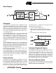
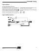
Block Diagram Description The ATF20V8C is a high-performance CMOS (electrically erasable) programmable logic device (PLD) that utilizes Atmel’s proven electrically erasable technology. Speeds down to 5 ns and power dissipation as low as 10 µA are offered. All speed ranges are specified over the full 5V ± 10% range for industrial temperature ranges, and 5V ± 5% for commercial ranges. The ATF20V8C(Q) provides a high-speed CMOS PLD solution with maximum pin-to-pin delay of 5 ns.
ATF20V8C Family Security Fuse Usage Logic data book section titled, “CMOS PLD Programming Hardware and Software Support.” A single fuse is provided to prevent unauthorized copying of the ATF20V8C’s fuse patterns. Once programmed, fuse verify and preload are inhibited. However, the 64-bit User Signature remains accessible. Input and I/O Pull-ups All ATF20V8C family members have internal input and I/O “pin-keeper” circuits.
Functional Logic Diagram Description The logic option and functional diagrams describe the ATF20V8C architecture. Eight configurable macrocells can be configured as a registered output, combinatorial I/O, combinatorial output or dedicated input. operate at high speed. Maximum pin-to-pin delays of 5 ns are offered. Static power loss due to pull-up resistors is eliminated by using input and output pin “keeper” circuits that hold pins to their previous logic levels when idle.
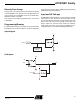
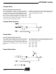
ATF20V8C Family Registered Mode PAL Device Emulation/PAL Replacement The registered mode is used if one or more registers are required. Each macrocell can be configured as either a registered or combinatorial output or I/O, or as an input. For a registered output or I/O, the output is enabled by the OE pin, and the register is clocked by the CLK pin. Eight product terms are allocated to the sum term.
Registered Mode Logic Diagram 6 ATF20V8C Family 0408H–04/01
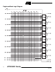
ATF20V8C Family Complex Mode PAL Device Emulation/PAL Replacement In the Complex Mode, combinatorial output and I/O functions are possible. Pins 1 and 11 are regular inputs to the array. Pins 13 through 18 have pin feedback paths back to the AND-array, which makes full I/O capability possible. Pins 12 and 19 (outermost macrocells) are outputs only. They do not have input capability. In this mode, each macrocell has seven product terms going to the sum term and one product term enabling the output.
Complex Mode Logic Diagram 8 ATF20V8C Family 0408H–04/01
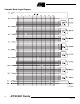
ATF20V8C Family Simple Mode Logic Diagram 9 0408H–04/01
Absolute Maximum Ratings* Temperature under Bias ................................ -55°C to +125°C *NOTICE: Stresses beyond those listed under “Absolute Maximum Ratings” may cause permanent damage to the device. This is a stress rating only and functional operation of the device at these or any other conditions beyond those indicated in the operational sections of this specification is not implied. Exposure to absolute maximum rating conditions for extended periods may affect device reliability.
ATF20V8C Family Input Test Waveforms and Measurement Levels Output Test Loads Commercial tR, tF < 1.5 ns (10% to 90%) Pin Capacitance f = 1 MHz, T = 25°C(1) Typ Max Units Conditions CIN 5 8 pF VIN = 0V COUT 6 8 pF VOUT = 0V Note: 1. Typical values for nominal supply voltage. This parameter is only sampled and is not 100% tested.
ATF20V8C DC Characteristics VCC = 5.0V and TA = 25°C Symbol Parameter Condition IIL Input or I/O Low Leakage Current 0 ≤=VIN ≤=VIL (Max) IIH Input or I/O High Leakage Current 3.5 ≤=VIN ≤=VCC Power Supply Current, Standby ICC Clocked Power Supply Current ICC2 (1) VCC = Max, VIN = Max, Outputs Open VCC = Max, Outputs Open, f = 15 MHz Min Typ Max Units -35 -100 µA 10 µA C-5 Com. 60 90 mA C-5 Ind. 60 100 mA C-7 Com. 60 90 mA C-7 Ind. 60 100 mA C-10 Com.
ATF20V8C AC Waveforms(1) Note: 1. Timing measurement reference is 1.5V. Input AC driving levels are 0.0V and 3.0V, unless otherwise specified. ATF20V8C Family AC Characteristics(1) C-5 C-7 C-10 C-15 Min Max Min Max Min Max Min Max Units 3 5 3 7.5 3 10 3 15 ns 10 ns 8 ns 10 ns Symbol Parameter tPD Input or Feedback to Non-registered Output tCF Clock to Feedback tCO Clock to Output 2 tS Input or Feedback Setup Time 3 5 7.
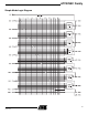
ATF20V8C Characteristic Curves NORMALIZED ICC VS. TEMP 4.5 4.0 3.5 3.0 2.5 2.0 1.5 1.0 0.5 0.0 1.4 NORMALIZED Icc ICC (µA) STAND-BY ICC VS. SUPPLY VOLTAGE (TA = 25°C) TBD 1.2 1.0 TBD 0.8 0.6 0.4 -40.0 4.5 4.8 5.0 5.3 0.0 25.0 75.0 TEMPERATURE (C) 5.5 SUPPLY VOLTAGE (V) SUPPLY CURRENT VS. INPUT FREQUENCY (VCC = 5.0V, TA = 25°C) 140.000 1.000 120.000 I CC (mA) 0.800 100.000 ICC (mA) SUPPLY CURRENT VS. INPUT FREQUENCY (VCC = 5.0V, TA = 25°C) 80.000 TBD 0.600 TBD 0.400 60.000 0.
ATF20V8C ATF20V8C Characteristic Curves (Continued) INPUT CLAMP CURRENT VS. INPUT VOLTAGE (V CC = 5.0V, T A = 35°C) 1 INPUT CURRENT (uA) INPUT CURRENT (mA) 0 -20 -40 TBD -60 -80 -100 -120 0.0 -0.2 -0.4 -0.6 INPUT VOLTAGE (V) INPUT CURRENT VS. INPUT VOLTAGE (VCC = 5.0V, TA = 25°C) -0.8 1 1 TBD 0 0 0 -1.0 0.0 NORMALIZED TPD VS. VCC 6.0 PD PD NORMALIZED T NORMALIZED T 1.1 TBD 1.0 0.9 4.5 4.8 5.0 SUPPLY VOLTAGE (V) 5.3 1.0 TBD 0.9 0.8 -40.0 5.5 NORMALIZED TCO VS. VCC 1.3 0.0 25.
ATF20V8C Characteristic Curves (Continued) DELTA TPD VS. OUTPUT LOADING 6 DELTA T CO (ns) DELTA T PD (ns) 8 4 TBD 2 0 -2 0 50 100 150 200 250 DELTA TCO VS. OUTPUT LOADING 1.00 0.90 0.80 0.70 0.60 0.50 0.40 0.30 0.20 0.10 0.00 300 TBD 50 100 OUTPUT LOADING (PF) DELTA TPD VS. # OF OUTPUT SWITCHING 250 300 DELTA TCO VS. # OF OUTPUT SWITCHING 1.0 DELTA T CO (ns) DELTA T PD (ns) 200 NUMBER OF OUTPUTS LOADING 0.0 -0.1 -0.2 TBD -0.3 -0.4 0.8 0.6 TBD 0.4 0.2 0.0 -0.5 1.0 2.0 3.0 4.
ATF20V8CQ ATF20V8CQ DC Characteristics VCC = 5.0V and TA = 25°C Symbol Parameter Condition IIL Input or I/O Low Leakage Current 0 ≤=VIN ≤=VIL (Max) IIH Input or I/O High Leakage Current 3.5 ≤=VIN ≤=VCC ICC Power Supply Current, Standby VCC = Max, VIN = Max, Outputs Open CQ-10, -15 Com. ICC2 Clocked Power Supply Current VCC = Max, Outputs Open, f = 15 MHz CQ-10, 15 Com. IOS(1) Output Short Circuit Current VOUT = 0.
ATF20V8CQ AC Characteristics(1) CQ-10 Symbol Parameter tPD Input or Feedback to Non-registered Output tCF Clock to Feedback tCO Clock to Output tS Input or Feedback Setup Time tH 8 outputs switching Min Max Units 3 10 ns 1 output switching ns 2 6 ns 7 ns 7.
ATF20V8CQ ATF20V8CQ Characteristic Curves NORMALIZED ICC VS. TEMP 1.4 SUPPLY VOLTAGE (TA = 25°C) 4.5 4.0 3.5 3.0 2.5 2.0 1.5 1.0 0.5 0.0 NORMALIZED Icc ICC (µA) STAND-BY ICC VS. TBD 1.2 1.0 TBD 0.8 0.6 0.4 -40.0 4.5 4.8 5.0 5.3 0.0 25.0 75.0 TEMPERATURE (C) 5.5 SUPPLY VOLTAGE (V) SUPPLY CURRENT VS. INPUT FREQUENCY (VCC = 5.0V, TA = 25°C) SUPPLY CURRENT VS. INPUT FREQUENCY (VCC = 5.0V, TA = 25°C) 140.000 100.000 0.800 I CC (mA) 1.000 ICC (mA) 120.000 80.000 TBD 60.000 0.
ATF20V8CQ Characteristic Curves (Continued) INPUT CLAMP CURRENT VS. INPUT VOLTAGE (V CC = 5.0V, T A = 35°C) 1 INPUT CURRENT (uA) INPUT CURRENT (mA) 0 -20 -40 TBD -60 -80 -100 -120 0.0 -0.2 -0.4 -0.6 INPUT VOLTAGE (V) INPUT CURRENT VS. INPUT VOLTAGE (VCC = 5.0V, TA = 25°C) -0.8 1 1 TBD 0 0 0 -1.0 0.0 NORMALIZED TPD VS. VCC NORMALIZED T TBD 1.0 0.9 4.8 5.0 SUPPLY VOLTAGE (V) 5.3 1.0 TBD 0.9 0.8 -40.0 5.5 NORMALIZED TCO VS. VCC 1.3 0.0 25.0 TEMPERATURE (C) 75.0 NORMALIZED TCO VS.
ATF20V8CQ ATF20V8CQ Characteristic Curves (Continued) DELTA TPD VS. OUTPUT LOADING 6 DELTA T CO (ns) DELTA T PD (ns) 8 4 TBD 2 0 -2 0 50 100 150 200 250 DELTA TCO VS. OUTPUT LOADING 1.00 0.90 0.80 0.70 0.60 0.50 0.40 0.30 0.20 0.10 0.00 300 TBD 50 100 OUTPUT LOADING (PF) 200 250 300 NUMBER OF OUTPUTS LOADING DELTA TPD VS. # OF OUTPUT SWITCHING DELTA TCO VS. # OF OUTPUT SWITCHING 1.0 DELTA T CO (ns) 0.0 DELTA T PD (ns) 150 -0.1 -0.2 TBD -0.3 -0.4 0.8 0.6 TBD 0.4 0.2 0.0 -0.5 1.
ATF20V8CQZ DC Characteristics VCC = 5.0V and TA = 25°C Symbol Parameter Condition IIL Input or I/O Low Leakage Current 0 ≤=VIN ≤=VIL (Max) IIH Input or I/O High Leakage Current 3.5 ≤=VIN ≤=VCC Min ICC Power Supply Current, Standby VCC = Max, VIN = Max, Outputs Open CQZ-15 ICC2 Clocked Power Supply Current VCC = Max, Outputs Open, f = 15 MHz CQZ-15 Typ Max Units -35 -100 µA 10 µA Com. 10 25 µA Ind. 10 50 µA Com. 20 35 mA Ind.
ATF20V8CQZ ATF20V8CQZ AC Characteristics(1) CQZ-15 Min Max Units 3 15 ns 10 ns 8 ns 10 ns Symbol Parameter tPD Input or Feedback to Non-registered Output tCF Clock to Feedback tCO Clock to Output 2 tS Input or Feedback Setup Time 12 ns tH Hold Time 0 ns tP Clock Period 16 ns tW Clock Width 8 ns fMAX 8 outputs switching 1 output switching External Feedback 1/(tS + tCO) 45 MHz Internal Feedback 1/(tS + tCF) 50 MHz No Feedback 1/(tP) 62 MHz tEA Input to Output E
ATF20V8CQZ Characteristic Curves NORMALIZED ICC VS. TEMP 1.4 SUPPLY VOLTAGE (TA = 25°C) 4.5 4.0 3.5 3.0 2.5 2.0 1.5 1.0 0.5 0.0 NORMALIZED Icc ICC (µA) STAND-BY ICC VS. TBD 1.2 1.0 TBD 0.8 0.6 0.4 -40.0 4.5 4.8 5.0 5.3 0.0 25.0 75.0 TEMPERATURE (C) 5.5 SUPPLY VOLTAGE (V) SUPPLY CURRENT VS. INPUT FREQUENCY (VCC = 5.0V, TA = 25°C) 1.000 120.000 0.800 I CC (mA) 140.000 ICC (mA) 100.000 80.000 TBD SUPPLY CURRENT VS. INPUT FREQUENCY (VCC = 5.0V, TA = 25°C) 0.600 TBD 0.400 60.000 0.
ATF20V8CQZ ATF20V8CQZ-15 Characteristic Curves (Continued) INPUT CLAMP CURRENT VS. INPUT VOLTAGE (V CC = 5.0V, T A = 35°C) 1 INPUT CURRENT (uA) INPUT CURRENT (mA) 0 -20 -40 TBD -60 -80 -100 -120 0.0 -0.2 -0.4 -0.6 INPUT VOLTAGE (V) -0.8 INPUT CURRENT VS. INPUT VOLTAGE (VCC = 5.0V, TA = 25°C) 1 1 TBD 0 0 0 -1.0 0.0 NORMALIZED TPD VS. VCC 6.0 PD PD NORMALIZED T NORMALIZED T 1.1 TBD 1.0 0.9 4.5 4.8 5.0 SUPPLY VOLTAGE (V) 5.3 1.0 TBD 0.9 0.8 -40.0 5.5 NORMALIZED TCO VS. VCC 1.3 0.
ATF20V8CQZ-15 Characteristic Curves (Continued) DELTA TPD VS. OUTPUT LOADING 6 DELTA T CO (ns) DELTA T PD (ns) 8 4 TBD 2 0 -2 0 50 100 150 200 250 DELTA TCO VS. OUTPUT LOADING 1.00 0.90 0.80 0.70 0.60 0.50 0.40 0.30 0.20 0.10 0.00 300 TBD 50 100 OUTPUT LOADING (PF) 150 200 250 300 NUMBER OF OUTPUTS LOADING DELTA TCO VS. # OF OUTPUT SWITCHING DELTA TPD VS. # OF OUTPUT SWITCHING 1.0 DELTA T CO (ns) DELTA T PD (ns) 0.0 -0.1 -0.2 TBD -0.3 -0.4 0.8 0.6 TBD 0.4 0.2 0.0 1.0 -0.5 1.
ATF20V8C Family ATF20V8C Family Ordering Information tPD (ns) tS (ns) tCO (ns) Ordering Code Package 5 3 4 ATF20V8C-5JC 28J Commercial (0°C to 70°C) 7.5 3.5 4.
Using “C” Product for Industrial To use commercial product for industrial temperature ranges, down-grade one speed grade from the “I” to the “C” device (7 ns “C” = 10 ns “I”) and de-rate power by 30%. Package Type 28J 28-lead, Plastic J-leaded Chip Carrier (PLCC) 24P3 24-lead, 0.300" Wide, Plastic Dual Inline Package (PDIP) 24S 24-lead, 0.300" Wide, Plastic Gull Wing Small Outline (SOIC) 24X 24-lead, 4.
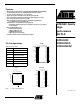
ATF20V8C Family Packaging Information 28J, 28-lead, Plastic J-leaded Chip Carrier (PLCC) Dimensions in Inches and (Millimeters) JEDEC STANDARD MS-018 AB 24P3, 24-lead, 0.300" Wide, Plastic Dual Inline Package (PDIP) Dimensions in Inches and (Millimeters) JEDEC STANDARD MS-001 AF .045(1.14) X 45° PIN NO. 1 IDENTIFY .045(1.14) X 30° - 45° .456(11.6) SQ .450(11.4) .032(.813) .026(.660) .495(12.6) SQ .485(12.3) .050(1.27) TYP .300(7.62) REF SQ 1.27(32.3) 1.25(31.7) PIN 1 .012(.305) .008(.203) .266(6.
Atmel Headquarters Atmel Operations Corporate Headquarters Atmel Colorado Springs 2325 Orchard Parkway San Jose, CA 95131 TEL (408) 441-0311 FAX (408) 487-2600 Europe 1150 E. Cheyenne Mtn. Blvd. Colorado Springs, CO 80906 TEL (719) 576-3300 FAX (719) 540-1759 Atmel Rousset Atmel SarL Route des Arsenaux 41 Casa Postale 80 CH-1705 Fribourg Switzerland TEL (41) 26-426-5555 FAX (41) 26-426-5500 Asia Atmel Asia, Ltd.