
Manual
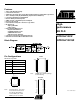
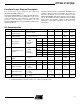
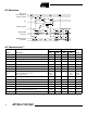
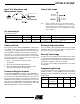

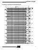

Table Of Contents
- Pin Configurations
- Features
- Block Diagram
- Description
- Absolute Maximum Ratings*
- DC and AC Operating Conditions
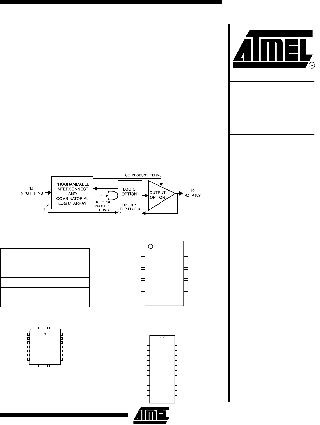
- Functional Logic Diagram Description
- DC Characteristics
- AC Waveforms
- AC Characteristics(1)
- Input Test Waveforms and Measurement Levels
- Output Test Loads
- Pin Capacitance
- Power-up Reset
- Preload of Register Outputs
- Electronic Signature Word
- Security Fuse Usage
- Programming/Erasing
- Input and I/O Pin Keepers
- Functional Logic Diagram ATF22LV10CZ/CQZ
- Ordering Information
- Using “C” Product for Industrial
1
Features
• 3.0V to 5.5V Operating Range
• Lowest Power in It Class
• Advanced Low-voltage, Zero-power, Electrically Erasable Programmable Logic Device
• “Zero” Standby Power (25 µA Maximum) (Input Transition Detection)
• Low-voltage Equivalent of ATF22V10CZ
• Ideal for Battery Powered Systems
• CMOS- and TTL-compatible Inputs and Outputs
• Inputs are 5V Tolerant
• Latch Feature Hold Inputs to Previous Logic States
• EE Technology
– Reprogrammable
– 100% Tested
• High-reliability CMOS Process
– 20-year Data Retention
– 10,000 Erase/Write Cycles
– 2,000V ESD Protection
– 200 mA Latch-up Immunity
• Commercial and Industrial Temperature Ranges
• Dual Inline and Surface Mount Standard Pinouts
Block Diagram
High-
performance
EE PLD
ATF22LV10CZ
ATF22LV10CQZ
Rev. 0779K–04/01
Pin Configurations
All Pinouts Top View
Pin Name Function
CLK Clock
IN Logic Inputs
I/O Bi-directional Buffers
GND Ground
VCC (3 to 5.5V) Supply
TSSOP
Note: TSSOP is the smallest package
of SPLD offering.
1
2
3
4
5
6
7
8
9
10
11
12
24
23
22
21
20
19
18
17
16
15
14
13
CLK/IN
IN
IN
IN
IN
IN
IN
IN
IN
IN
IN
GND
VCC
I/O
I/O
I/O
I/O
I/O
I/O
I/O
I/O
I/O
I/O
IN
DIP/SOIC
1
2
3
4
5
6
7
8
9
10
11
12
24
23
22
21
20
19
18
17
16
15
14
13
CLK/IN
IN
IN
IN
IN
IN
IN
IN
IN
IN
IN
GND
VCC
I/O
I/O
I/O
I/O
I/O
I/O
I/O
I/O
I/O
I/O
IN
PLCC
Note: For PLCC, pins 1, 8, 15, and
22 can be left unconnected.
For superior performance,
connect VCC to pin 1 and
GND to pins 8, 15, and 22.
5
6
7
8
9
10
11
25
24
23
22
21
20
19
IN
IN
IN
GND*
IN
IN
IN
I/O
I/O
I/O
GND*
I/O
I/O
I/O
4
3
2
1
28
27
26
12
13
14
15
16
17
18
IN
IN
GND
GND*
IN
I/O
I/O
IN
IN
CLK/IN
VCC*
VCC
I/O
I/O