
User guide


1
Features
• Industry-standard Architecture
• 12 ns Maximum Pin-to-pin Delay
• Zero Power – 25 µA Maximum Standby Power (Input Transition Detection)
• CMOS and TTL Compatible Inputs and Outputs
• Advanced Electrically-erasableTechnology
– Reprogrammable
– 100% Tested
• Latch Feature Holds Inputs to Previous Logic State
• High-reliability CMOS Process
– 20 Year Data Retention
– 100 Erase/Write Cycles
– 2,000V ESD Protection
– 200 mA Latchup Immunity
• Commercial and Industrial Temperature Ranges
• Dual-in-line and Surface Mount Standard Pinouts
• PCI Compliant
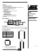
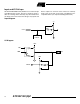
Block Diagram
Description
The ATF22V10CZ/CQZ is a high-performance CMOS (electrically-erasable)
programmable logic device (PLD) which utilizes Atmel’s proven electrically-erasable
High-
performance
EE PLD
ATF22V10CZ
ATF22V10CQZ
Rev. 0778H–03/01
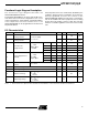
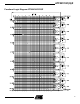
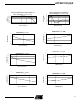
Pin Configurations
All Pinouts Top View
Pin Name Function
CLK Clock
IN Logic Inputs
I/O Bi-directional Buffers
VCC +5V Supply
TSSOP
1
2
3
4
5
6
7
8
9
10
11
12
24
23
22
21
20
19
18
17
16
15
14
13
CLK/IN
IN
IN
IN
IN
IN
IN
IN
IN
IN
IN
GND
VCC
I/O
I/O
I/O
I/O
I/O
I/O
I/O
I/O
I/O
I/O
IN
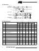
PLCC
5
6
7
8
9
10
11
25
24
23
22
21
20
19
IN
IN
IN
GND*
IN
IN
IN
I/O
I/O
I/O
GND*
I/O
I/O
I/O
4
3
2
1
28
27
26
12
13
14
15
16
17
18
IN
IN
GND
GND*
IN
I/O
I/O
IN
IN
CLK/IN
VCC*
VCC
I/O
I/O
DIP/SOIC
1
2
3
4
5
6
7
8
9
10
11
12
24
23
22
21
20
19
18
17
16
15
14
13
CLK/IN
IN
IN
IN
IN
IN
IN
IN
IN
IN
IN
GND
VCC
I/O
I/O
I/O
I/O
I/O
I/O
I/O
I/O
I/O
I/O
IN
Note: For PLCC, P1, P8, P15 and P22 can be left
unconnected. For superior performance, con-
nect VCC to pin 1 and GND to 8, 15, and 22.
(continued)