
Manual


5
4925A–GPS–02/06
ATR0625 [Preliminary]
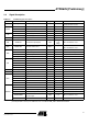
3. Pin Configuration
3.1 Pinout
Figure 3-1. Pinout QFN56 (Top View)
42 29
114
43 28
56 15
ATR0625
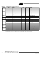
Table 3-1. ATR0625 Pinout
Pin Name QFN56
Pin
Type
Pull Resistor
(Reset Value)
(1)
Firmware Label
PIO Bank A PIO Bank B
IOIO
CLK23 37 IN
DBG_EN 8 IN PD
GND
(2)
IN
LDOBAT_IN 21 IN
LDO_EN 25 IN
LDO_IN 20 IN
LDO_OUT 19 OUT
NRESET 41 I/O Open Drain PU
NSHDN 26 OUT
NSLEEP 24 OUT
NTRST 13 IN PD
P0 40 I/O PD NANTSHORT
P1 47 I/O Configurable (PD) GPSMODE0 AGCOUT1
P2 46 I/O Configurable (PD) BOOT_MODE “0”
P8 48 I/O Configurable (PD) STATUSLED “0”
P9 29 I/O PU EXTINT0 EXTINT0
P12 49 I/O Configurable (PU) GPSMODE2 NPCS2
P13 32 I/O PU GPSMODE3 EXTINT1
Notes: 1. PD = internal pull-down resistor, PU = internal pull-up resistor, OH = switched to Output High at reset
2. Ground plane
3. VBAT18 represent the internal power supply of the backup power domain, see section “Power Supply” on page 17.
4. VDDIO is the supply voltage for the following GPIO-pins: P1, P2, P8, P12, P14, P16, P17, P18, P19, P20, P21, P23, P24,
P25, P26, P27 and P29, see section “Power Supply” on page 17.
5. VDD_USB is the supply voltage for following the USB-pins: USB_DM and USB_DP, see section “Power Supply” on page
17. For operation of the USB interface, supply of 3.0V to 3.6V is required.
6. This pin is not connected