Features • 16-channel GPS Correlator • • • • • • • • • • • • • • • • – 8192 Search Bins with GPS Acquisition Accelerator – Accuracy: 2.
1. Description The ATR0635P1 is a low-power, single-chip GPS receiver, especially designed to meet the requirements of mobile applications. It is based on Atmel®’s ANTARIS®4 technology and integrates an RF front-end, filtering, and a baseband processor in a single, tiny 7 mm × 10 mm 96 pin BGA package. Providing excellent RF performance with low noise figure and low power consumption.
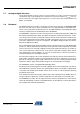
ATR0635P1 2. Architectural Overview 2.1 Block Diagram Figure 2-1.
2.2 General Description The ATR0635P1 has been designed especially for mobile applications. It provides high isolation between GPS and cellular bands, as well as very low power consumption. ATR0635P1 is based on the successful ANTARIS4 technology which includes the ANTARIS high performance SuperSense software in ROM, developed by u-blox AG, Switzerland.
ATR0635P1 2.7 Analog-to-digital Converter The analog-to-digital converter stage has a total resolution of 1.5 bits. It comprises balanced comparators and a sub-sampling unit, clocked by the reference frequency (fTCXO). The frequency spectrum of the digital output signal (f OUT ), present at the data outputs SIGLO and SIGH1, is 4.348 MHz. 2.8 Baseband The GPS baseband core includes a 16-channel correlator and is based on an ARM7TDMI ARM processor core with very low power consumption.
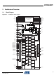
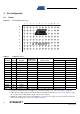
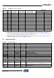
3. Pin Configuration 3.1 Pinout Figure 3-1. Pinning BGA96 (Top View) 1 2 3 4 5 6 7 8 9 10 11 12 A B C D E F G ATR0635P1 H Table 3-1.
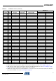
ATR0635P1 Table 3-1.
Table 3-1.
ATR0635P1 Table 3-1. Pin Name ATR0635P1 Pinout (Continued) BGA 96 (3) VDD_USB Pin Type A10 Supply VDD18 H9 Supply VDD18 G11 Supply VDD18 F12 Supply VDD18 B9 Supply VDD18 E5 Supply B5 Supply VDDIO H5 Supply VDIG A5 Supply X A2 Analog OUT XT_IN A12 Analog IN XT_OUT B12 Analog OUT XTO A1 Analog Input VDDIO Notes: (4) Pull Resistor (Reset Value)(1) PIO Bank A Firmware Label I O 1.
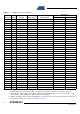
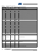
Table 3-2.
ATR0635P1 Table 3-2.
3.3 Setting GPSMODE0 to GPSMODE12 The start-up configuration of this ROM-based system without external non-volatile memory is defined by the status of the GPSMODE pins after system reset. Alternatively, the system can be configured through message commands passed through the serial interface after start-up. This configuration of the ATR0635P1 can be stored in an external non-volatile memory like EEPROM. Default designates settings used by ROM firmware if GPSMODE configuration is disabled (GPSMODE0 = 0).
ATR0635P1 3.3.2 Sensitivity Settings Table 3-5. GPSMODE3 (Fixed PU) 0(1) (1) GPSMODE2 (Reset = PU) Description 0 Auto mode (Default ROM value) (2) Fast mode 0 Normal mode 1 0 (2) 1 1(2) Notes: GPS Sensitivity Settings 1(2) High sensitivity 1. Increased back-up current 2. Leave open For all GPS receivers the sensitivity depends on the integration time of the GPS signals. Therefore there is a trade-off between sensitivity and the time to detect the GPS signal (Time to first fix).
Both USART ports accept input messages in all three supported protocols (NMEA, RTCM and UBX) at the configured baud rate. Input messages of all three protocols can be arbitrarily mixed. Response to a query input message will always use the same protocol as the query input message. The USB port does only accept NMEA and UBX as input protocol by default. RTCM can be enabled via protocol messages on demand.
ATR0635P1 The following settings apply if GPSMODE configuration is not enabled, that is, GPSMODE = 0 (ROM defaults): Table 3-11. Serial I/O Default Setting if GPSMODE Configuration is Deselected (GPSMODE0 = 0) USB NMEA USART1 NMEA Baud rate (kBaud) 57.6 57.
Table 3-13.
ATR0635P1 3.4.3 External Connections for a Working GPS System Figure 3-2. Example of an External Connection (ATR0635P1) ATR0635P1 LNA (optional) SAW NC NC NC SIGHI SIGLO CLK23 RF NRF ATR0610 RF_ON PURF NSLEEP PUXTO NC NC NC NC NC NC NC see Table 3-15 see Table 3-15 see Table 3-15 see Table 3-15 see Table 3-15 see Table 3-15 NRESET TMS TCK TDI NTRST TDO DBG_EN P0 - 2 P9 P12 - 17 P19 P23 - 27 P29 - 30 P30/AGCOUT0 SDI NC NC GND analog MO TEST EGC XT_IN 32.768 kHz (see RTC) XT_OUT XTO TCXO 23.
Table 3-15. Recommended Pin Connections Pin Name Recommended External Circuit P0/NANTSHORT Internal pull-down resistor; leave open if Antenna Supervision functionality is unused. P1/GPSMODE0 Internal pull-down resistor; leave open in order to disable the GPSMODE pin configuration feature. Connect to VDD18 to enable the GPSMODE pin configuration feature. Refer to GPSMODE definitions in “Setting GPSMODE0 to GPSMODE12” on page 12. P2/BOOT_MODE Internal pull-down resistor; leave open.
ATR0635P1 3.5 Connecting an Optional Serial EEPROM The ATR0635P1 offers the possibility of connecting an external serial EEPROM. The internal ROM firmware supports storing the configuration of the ATR0635P1 in serial EEPROM. The pin P16/NEEPROM signals the firmware that a serial EEPROM is connected to the ATR0635P1. The ATR0635P1’s 32-bit RISC processor accesses the external memory via SPI (serial peripheral interface). For best results, use a 32-Kbit 1.8V serial EEPROM such as Atmel’s AT25320AY1-1.8.
4. Power Supply The ATR0635P1 is supplied with six distinct supply voltages: • The power supplies for the RF part (VCC1, VCC2, VBP) within 2.7V to 3.3V. • VDIG, the 1.8V supply of the digital pins of the RF part (SIGHI, SIGLO and CLK23). VDIG should be connected to VDD18. • VDD18, the nominal 1.8V supply voltage for the core, the I/O pins, the memory interface and the test pins and all GPIO pins not mentioned in next item. • VDDIO, the variable supply voltage within 1.8V to 3.
ATR0635P1 Figure 4-1. Connecting Example: Separate Power Supplies for RF and Digital Part Using the Internal LDOs ATR0635P1 internal VCC1 2.7V to 3.3V VCC2 RF VBP VDIG 2.3V to 3.6V LDO_IN NSHDN LDO_EN LDO_OUT LDO18 ldoin ldoen ldoout VDD18 Core VDDIO 1.8V to 3.3V variable I/O domain 1 µF (X7R) ldobat_in LDOBAT LDOBAT_IN 1.5V to 3.6V VBAT VBAT18 vbat vbat18 VDD 1 µF (X7R) RTC backup memory 0V or 3V to 3.
The RTC section will be initialized properly if VDD18 is supplied first to the ATR0635P1. If VBAT is applied first, the current consumption of the RTC and backup SRAM is undetermined. Figure 4-2. Connecting Example: Common Power Supplies for RF and Digital Part Using the Internal LDOs ATR0635P1 internal VCC1 2.7V to 3.3V VCC2 RF VBP VDIG 2.3V to 3.6V LDO_IN NSHDN LDO_EN LDO_OUT LDO18 ldoin ldoen ldoout VDD18 Core VDDIO 1.8V to 3.3V variable I/O domain 1 µF (X7R) ldobat_in LDOBAT LDOBAT_IN 1.
ATR0635P1 Figure 4-3. Connecting Example: Separate Power Supplies for RF and Digital Part Using 1.8V from Host System ATR0635P1 internal VCC1 2.7V to 3.3V VCC2 RF VBP VDIG LDO_IN LDO_EN LDO_OUT LDO18 ldoin ldoen ldoout 1.65V to 1.95V VDD18 Core VDDIO 1.8V to 3.3V variable I/O domain 1 µF (X7R) ldobat_in 2.3V to 3.6V LDOBAT_IN 1.5V to 3.6V VBAT VBAT18 LDOBAT vbat vbat18 VDD 1 µF (X7R) RTC backup memory 0V or 3V to 3.
Figure 4-4. Connecting Example: Power Supply from USB Using the Internal LDOs ATR0635P1 internal VCC1 VCC2 RF VBP VDIG LDO_IN NSHDN LDO_EN LDO_OUT LDO18 ldoin ldoen ldoout VDD18 Core VDDIO 1.8V to 3.3V variable I/O domain 1 µF (X7R) ldobat_in LDOBAT LDOBAT_IN 1.5V to 3.6V VBAT VBAT18 vbat vbat18 VDD 1 µF (X7R) RTC backup memory USB-VSB 5V 24 External LDO 3.0V to 3.
ATR0635P1 5. Crystals The ATR0635P1 requires a GPS TCXO. The reference frequency is 23.104 MHz. By connecting an optional RTC crystal, different power modes are available. The reference frequency is 32.768 kHz. 5.1 GPS Figure 5-1. Equivalent Application Examples Using a GPS TCXO (See Table 5-1 on page 26) 22 pF A1 XTO 12 pF B3 TCXO 4.7 pF NXTO A2 Do not connect X B2 NX A1 12 pF XTO 22 pF B3 TCXO 4.7 pF A2 Do not connect NXTO X B2 NX Figure 5-2.
Table 5-1. Specification of GPS TCXOs Appropriate for the Application Example Shown in Figure 5-1 on page 25 Parameter Comment Min Typ Max Units Frequency Characteristics Nominal frequency referenced to 25°C Nominal Frequency 23.104 MHz Over operating temperature range 0.5 ±ppm Frequency deviation Including calibration, temperature, soldering and ageing effects 8 ±ppm Temperature range Operating temperature range –40.0 +85.0 °C 1.
ATR0635P1 6. Absolute Maximum Ratings Stresses beyond those listed under “Absolute Maximum Ratings” may cause permanent damage to the device. This is a stress rating only and functional operation of the device at these or any other conditions beyond those indicated in the operational sections of this specification is not implied. Exposure to absolute maximum rating conditions for extended periods may affect device reliability.
9. Operating Range Parameters Pins Symbol Min Analog supply voltage RF VCC1, VCC2, VBP VCC 2.70 Digital supply voltage RF VDIG VDIG 1.65 Digital supply voltage core VDD18 VDD18 Digital supply voltage VDDIO domain(1) VDDIO Digital supply voltage USB(2) DC supply voltage LDO18 DC supply voltage LDOBAT DC Supply voltage VBAT Max Unit 3.30 V 1.8 1.95 V 1.65 1.8 1.95 V VDDIO 1.65 1.8/3.3 3.6 V VDD_USB VDD_USB 3.0 3.3 3.6 V LDO_IN LDO_IN 2.3 3.
ATR0635P1 10. Electrical Characteristics (Continued) If no additional information is given in column Test Conditions, the values apply to temperature range from –40°C to +85°C. No. Parameters Test Conditions Pin Symbol 2.4 AGC cut-off frequency Cext = open A4 f3dB_AGC 2.5 AGC cut-off frequency Cext = 100 pF A4 f3dB_AGC Unit Type* 250 kHz D 33 kHz D 3.1 Voltage level power-on F4, G4, H4 VPU,on V A 3.2 Voltage level power-off F4, G4, H4 VPU,off 0.5 V A 1.
10. Electrical Characteristics (Continued) If no additional information is given in column Test Conditions, the values apply to temperature range from –40°C to +85°C. No. Parameters Test Conditions 6.7 Schmitt trigger hysteresis VDD18 = 1.65V to 1.95V Pin Symbol Min CLK23 Vhyst,CLK23 Typ Max Unit Type* 0.2 0.55 V C 6.8 Schmitt trigger threshold rising VDD18 = 1.65V to 1.95V NRESET Vth+,NRESET 0.8 1.3 V C 6.9 Schmitt trigger threshold falling VDD18 = 1.65V to 1.
ATR0635P1 10. Electrical Characteristics (Continued) If no additional information is given in column Test Conditions, the values apply to temperature range from –40°C to +85°C. No. Parameters Test Conditions Pin Symbol Min A7 RPU Typ Max Unit Type* 0.5 1.8 kΩ A 6.26 Input pull-up resistor NRESET 6.27 Input pull-up resistors TCK, TDI, TMS G9, H10, G10 RPU 7 18 kΩ A 6.28 Input pull-up resistors P9, P13, P22, P31 A11, B10, C10, D10 RPU 100 235 kΩ A 6.
11. Power Consumption Table 11-1. Leakage Currents Parameter Conditions Typ. Max. Unit Type* Leakage current VDD18 VDD18 = 1.95V, no currents across pull-up resistors, PLL disabled 10 200 µA A Leakage current VDDIO VDDIO = 1.95V no currents across pull-up resistors 2 5 µA A 7 20 µA A Leakage current LDOBAT No currents across pull-up + backup domain resistors *) Type means: A = 100% tested, B = 100% correlation tested, C = Characterized on samples, D = Design parameter Table 11-2.
ATR0635P1 12. Ordering Information Extended Type Number Package MPQ Remarks ATR0635P1-7KQY BGA96 3000 7 mm × 10 mm, 0.8 mm pitch, Pb-free, RoHS-compliant ATR0635-EK1 - 1 Evaluation kit/Road test kit ATR0635-DK1 - 1 Design kit including design guide and PCB Gerber files 13. Package Information Package: BGA96 Dimensions in mm n 0.08 m n 0.15 m 2. C BA 0.4±0.05 A1 Corner Top View Bottom View A1 Corner A B C D E F G H 0.8 7±0.05 0.8 Pin A1 Laser Marking A 8.8 10±0.
14. Revision History Please note that the following page numbers referred to in this section refer to the specific revision mentioned, not to this document. 34 Revision No. History 4979D-GPS-06/08 • Section 8 “Thermal Resistance” on page 27 added • Section 10 “Electrical Characteristics” numbers 2.6 and 2.7 on page 29 deleted • Section 10 “Electrical Characteristics” numbers 4.2, 6.7 and 6.26 to 6.
Headquarters International Atmel Corporation 2325 Orchard Parkway San Jose, CA 95131 USA Tel: 1(408) 441-0311 Fax: 1(408) 487-2600 Atmel Asia Room 1219 Chinachem Golden Plaza 77 Mody Road Tsimshatsui East Kowloon Hong Kong Tel: (852) 2721-9778 Fax: (852) 2722-1369 Atmel Europe Le Krebs 8, Rue Jean-Pierre Timbaud BP 309 78054 Saint-Quentin-en-Yvelines Cedex France Tel: (33) 1-30-60-70-00 Fax: (33) 1-30-60-71-11 Atmel Japan 9F, Tonetsu Shinkawa Bldg.