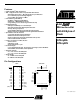
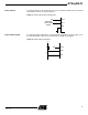
Features • Utilizes the AVR® RISC Architecture • AVR – High-performance and Low-power RISC Architecture • • • • • • • – 90 Powerful Instructions – Most Single Clock Cycle Execution – 32 x 8 General-purpose Working Registers – Up to 4 MIPS Throughput at 4 MHz Nonvolatile Program Memory – 2K Bytes of Flash Program Memory – Endurance: 1,000 Write/Erase Cycles – Programming Lock for Flash Program Data Security Peripheral Features – Interrupt and Wake-up on Low-level Input – One 8-bit Timer/Counter with Se
Description The ATtiny28 is a low-power CMOS 8-bit microcontroller based on the AVR RISC architecture. By executing powerful instructions in a single clock cycle, the ATtiny28 achieves throughputs approaching 1 MIPS per MHz, allowing the system designer to optimize power consumption versus processing speed. The AVR core combines a rich instruction set with 32 general-purpose working registers.
ATtiny28L/V rupt on low-level input feature enables the ATtiny28 to be highly responsive to external events, still featuring the lowest power consumption while in the power-down modes. The device is manufactured using Atmel’s high-density, nonvolatile memory technology. By combining an enhanced RISC 8-bit CPU with Flash on a monolithic chip, the Atmel ATtiny28 is a powerful microcontroller that provides a highly flexible and cost-effective solution to many embedded control applications.
Clock Options The device has the following clock source options, selectable by Flash Fuse bits as shown in Table 1. Table 1. Device Clocking Option Select Clock Option CKSEL3..0 External Crystal/Ceramic Resonator 1111 - 1010 External Low-frequency Crystal 1001 - 1000 External RC Oscillator 0111 - 0101 Internal RC Oscillator 0100 - 0010 External Clock 0001 - 0000 Note: “1” means unprogrammed, “0” means programmed.
ATtiny28L/V External Clock To drive the device from an external clock source, XTAL2 should be left unconnected while XTAL1 is driven as shown in Figure 3. Figure 3. External Clock Drive Configuration NC XTAL2 EXTERNAL OSCILLATOR SIGNAL XTAL1 GND External RC Oscillator For timing insensitive applications, the external RC configuration shown in Figure 4 can be used. For details on how to choose R and C, see Table 25 on page 54. Figure 4.
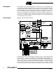
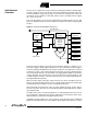
Architectural Overview The fast-access register file concept contains 32 x 8-bit general-purpose working registers with a single clock cycle access time. This means that during one single clock cycle, one ALU (Arithmetic Logic Unit) operation is executed. Two operands are output from the register file, the operation is executed, and the result is stored back in the register file – in one clock cycle. Two of the 32 registers can be used as a 16-bit pointer for indirect memory access.
ATtiny28L/V r a te i nt er r up t v e c to r i n t h e i n te r r u pt v ec t or t a bl e at th e b e gi n ni n g of th e program memory. The different interrupts have priority in accordance with their interrupt vector position. The lower the interrupt vector address, the higher the priority. General-purpose Register File Figure 6 shows the structure of the 32 general-purpose registers in the CPU. Figure 6.
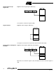
Register Direct, Single Register Rd Figure 7. Direct Single Register Addressing The operand is contained in register d (Rd). Register Indirect Figure 8. Indirect Register Addressing REGISTERFILE 0 Z-Register 30 31 The register accessed is the one pointed to by the Z-register (R31, R30). Register Direct, Two Registers Rd and Rr Figure 9. Direct Register Addressing, Two Registers Operands are contained in register r (Rr) and d (Rd). The result is stored in register d (Rd).
ATtiny28L/V I/O Direct Figure 10. I/O Direct Addressing Operand address is contained in six bits of the instruction word. n is the destination or source register address. Relative Program Addressing, RJMP and RCALL Figure 11. Relative Program Memory Addressing PROGRAM MEMORY 15 $000 0 PC +1 15 12 11 OP 0 k $3FF Program execution continues at address PC + k + 1. The relative address k is -2048 to 2047. Constant Addressing Using the LPM Instruction Figure 12.
Subroutine and Interrupt Hardware Stack The ATtiny28 uses a 3-level-deep hardware stack for subroutines and interrupts. The hardware stack is 10 bits wide and stores the program counter (PC) return address while subroutines and interrupts are executed. RCALL instructions and interrupts push the PC return address onto stack level 0, and the data in the other stack levels 1 - 2 are pushed one level deeper in the stack.
ATtiny28L/V I/O Memory The I/O space definition of the ATtiny28 is shown in Table 2. Table 2.
an interrupt has occurred, and is set by the RETI instruction to enable subsequent interrupts. • Bit 6 – T: Bit Copy Storage The bit copy instructions BLD (Bit LoaD) and BST (Bit STore) use the T-bit as source and destination for the operated bit. A bit from a register in the register file can be copied into T by the BST instruction, and a bit in T can be copied into a bit in a register in the register file by the BLD instruction.
ATtiny28L/V Table 3. Reset and Interrupt Vectors Vector No.
Figure 15. Reset Logic DATA BUS 100 - 500K RESET Reset Circuit Watchdog Timer CKSEL[3..0] On-chip RC Oscillator S COUNTER RESET Power-on Reset Circuit VCC Q INTERNAL RESET PORF EXTRF WDRF MCU Control and Status Register (MCUCS) R Delay Counters Full CK Table 4. Reset Characteristics Symbol VPOT(1) VRST Note: Parameter Min Typ Max Unit Power-on Reset Threshold Voltage (rising) 1.0 1.4 1.8 V Power-on Reset Threshold Voltage (falling) 0.4 0.6 0.
ATtiny28L/V Table 5. ATtiny28 Clock Options and Start-up Time (Continued) CKSEL3..0 Note: Clock Source Start-up Time at 2.7V 0100 Internal RC Oscillator 6 CK 0011 Internal RC Oscillator 4.2 ms + 6 CK 0010 Internal RC Oscillator 67 ms + 6 CK 0001 External Clock 6 CK 0000 External Clock 4.2 ms + 6 CK 1. Due to limited number of clock cycles in the start-up period, it is recommended that ceramic resonator be used. This table shows the start-up times from reset.
Figure 16. MCU Start-up, RESET Tied to VCC. VCC RESET VPOT VRST tTOUT TIME-OUT INTERNAL RESET Figure 17. MCU Start-up, RESET Controlled Externally VCC VPOT VRST RESET tTOUT TIME-OUT INTERNAL RESET External Reset An external reset is generated by a low level on the RESET pin. Reset pulses longer than 50 ns will generate a reset, even if the clock is not running. Shorter pulses are not guaranteed to generate a reset.
ATtiny28L/V Watchdog Reset When the Watchdog times out, it will generate a short reset pulse of 1 XTAL cycle duration. On the falling edge of this pulse, the delay timer starts counting the Time-out period (tTOUT). Refer to page 26 for details on operation of the Watchdog. Figure 19. Watchdog Reset during Operation MCU Control and Status Register – MCUCS The MCU Control and Status Register contains control and status bits for general MCU functions.
• Bit 1 – EXTRF: External Reset Flag This bit is set if an external reset occurs. The bit is cleared by a Power-on Reset, or by writing a logical “0” to the flag. • Bit 0 – PORF: Power-on Reset Flag This bit is set if a Power-on Reset occurs. The bit is cleared by writing a logical “0” to the flag. To make use of the reset flags to identify a reset condition, the user should read and then clear the flag bits in MCUCS as early as possible in the program.
ATtiny28L/V Interrupt Control Register – ICR Bit 7 6 5 4 3 2 1 0 $06 INT1 INT0 LLIE TOIE0 ISC11 ISC10 ISC01 ISC00 Read/Write R/W R/W R/W R/W R/W R/W R/W R/W Initial Value 0 0 0 0 0 0 0 0 ICR • Bit 7 – INT1: External Interrupt Request 1 Enable When the INT1 bit is set (one) and I-bit in the Status Register (SREG) is set (one), the external pin interrupt 1 is enabled.
Table 7. Interrupt 1 Sense Control ISC11 ISC10 0 0 The low level of INT1 generates an interrupt request. 0 1 Any change on INT1 generates an interrupt request. 1 0 The falling edge of INT1 generates an interrupt request. 1 1 The rising edge of INT1 generates an interrupt request. Note: Description When changing the ISC11/ISC10 bits, INT1 must be disabled by clearing its Interrupt Enable bit. Otherwise, an interrupt can occur when the bits are changed.
ATtiny28L/V cleared by writing a logical “1” to it. This flag is always cleared when INT0 is configured as level interrupt. • Bit 5 – Res: Reserved Bit This bit is a reserved bit in the ATtiny28 and always reads as zero. • Bit 4 – TOV0: Timer/Counter0 Overflow Flag The bit TOV0 is set (one) when an overflow occurs in Timer/Counter0. TOV0 is cleared by hardware when executing the corresponding interrupt handling vector. TOV0 is cleared by writing a logical “1” to the flag.
Power-down Mode When the SM bit is set (one), the SLEEP instruction forces the MCU into the Powerdown mode. In this mode, the external oscillator is stopped, while the external interrupts and the Watchdog (if enabled) continue operating. Only an external reset, a Watchdog reset (if enabled), or an external level interrupt can wake up the MCU. Note that if a level-triggered interrupt is used for wake-up from Power-down mode, the changed level must be held for some time to wake up the MCU.
ATtiny28L/V Timer/Counter0 The ATtiny28 provides one general-purpose 8-bit Timer/Counter – Timer/Counter0. Timer/Counter0 has prescaling selection from the 10-bit prescaling timer. The Timer/Counter0 can either be used as a timer with an internal clock time base or as a counter with an external pin connection that triggers the counting. Timer/Counter Prescaler Figure 20 shows the Timer/Counter prescaler. Figure 20.
The 8-bit Timer/Counter0 can select clock source from CK, prescaled CK or an external pin. In addition, it can be stopped as described in the specification for the Timer/Counter0 Control Register (TCCR0). The overflow status flag is found in the Interrupt Flag Register (IFR). Control signals are found in the Timer/Counter0 Control Register (TCCR0). The interrupt enable/disable setting for Timer/Counter0 is found in the Interrupt Control Register (ICR).
ATtiny28L/V Table 10. Clock 0 Prescale Select CS02 CS01 CS00 Description 0 0 0 Stop, the Timer/Counter0 is stopped. 0 0 1 CK 0 1 0 Modulator Period 0 1 1 CK/64 1 0 0 CK/256 1 0 1 CK/1024 1 1 0 External Pin T0, falling edge 1 1 1 External Pin T0, rising edge The Stop condition provides a Timer Enable/Disable function. The CK down divided modes are scaled directly from the CK oscillator clock.
Watchdog Timer The Watchdog Timer is clocked from a separate on-chip oscillator. By controlling the Watchdog Timer prescaler, the Watchdog reset interval can be adjusted as shown in Table 11. See characterization data for typical values at other VCC levels. The WDR (Watchdog Reset) instruction resets the Watchdog Timer. Eight different clock cycle periods can be selected to determine the reset period.
ATtiny28L/V • Bits 2..0 – WDP2, WDP1, WDP0: Watchdog Timer Prescaler 2, 1 and 0 The WDP2, WDP1 and WDP0 bits determine the Watchdog Timer prescaling when the Watchdog Timer is enabled. The different prescaling values and their corresponding time-out periods are shown in Table 11. Table 11. Watchdog Timer Prescale Select Number of WDT Oscillator Cycles Typical Time-out at VCC = 2.0V Typical Time-out at VCC = 3.0V Typical Time-out at VCC = 5.0V WDP2 WDP1 WDP0 0 0 0 16K cycles 0.
Calibrated Internal RC Oscillator Oscillator Calibration Register – OSCCAL The calibrated internal oscillator provides a fixed 1.2 MHz (nominal) clock at 3V and 25°C. This clock may be used as the system clock. See the section “Clock Options” on page 4 for information on how to select this clock as the system clock. This oscillator can be calibrated by writing the calibration byte to the OSCCAL register.
ATtiny28L/V Hardware Modulator Modulation Control Register – MODCR ATtiny28 features a built-in hardware modulator connected to a high-current output pad, PA2. The hardware modulator generates a configurable pulse train. The on-time of a pulse can be set to a number of chip clock cycles. This is done by configuring the Modulation Control Register (MODCR).
PA2 is the built-in, high-current LED driver and it is always an output pin. The output buffer can sink 25 mA at VCC = 2.0V. When MCONF is zero, modulation is switched off and the pin acts as a normal high-current output pin. The following truth table shows the effect of various PORTA2 and MCONF settings. Table 14.
ATtiny28L/V Figure 23. The Hardware Modulator RM 8 / / / IONTIM 5 ONTIM 5 5 / IMCONF / FROM IPORTA2 3 MCONF 3 / 3/ MODULATOR STATE MACHINE COUNT ENABLE TO TIMER/COUNTER0 WM PORTA2 DISABLE MODUALTOR ENABLE SETTING WM: WRITE MODCR RM: READ MODCR D Q 0 1 PA2 Figure 24 to Figure 27 show examples on output from the Modulator. Figure 24 also shows the timing for the enable setting signal and for the count enable signal to Timer/Counter0. Figure 24. Modulation with ONTIM = 3, MCONF = 010.
Figure 26. Modulation with ONTIM = 1, MCONF = 011 CLK PA2 Note: Clock frequency: 3.64 MHz; modulation frequency: 455 kHz; duty-cycle: 25% Figure 27. Modulation with ONTIM = 3, MCONF = 001 CLK PA2 Note: Clock frequency: 3.64 MHz; modulation frequency: 455 kHz; duty-cycle: 50% Table 15. Some Common Modulator Configurations Crystal/Resonator Frequency 32 Carrier Frequency % Error in Frequency Duty-cycle ONTIM Value MCONF Value 455 kHz 38 kHz 0.2 25% 2 011 455 kHz 38 kHz 0.
ATtiny28L/V Table 15. Some Common Modulator Configurations (Continued) Crystal/Resonator Frequency Carrier Frequency % Error in Frequency Duty-cycle ONTIM Value MCONF Value 2.4576 MHz 455 kHz 10.0 33% 1 010 2.4576 MHz 455 kHz 10.0 50% 2 001 3.2768 MHz 455 kHz 10.0 25% 1 011 3.2768 MHz 455 kHz 10.0 50% 3 001 3.64 MHz 455 kHz 0.0 25% 1 011 3.64 MHz 455 kHz 0.0 50% 3 001 4 MHz 455 kHz 9.9 25% 1 011 4 MHz 455 kHz 9.
Analog Comparator The analog comparator compares the input values on the positive input PB0 (AIN0) and negative input PB1 (AIN1). When the voltage on the positive input PB0 (AIN0) is higher than the voltage on the negative input PB1 (AIN1), the Analog Comparator Output (ACO) is set (one). The comparator can trigger a separate interrupt exclusive to the analog comparator. The user can select interrupt triggering on comparator output rise, fall or toggle.
ATtiny28L/V • Bit 2 – RES: Reserved Bit This bit is a reserved bit in the ATtiny28 and will always read as zero. • Bits 1, 0 - ACIS1, ACIS0: Analog Comparator Interrupt Mode Select These bits determine which comparator events trigger the Analog Comparator Interrupt. The different settings are shown in Table 16. Table 16.
I/O Ports All AVR ports have true read-modify-write functionality when used as general digital I/O ports. This means that the direction of one port pin can be changed without unintentionally changing the direction of any other pin with the SBI and CBI instructions. The same applies for changing drive value (if configured as output) or enabling/disabling of pull-up resistors (if configured as input). Port A Port A is a 4-bit I/O port. PA2 is output-only, while PA3, PA1 and PA0 are bi-directional.
ATtiny28L/V Port A as General Digital I/O PA3, PA1 and PA0 are general I/O pins. The DDAn (n: 3,1,0) bits in PACR select the direction of these pins. If DDAn is set (one), PAn is configured as an output pin. If DDAn is cleared (zero), PAn is configured as an input pin. If PORTAn is set (one) when the pin is configured as an input pin, the MOS pull-up resistor is activated. To switch the pull-up resistor off, the PORTAn bit has to be cleared (zero) or the pin has to be configured as an output pin.
Port A Schematics Note that all port pins are synchronized. The synchronization latches are, however, not shown in the figures. Figure 29. Port A Schematic Diagram (Pins PA0, PA1 and PA3) RD MOS PULLUP RESET Q R D DDAn C WD Q PAn R DATA BUS RESET RESET R D Q PORTAn C D C RL WP RP WP: WD: RL: RP: RD: n: WRITE PORTA WRITE DDRA READ PORTA LATCH READ PORTA PIN READ DDRA 0,1,3 RESET PA2 HARDWARE MODULATOR 1 R Q D PORTA2 0 C DATA BUS Figure 30.
ATtiny28L/V Port B Port B is an 8-bit input port. One I/O address location is allocated for the Port B Input Pins – PINB, $16. The Port B Input Pins address is read-only. All port pins have pull-ups that can be switched on for all Port B pins simultaneously. If any of the Port B special functions is enabled, the corresponding pull-up(s) is disabled. When pins PB0 to PB7 are externally pulled low, they will source current (IIL) if the internal pull-up resistors are activated.
• T0 – Port B, Bit 2 T0, Timer/Counter0 Counter source. See the timer description for further details. If T0 is used as the counter source, the pull-up resistor on PB2 is disabled and PB2 will not give low-level interrupts. • AIN1 – Port B, Bit 1 AIN1, Analog Comparator Negative input. When the on-chip analog comparator is enabled, this pin also serves as the negative input of the comparator.
ATtiny28L/V Figure 32. Port B Schematic Diagram (Pin PB2) DATA BUS PULL-UP PORT B MOS PULLUP RP PB2 TO LOW-LEVEL DETECTOR TIMER0 CLOCK SOURCE MUX SENSE CONTROL CS02 CS01 CS00 RP: READ PORTB PIN Figure 33.
Figure 34. PORT B Schematic Diagram (Pins PB7 - PB5) MOS PULLUP PULL-UP PORT B DATA BUS RP PBn TO LOW-LEVEL DETECTOR RP: n: Port D READ PORT B PIN 5-7 Port D is an 8-bit bi-directional I/O port with internal pull-up resistors. Three I/O memory address locations are allocated for Port D, one each for the Data Register – PORTD, $12, Data Direction Register – DDRD, $11 and the Port D Input Pins – PIND, $10.
ATtiny28L/V Port D as General Digital I/O All eight pins in Port D have equal functionality when used as digital I/O pins. PDn, general I/O pin: The DDDn bit in the DDRD register selects the direction of this pin. If DDDn is set (one), PDn is configured as an output pin. If DDDn is cleared (zero), PDn is configured as an input pin. If PDn is set (one) when configured as an input pin, the MOS pull-up resistor is activated.
Memory Programming Program Memory Lock Bits The ATtiny28 MCU provides two Lock bits that can be left unprogrammed (“1”) or can be programmed (“0”) to obtain the additional features listed in Table 20. The Lock bits can only be erased with the Chip Erase command. Table 20. Lock Bit Protection Modes Memory Lock Bits Mode LB1 LB2 1 1 1 No memory lock features enabled. 2 0 1 Further programming of the Flash is disabled.(1) 3 0 0 Same as mode 2, and verify is also disabled.
ATtiny28L/V Table 21. Supply Voltage during Programming Part Serial Programming Parallel Programming ATtiny28 Not applicable 4.5 - 5.5V Parallel Programming This section describes how to parallel program and verify Flash program memory, Lock bits and Fuse bits in the ATtiny28. Signal Names In this section, some pins of the ATtiny28 are referenced by signal names describing their function during parallel programming. See Figure 36 and Table 22.
Table 22. Pin Name Mapping Signal Name in Programming Mode Pin Name I/O Function RDY/BSY PD1 O “0”: Device is busy programming, “1”: Device is ready for new command OE PD2 I Output Enable (active low) WR PD3 I Write Pulse (active low) BS PD4 I Byte Select (“0” selects low byte, “1” selects high byte) XA0 PD5 I XTAL1 Action Bit 0 XA1 PD6 I XTAL1 Action Bit 1 DATA PB7 - PB0 I/O Bi-directional Data Bus (output when OE is low) . Table 23.
ATtiny28L/V Chip Erase The Chip Erase command will erase the Flash memory and the Lock bits. The Lock bits are not reset until the Flash has been completely erased. The Fuse bits are not changed. Chip Erase must be performed before the Flash is reprogrammed. Load Command “Chip Erase” 1. Set XA1, XA0 to “10”. This enables command loading. 2. Set BS to “0”. 3. Set DATA to “1000 0000”. This is the command for Chip Erase. 4. Give XTAL1 a positive pulse. This loads the command. 5. Give WR a negative pulse.
1. Set BS to “1”. This selects high data. 2. Give WR a negative pulse. This starts programming of the data byte. RDY/BSY goes low. 3. Wait until RDY/BSY goes high to program the next byte. (See Figure 38 for signal waveforms.) The loaded command and address are retained in the device during programming. For efficient programming, the following should be considered: • The command needs to be loaded only once when writing or reading multiple memory locations.
ATtiny28L/V Reading the Fuse and Lock Bits The algorithm for reading the Fuse and Lock bits is as follows (refer to “Programming the Flash” for details on command loading): A: Load Command “0000 0100”. 1. Set OE to “0”, and BS to “0”. The status of the Fuse bits can now be read at DATA (“0” means programmed). Bit 4 = INTCAP Fuse Bit 3 = CKSEL3 Fuse Bit 2 = CKSEL2 Fuse Bit 1 = CKSEL1 Fuse Bit 0 = CKSEL0 Fuse 2. Set BS to “1”. The status of the Lock bits can now be read at DATA (“0” means programmed).
Figure 38.
ATtiny28L/V Parallel Programming Characteristics Figure 39. Parallel Programming Timing tXLWL tXHXL XTAL1 tDVXH tXLDX tBVWL Data & Contol (DATA, XA0/1, BS) Write tWLWH WR tRHBX RDY/BSY tWLRL tWLRH tXLOL tOHDZ tOLDV Read OE DATA Parallel Programming Characteristics TA = 25°C ± 10%, VCC = 5V ± 10% Symbol Parameter Min Typ VPP Programming Enable Voltage 11.5 IPP Programming Enable Current tDVXH Data & Control Valid before XTAL1 High 67.0 ns tXHXL XTAL1 Pulse Width High 67.
Electrical Characteristics Absolute Maximum Ratings Operating Temperature............................. -40°C to +85/105°C *NOTICE: Storage Temperature ..................................... -65°C to +150°C Voltage on Any Pin except RESET with Respect to Ground .............................-1.0V to VCC + 0.5V Maximum Operating Voltage ............................................ 6.0V Stresses beyond those ratings listed under “Absolute Maximum Ratings” may cause permanent damage to the device.
ATtiny28L/V DC Characteristics (Continued) TA = -40°C to 85°C, VCC = 1.8V to 5.5V (unless otherwise noted) Symbol Parameter Condition VACIO Analog Comparator Input Offset Voltage VCC = 5V VIN = VCC/2 IACLK Analog Comparator Input Leakage Current VCC = 5V VIN = VCC/2 TACPD Analog Comparator Propagation Delay VCC = 2.7V VCC = 4.0V Notes: Min Typ -50.0 750.0 500.0 Max Units 40.0 mV 50.0 nA ns 1. “Max” means the highest value where the pin is guaranteed to be read as low. 2.
External Clock Drive Waveforms Figure 40. External Clock VIH1 VIL1 External Clock Drive VCC = 1.8V to 2.7V Symbol 1/tCLCL VCC = 2.7V to 4.0V VCC = 4.0V to 5.5V Parameter Min Max Min Max Min Max Units Oscillator Frequency 0.0 1.2 0.0 4.0 0.0 4.0 MHz tCLCL Clock Period 833.0 250.0 250.0 ns tCHCX High Time 333.0 100.0 100.0 ns tCLCX Low Time 333.0 100.0 100.0 ns tCLCH Rise Time 1.6 1.6 0.5 µs tCHCL Fall Time 1.6 1.6 0.5 µs : Table 25.
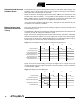
ATtiny28L/V Typical Characteristics The following charts show typical behavior. These figures are not tested during manufacturing. All current consumption measurements are performed with all I/O pins configured as inputs and with internal pull-ups enabled. A sine wave generator with railto-rail output is used as clock source. The power consumption in Power-down mode is independent of clock selection.
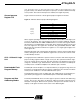
Figure 42. Active Supply Current vs. VCC ACTIVE SUPPLY CURRENT vs. VCC FREQUENCY = 4 MHz 8 7 TA = 25˚C 6 TA = 85˚C ICC (mA) 5 4 3 2 1 0 1.5 2 2.5 3 3.5 4 4.5 5 5.5 6 VCC (V) Figure 43. Active Supply Current vs. VCC, Device Clocked by Internal Oscillator ACTIVE SUPPLY CURRENT vs. Vcc DEVICE CLOCKED BY 1.2MHz INTERNAL RC OSCILLATOR 6 5 TA = 25˚C 4 I cc(mA) TA = 85˚C 3 2 1 0 1.5 2 2.5 3 3.5 4 4.5 5 5.
ATtiny28L/V Figure 44. Active Supply Current vs. VCC, Device Clocked by External 32 kHz Crystal ACTIVE SUPPLY CURRENT vs. VCC DEVICE CLOCKED BY 32 kHz CRYSTAL 4 3.5 TA = 25˚C 3 TA = 85˚C ICC (mA) 2.5 2 1.5 1 0.5 0 1.5 2 2.5 3 3.5 4 4.5 5 5.5 6 VCC (V) Figure 45. Idle Supply Current vs. Frequency IDLE SUPPLY CURRENT vs. FREQUENCY TA = 25˚C 4.5 VCC = 6.0V 4 VCC = 5.5V 3.5 VCC = 5.0V ICC (mA) 3 2.5 VCC = 4.5V VCC = 4.0V 2 VCC = 3.6V VCC = 3.3V VCC = 3.0V 1.5 1 VCC = 2.7V VCC = 2.4V 0.
Figure 46. Idle Supply Current vs. VCC IDLE SUPPLY CURRENT vs. VCC FREQUENCY = 4 MHz 1.4 1.2 TA = 85˚C TA = 25˚C ICC (mA) 1 0.8 0.6 0.4 0.2 0 1.5 2 2.5 3 3.5 4 4.5 5 5.5 6 VCC (V) Figure 47. Idle Supply Current vs. VCC, Device Clocked by Internal Oscillator IDLE SUPPLY CURRENT vs. Vcc DEVICE CLOCKED BY 1.2MHz INTERNAL RC OSCILLATOR 0.7 0.6 TA = 25˚C 0.5 TA = 85˚C I cc(mA) 0.4 0.3 0.2 0.1 0 1.5 2 2.5 3 3.5 4 4.5 5 5.
ATtiny28L/V Figure 48. Idle Supply Current vs. VCC, Device Clocked by External 32 kHz Crystal IDLE SUPPLY CURRENT vs. VCC DEVICE CLOCKED BY 32 kHz CRYSTAL 30 25 TA = 85˚C 20 ICC (µA) TA = 25˚C 15 10 5 0 1.5 2 2.5 3 3.5 4 4.5 5 5.5 6 VCC (V) Figure 49. Power-down Supply Current vs. VCC POWER-DOWN SUPPLY CURRENT vs. VCC WATCHDOG TIMER DISABLED 3 TA = 85˚C 2.5 ICC (µA) 2 TA = 70˚C 1.5 1 0.5 TA = 45˚C TA = 25˚C 0 1.5 2 2.5 3 3.5 4 4.5 5 5.
Figure 50. Power-down Supply Current vs. VCC POWER-DOWN SUPPLY CURRENT vs. VCC WATCHDOG TIMER ENABLED 70 60 50 TA = 25˚C ICC (µA) TA = 85˚C 40 30 20 10 0 1.5 2 2.5 3 3.5 4 4.5 5 5.5 6 VCC (V) Analog comparator offset voltage is measured as absolute offset. Figure 51. Analog Comparator Offset Voltage vs. Common Mode Voltage (VCC = 5V) 18 16 TA = 25˚C Offset Voltage (mV) 14 12 TA = 85˚C 10 8 6 4 2 0 0 0.5 1 1.5 2 2.5 3 3.5 4 4.
ATtiny28L/V Figure 52. Analog Comparator Offset Voltage vs. Common Mode Voltage (VCC = 2.7V) 10 TA = 25˚C Offset Voltage (mV) 8 6 TA = 85˚C 4 2 0 0 0.5 1 1.5 2 2.5 3 Common Mode Voltage (V) Figure 53. Analog Comparator Input Leakage Current (VCC = 6V; TA = 25°C) 60 50 IACLK (nA) 40 30 20 10 0 -10 0 0.5 1 1.5 2 2.5 3 3.5 4 4.5 5 5.5 6 6.
Figure 54. Calibrated Internal RC Oscillator Frequency vs. VCC CALIBRATED RC OSCILLATOR FREQUENCY vs. OPERATING VOLTAGE 1.28 TA = 25˚C 1.26 TA = 45˚C TA = 70˚C 1.24 TA = 85˚C 1.22 FRc (MHz) 1.2 1.18 1.16 1.14 1.12 1.1 2 2.5 3 3.5 4 4.5 5 5.5 6 Vcc(V) Figure 55. Watchdog Oscillator Frequency vs. VCC 1600 1400 TA = 25˚C 1200 TA = 85˚C FRC (kHz) 1000 800 600 400 200 0 1.5 2 2.5 3 3.5 4 4.5 5 5.
ATtiny28L/V Sink and source capabilities of I/O ports are measured on one pin at a time. Figure 56. Pull-up Resistor Current vs. Input Voltage (VCC = 5V) 120 TA = 25˚C 100 TA = 85˚C IOP (µA) 80 60 40 20 0 0 0.5 1 1.5 2 2.5 VOP (V) 3 3.5 4 4.5 5 Figure 57. Pull-up Resistor Current vs. Input Voltage (VCC = 2.7V) 30 TA = 25˚C 25 TA = 85˚C IOP (µA) 20 15 10 5 0 0 0.5 1 1.5 2 2.
Figure 58. I/O Pin Sink Current vs. Output Voltage. All pins except PA2 (VCC = 5V) 70 TA = 25˚C 60 TA = 85˚C IOL (mA) 50 40 30 20 10 0 0 0.5 1 1.5 2 2.5 3 VOL (V) Figure 59. I/O Pin Source Current vs. Output voltage (VCC = 5V) 20 TA = 25˚C 18 16 TA = 85˚C IOH (mA) 14 12 10 8 6 4 2 0 0 0.5 1 1.5 2 2.5 3 3.5 4 4.
ATtiny28L/V Figure 60. I/O Pin Sink Current vs. Output Voltage, All Pins Except PA2 (VCC = 2.7V) 25 TA = 25˚C 20 IOL (mA) TA = 85˚C 15 10 5 0 0 0.5 1 1.5 2 VOL (V) Figure 61. I/O Pin Source Current vs. Output Voltage (VCC = 2.7V) 6 TA = 25˚C 5 TA = 85˚C IOH (mA) 4 3 2 1 0 0 0.5 1 1.5 2 2.
Figure 62. PA2 I/O Pin Sink Current vs. Output Voltage (High Current Pin PA2; TA = 25°C) 90 VCC = 3.6V 80 70 VCC = 2.4V IOL (mA) 60 50 40 VCC = 1.8V 30 20 10 0 0 0.5 1 1.5 2 2.5 3 3.5 4 VOL (V) Figure 63. I/O Pin Input Threshold Voltage vs. VCC (TA = 25°C) 2.5 Threshold Voltage (V) 2 1.5 1 0.5 0 2.7 4.0 5.
ATtiny28L/V Figure 64. I/O Pin Input Hysteresis vs. VCC (TA = 25°C) 0.18 0.16 Input Hysteresis (V) 0.14 0.12 0.1 0.08 0.06 0.04 0.02 0 2.7 4.0 5.
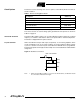
Register Summary Address Name Bit 7 Bit 6 Bit 5 Bit 4 Bit 3 Bit 2 Bit 1 Bit 0 Page $3F SREG I T H S V N Z C page 11 $3E Reserved Notes: 68 ...
ATtiny28L/V Instruction Set Summary Mnemonic Operands Description Operation Flags # Clocks ARITHMETIC AND LOGIC INSTRUCTIONS ADD Rd, Rr Add Two Registers Rd ← Rd + Rr Z,C,N,V,H ADC Rd, Rr Add with Carry Two Registers Rd ← Rd + Rr + C Z,C,N,V,H 1 SUB Rd, Rr Subtract Two Registers Rd ← Rd - Rr Z,C,N,V,H 1 SUBI Rd, K Subtract Constant from Register Rd ← Rd - K Z,C,N,V,H 1 SBC Rd, Rr Subtract with Carry Two Registers Rd ← Rd - Rr - C Z,C,N,V,H 1 SBCI Rd, K Subtract with Carr
Instruction Set Summary (Continued) Mnemonic Operands Description Operation Flags # Clocks DATA TRANSFER INSTRUCTIONS LD Rd, Z Load Register Indirect Rd ← (Z) None 2 ST Z, Rr Store Register Indirect (Z) ← Rr None 2 MOV Rd, Rr Move between Registers Rd ← Rr None 1 LDI Rd, K Load Immediate Rd =← K None 1 IN Rd, P In Port Rd ← P None 1 OUT P, Rr Out Port P ← Rr None 1 Load Program Memory R0 ←=(Z) None 3 LPM BIT AND BIT-TEST INSTRUCTIONS SBI P, b Set Bit in I/O Re
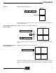
ATtiny28L/V Ordering Information Speed (MHz) Power Supply (Volts) Ordering Code Package Operation Range 4 2.7 - 5.5 ATtiny28L-4AC ATtiny28L-4PC ATtiny28L-4MC 32A 28P3 32M1-A Commercial (0°C to 70°C) ATtiny28L-4AI ATtiny28L-4PI ATtiny28L-4MI 32A 28P3 32M1-A Industrial (-40°C to 85°C) ATtiny28V-1AC ATtiny28V-1PC ATtiny28V-1MC 32A 28P3 32M1-A Commercial (0°C to 70°C) ATtiny28V-1AI ATtiny28V-1PI ATtiny28V-1MI 32A 28P3 32M1-A Industrial (-40°C to 85°C) 1.2 1.8 - 5.
Packaging Information 32A 32-lead, Thin (1.0mm) Plastic Quad Flatpack (TQFP), 7x7mm body, 2.0mm footprint, 0.8mm pitch. Dimensions in Millimeters and (Inches)* JEDEC STADARD MS-026 ABA 9.25 (0.364) 8.75 (0.344) PIN 1 ID 0.45 (0.018) 0.30 (0.012) PIN 1 9.25 (0.364) 8.75 (0.344) 0.80 (0.0315) BSC 7.10 (0.280) 6.90 (0.272) SQ 1.20 (0.047) MAX 0.20 (0.008) 0.09 (0.004) 0º~7º 0.75 (0.030) 0.45 (0.018) 0.15 (0.006) 0.05 (0.
ATtiny28L/V 28P3 28-lead, Plastic Dual Inline Package (PDIP), 0.300" Wide, (0.288" body width) Dimensions in Millimeters and (Inches)* 34.80(1.370) 34.54(1.360) 7.49(0.295) 7.11(0.280) 4.57(0.180)MAX 3.56(0.140) 3.05(0.120) 0.56(0.022) 2.54(0.100)BSC 1.65(0.065) 0.38(0.015) 1.27(0.050) 8.26(0.325) 7.62(0.300) 0º~ 15º REF 0.38(0.015) 10.20(0.400)MAX *Controlling dimension: Inches REV.
32M1-A D D1 PIN #1 ID 1 2 3 0 E1 E TOP VIEW A3 A2 P A1 D2 A 0.08 C PIN 1 ID SIDE VIEW 1 2 3 P COMMON DIMENSIONS (*Unit of Measure = mm) E2 SYMBOL MIN NOM MAX A 0.80 0.90 1.00 A1 0.00 0.02 0.05 A2 - 0.65 1.00 A3 e b b L BOTTOM VIEW NOTE 1. JEDEC STANDARD MO-220, Fig 2 (Anvil Singulation), VHHD-2 0.20 REF 0.18 D - E 5.00 BSC 4.75 BSC 1.25 e 74 0.30 4.75 BSC 1.25 E1 E2 R 0.23 5.00 BSC D1 D2 NOTE - 3.25 3.25 0.50 BSC L 0.30 0.40 0.50 P - - 0.
Atmel Headquarters Atmel Product Operations Corporate Headquarters Atmel Colorado Springs 2325 Orchard Parkway San Jose, CA 95131 TEL (408) 441-0311 FAX (408) 487-2600 Europe Atmel SarL Route des Arsenaux 41 Casa Postale 80 CH-1705 Fribourg Switzerland TEL (41) 26-426-5555 FAX (41) 26-426-5500 Asia Atmel Asia, Ltd. Room 1219 Chinachem Golden Plaza 77 Mody Road Tsimhatsui East Kowloon Hong Kong TEL (852) 2721-9778 FAX (852) 2722-1369 Japan Atmel Japan K.K. 9F, Tonetsu Shinkawa Bldg.