Features • Industry Standard Architecture – Low-cost Easy-to-use Software Tools • High-speed, Electrically-erasable Programmable Logic Devices – 7.
Description The ATF22V10B is a high-performance CMOS (electrically-erasable) programmable logic device (PLD) which utilizes Atmel’s proven electrically-erasable Flash memory technology. Speeds down to 7.5 ns and power dissipation as low as 10 mA are offered. All speed ranges are specified over the full 5V ± 10% range for military and industrial temperature ranges, and 5V ± 5% for commercial temperature ranges.
ATF22V10B(Q)(L) DC Characteristics Symbol Parameter Condition IIL Input or I/O Low Leakage Current 0 ≤ VIN ≤ VIL (Max) IIH Input or I/O High Leakage Current 3.5 ≤ VIN ≤ VCC ICC Power Supply Current, Standby VCC = Max, VIN = Max, Outputs Open Min Typ Max Units -35 -100 µA 10 µA Com. 85 120 mA Ind., Mil. 85 140 mA Com./Ind. 85/85 120/140 mA 85 140 mA 65/65 90/115 mA Mil. 65 115 mA Com. 65 90 mA Ind., Mil. 65 115 mA Com. 35 55 mA Com. 5 10 mA Ind.
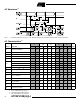
AC Waveforms(1) Note: 1. Timing measurement reference is 1.5V. Input AC driving levels are 0.0V and 3.0V, unless otherwise specified. AC Characteristics(1) -7 -10 -15 -20 -25 Min Max Min Max Min Max Min Max Min Max Units Input or Feedback to Combinatorial Output 3 7.5 3 10 3 15 3 20 3 25 ns tCO Clock to Output 2 4.5(2) 2 6.
ATF22V10B(Q)(L) Input Test Waveforms and Measurement Levels Output Test Loads Commercial Military tR, tF < 3 ns * All except -7 which is R2 = 300Ω Pin Capacitance f = 1 MHz, T = 25°C(1) Typ Max Units CIN 5 8 pF VIN = 0V COUT 6 8 pF VOUT = 0V Note: Conditions 1. Typical values for nominal supply voltage. This parameter is only sampled and is not 100% tested. Power-up Reset The registers in the ATF22V10Bs are designed to reset during power-up.
Electronic Signature Word Input and I/O Pull-ups There are 64 bits of programmable memory that are always available to the user, even if the device is secured. These bits can be used for user-specific data. All ATF22V10B family members have internal input and I/O pull-up resistors. Therefore, whenever inputs or I/Os are not being driven externally, they will float to V CC . This ensures that all logic array inputs are at known states.
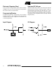
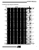
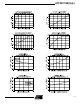
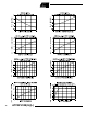
ATF22V10B(Q)(L) Functional Logic Diagram ATF22V10B 7
ATF22V10B(Q)(L)
ATF22V10B(Q)(L) 9
ATF22V10B(Q)(L)
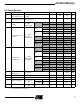
ATF22V10B(Q)(L) ATF22V10B Ordering Information tPD (ns) tS (ns) tCO (ns) Ordering Code Package (1) Operation Range 7.5 3.5 4.5 ATF22V10B-7JC ATF22V10B-7PC(1) ATF22V10B-7SC(1) ATF22V10B-7XC(1) 28J 24P3 24S 24X Commercial (0°C to 70°C) 10 4.5 6.
ATF22V10BQ(L) Ordering Information tPD (ns) tCO (ns) Ordering Code Package (1) Operation Range 15 10 8 ATF22V10BQ-15JC ATF22V10BQ-15PC(1) ATF22V10BQ-15SC(1) ATF22V10BQ-15XC(1) 28J 24P3 24S 24X Commercial (0°C to 70°C) 20 14 12 ATF22V10BQL-20JC(1) ATF22V10BQL-20PC(1) ATF22V10BQL-20SC(1) ATF22V10BQL-20XC(1) 28J 24P3 24S 24X Commercial (0°C to 70°C) ATF22V10BQL-20JI(1) ATF22V10BQL-20PI(1) ATF22V10BQL-20SI(1) ATF22V10BQL-20XI(1) 28J 24P3 24S 24X Industrial (-40°C to 85°C) ATF22V10BQL-20GM/88
ATF22V10B(Q)(L) Using “C” Product for Industrial To use commercial product for Industrial temperature ranges, down-grade one speed grade from the “I” to the “C” device (7 ns “C” = 10 ns “I”) and de-rate power by 30%. Package Type 24D3 24-pin, 0.300" Wide, Ceramic Dual Inline Package (Cerdip) 28J 28-lead, Plastic J-leaded Chip Carrier (PLCC) 28L 28-pad, Ceramic Leadless Chip Carrier (LCC) 24P3 24-pin, 0.300" Wide, Plastic Dual Inline Package (PDIP) 24S 24-lead, 0.
Packaging Information 24D3, 24-pin, 0.300" Wide, Non-windowed, Ceramic Dual Inline Package (Cerdip) Dimensions in Inches and (Millimeters) 28J, 28-lead, Plastic J-leaded Chip Carrier (PLCC) Dimensions in Inches and (Millimeters) JEDEC STANDARD MS-018 AB MIL-STD-1835 D-9 CONFIG A 1.28(32.5) 1.24(31.5) .045(1.14) X 45° PIN NO. 1 IDENTIFY PIN 1 .310(7.87) .285(7.24) .098(2.49) MAX .005(.127) MIN 1.100(27.94) REF .200(5.08) MAX SEATING PLANE .015(.381) .008(.203) .032(.813) .026(.660) .065(1.65) .
ATF22V10B(Q)(L) Packaging Information 24S, 24-lead, 0.300" Wide, Plastic Gull Wing Small Outline (SOIC) Dimensions in Inches and (Millimeters) 24X, 24-lead, 4.4 mm Wide, Plastic Thin Shrink Small Outline (TSSOP) Dimensions in Millimeters and (Inches) .020(.508) .013(.330) .299(7.60) .420(10.7) .291(7.39) .393(9.98) PIN 1 ID .050(1.27) BSC .616(15.6) .598(15.2) .105(2.67) .092(2.34) .012(.305) .003(.076) .013(.330) .009(.229) 0 REF 8 .050(1.27) .015(.
Atmel Headquarters Atmel Operations Corporate Headquarters Atmel Colorado Springs 2325 Orchard Parkway San Jose, CA 95131 TEL (408) 441-0311 FAX (408) 487-2600 Europe 1150 E. Cheyenne Mtn. Blvd. Colorado Springs, CO 80906 TEL (719) 576-3300 FAX (719) 540-1759 Atmel Rousset Atmel SarL Route des Arsenaux 41 Casa Postale 80 CH-1705 Fribourg Switzerland TEL (41) 26-426-5555 FAX (41) 26-426-5500 Asia Atmel Asia, Ltd.