
User guide

1
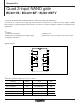
Standard ICs
Quad 2-input NAND gate
BU4011B / BU4011BF / BU4011BFV
The BU4011B, BU4011BF, and BU4011BFV are dual-input positive logic NAND gates.
Four circuits are contained on a single chip. An inverter-based buffer has been added to the gate output, enabling
improved input / output propagation characteristics, and an increased load capacitance minimizes fluctuation in prop-
agation time.
•
Features
1) Low power dissipation.
2) Wide range of operating power supply voltage.
3) High input impedance.
4) High fan-out.
5) Direct drive of 2 L-TTL inputs and 1 LS-TTL input.
•
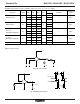
Block diagram
A1
B1
O1
O2
B2
A2
1
2
3
4
5
6
7V
SS
14
13
12
11
10
9
8
VDD
A4
B4
O4
O3
B3
A3
•
Absolute maximum ratings (VSS = 0V, Ta = 25°C)
Parameter Limits
Power supply voltage
Power dissipation
Operating temperature
Storage temperature
Input voltage
Symbol
V
DD
Pd
Topr
Tstg
V
IN
Unit
V
mW
°C
°C
V
– 0.3 ~ + 18
– 40 ~ + 85
– 55 ~ + 150
– 0.3 ~ V
DD + 0.3
1000 (DIP), 450 (SOP)
350 (SSOP-B14)