
User Manual

1
Standard ICs
Hex inverter
BU4069UB / BU4069UBF / BU4069UBFV
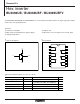
The BU4069UB, BU4069UBF and BU4069UBFV are six-circuit inverters with no buffers. A single-stage gate configu-
ration reduces the propagation time.
•
Logic circuit diagram
•
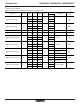
Absolute maximum ratings (VSS = 0V, Ta = 25°C)
VDD
OUT
VSS
IN
Parameter
Limits
Power supply voltage
Power dissipation
Operating temperature
Storage temperature
Input voltage
Symbol
V
DD
Pd
Topr
Tstg
V
IN
Unit
V
mW
°C
°C
V
– 0.3 ~ + 18
– 40 ~ + 85
– 55 ~ + 150
– 0.3 ~ V
DD + 0.3
1000 (DIP), 450 (SOP), 350 (SSOP-B14)
•
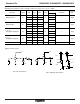
Block diagram
1
I
1
2
O
1
3
I
2
4
O
2
5
I
3
6
O
3
7
14
13
12
11
10
9
8
V
SS
VDD
I6
O6
I5
O5
I4
O4
•
Features
1) Low power dissipation.
2) Wide range of operating power supply voltages.
3) High input impedance.
4) High fan-out.
5) Direct drive of 2 L-TTL inputs and 1 LS-TTL input.