
Manual


1
Standard ICs
Single OR gate
BU4S71
The BU4S71 is an ultra-compact IC with one circuit of the dual-input positive logic OR gate built into an SMP pack-
age.
•
Features
1) Low current dissipation.
2) Super-mini mold package designed for surface
mounting.
3) Wide range of operating power supply voltage.
4) Direct drive of 2 L-TTL inputs and 1 LS-TTL input.
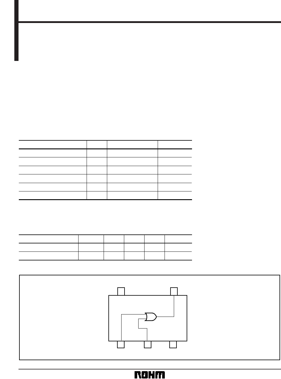
•
Block diagram
•
Recommended operating conditions (Ta = 25°C, VSS = 0V)
54
123
V
DD Y
ABV
SS
Parameter Symbol Min. Typ. Max. Unit
V
DD 3
—
16 V
V
IN 0
—
VDD V
Power supply voltage
Input voltage
•
Absolute maximum ratings (Ta = 25°C)
Parameter Symbol Limits Unit
V
DD VSS – 0.3 ~ VSS + 18 V
170 mW
I
IN mA
Topr
V
IN V
Tstg
Pd
Power supply voltage
Power dissipation
Input current
Operating temperature
Storage temperature
Input voltage
Note 1: These values indicate the range limits of the voltage that can be applied to each pin without
destroying it. Operation is not guaranteed at these values.
Note 2: Reduced by 1.7mW for each increase in Ta of 1°C over 25°C.
± 10
V
SS – 0.3 ~ VDD + 0.3
°C
°C
– 40 ~ + 85
– 55 ~ + 150