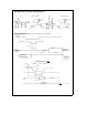
ADC0801/ADC0802/ADC0803/ADC0804/ADC0805 8-Bit mP Compatible A/D Converters General Description The ADC0801, ADC0802, ADC0803, ADC0804 and ADC0805 are CMOS 8-bit successive approximation A/D converters that use a differential potentiometric ladderÐ similar to the 256R products. These converters are designed to allow operation with the NSC800 and INS8080A derivative control bus with TRI-STATEÉ output latches directly driving the data bus.
Absolute Maximum Ratings (Notes 1 & 2) Storage Temperature Range If Military/Aerospace specified devices are required, please contact the National Semiconductor Sales Office/Distributors for availability and specifications. 875 mW ESD Susceptibility (Note 10) Supply Voltage (VCC) (Note 3) 6.5V Voltage b 0.3V to a 18V Logic Control Inputs b 0.3V to (VCC a 0.3V) At Other Input and Outputs Lead Temp.
AC Electrical Characteristics (Continued) The following specifications apply for VCC e 5VDC and TMIN s TA s TMAX, unless otherwise specified. Symbol Parameter Conditions Min Typ Max Units CONTROL INPUTS [Note: CLK IN (Pin 4) is the input of a Schmitt trigger circuit and is therefore specified separately] VIN (0) Logical ‘‘0’’ Input Voltage (Except Pin 4 CLK IN) VCC e 4.
Typical Performance Characteristics Logic Input Threshold Voltage vs. Supply Voltage Delay From Falling Edge of RD to Output Data Valid vs. Load Capacitance CLK IN Schmitt Trip Levels vs. Supply Voltage fCLK vs. Clock Capacitor Full-Scale Error vs Conversion Time Effect of Unadjusted Offset Error vs.
TRI-STATE Test Circuits and Waveforms t1H t1H, CL e 10 pF t0H tr e 20 ns t0H, CL e 10 pF tr e 20 ns TL/H/5671 – 3 Timing Diagrams (All timing is measured from the 50% voltage points) Output Enable and Reset INTR Note: Read strobe must occur 8 clock periods (8/fCLK) after assertion of interrupt to guarantee reset of INTR.
Typical Applications (Continued) 6800 Interface Ratiometric with Full-Scale Adjust Note: before using caps at VIN or VREF/2, see section 2.3.2 Input Bypass Capacitors. Absolute with a 2.500V Reference Absolute with a 5V Reference *For low power, see also LM385-2.
Typical Applications (Continued) A mP Interfaced Comparator Directly Converting a Low-Level Signal For: VIN( a ) l VIN( b ) Output e FFHEX VREF/2 e 256 mV For: VIN( a ) k VIN( b ) Output e 00HEX 1 mV Resolution with mP Controlled Range VREF/2 e 128 mV 1 LSB e 1 mV VDAC s VIN s (VDAC a 256 mV) Digitizing a Current Flow TL/H/5671 – 6 7
Typical Applications (Continued) External Clocking Self-Clocking Multiple A/Ds 100 kHz s fCLK s 1460 kHz *Use a large R value to reduce loading at CLK R output. mP Interface for Free-Running A/D Self-Clocking in Free-Running Mode *After power-up, a momentary grounding of the WR input is needed to guarantee operation. Operating with ‘‘Automotive’’ Ratiometric Transducers Ratiometric with VREF/2 Forced *VIN( b ) e 0.
Typical Applications (Continued) mP Compatible Differential-Input Comparator with Pre-Set VOS (with or without Hysteresis) *See Figure 5 to select R value DB7 e ‘‘1’’ for VIN( a ) l VIN( b ) a (VREF/2) Omit circuitry within the dotted area if hysteresis is not needed Handling g 10V Analog Inputs Low-Cost, mP Interfaced, Temperature-to-Digital Converter *Beckman Instruments Ý694-3-R10K resistor array mP Interfaced Temperature-to-Digital Converter *Circuit values shown are for 0§ C s TA s a 128§ C **Can
Typical Applications (Continued) Handling g 5V Analog Inputs Read-Only Interface TL/H/5671 – 34 TL/H/5671–33 *Beckman Instruments Ý694-3-R10K resistor array mP Interfaced Comparator with Hysteresis Protecting the Input Diodes are 1N914 TL/H/5671 – 9 A Low-Cost, 3-Decade Logarithmic Converter TL/H/5671–35 Analog Self-Test for a System TL/H/5671–36 *LM389 transistors A, B, C, D e LM324A quad op amp 10 TL/H/5671 – 37
Typical Applications (Continued) 3-Decade Logarithmic A/D Converter Multiplexing Differential Inputs Noise Filtering the Analog Input fC e 20 Hz Uses Chebyshev implementation for steeper roll-off unity-gain, 2nd order, low-pass filter Adding a separate filter for each channel increases system response time if an analog multiplexer is used Increasing Bus Drive and/or Reducing Time on Bus Output Buffers with A/D Data Enabled TL/H/5671 – 10 *A/D output data is updated 1 CLK period prior to assertion of
Typical Applications (Continued) Sampling an AC Input Signal Note 1: Oversample whenever possible [keep fs l 2f( b 60)] to eliminate input frequency folding (aliasing) and to allow for the skirt response of the filter. Note 2: Consider the amplitude errors which are introduced within the passband of the filter. 70% Power Savings by Clock Gating (Complete shutdown takes & 30 seconds.) Power Savings by A/D and VREF Shutdown TL/H/5671 – 11 *Use ADC0801, 02, 03 or 05 for lowest power consumption.
Functional Description other words, if we apply an analog input equal to the centervalue g (/4 LSB, we guarantee that the A/D will produce the correct digital code. The maximum range of the position of the code transition is indicated by the horizontal arrow and it is guaranteed to be no more than (/2 LSB. The error curve of Figure 1c shows a worst case error plot for the ADC0802.
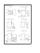
Functional Description (Continued) A functional diagram of the A/D converter is shown in Figure 2 . All of the package pinouts are shown and the major logic control paths are drawn in heavier weight lines. The converter is started by having CS and WR simultaneously low. This sets the start flip-flop (F/F) and the resulting ‘‘1’’ level resets the 8-bit shift register, resets the Interrupt (INTR) F/F and inputs a ‘‘1’’ to the D flop, F/F1, which is at the input end of the 8-bit shift register.
Functional Description (Continued) slight time difference between the input voltage samples is given by: After the ‘‘1’’ is clocked through the 8-bit shift register (which completes the SAR search) it appears as the input to the D-type latch, LATCH 1. As soon as this ‘‘1’’ is output from the shift register, the AND gate, G2, causes the new digital word to transfer to the TRI-STATE output latches.
Functional Description (Continued) resistance and the use of an input bypass capacitor. This error can be eliminated by doing a full-scale adjustment of the A/D (adjust VREF/2 for a proper full-scale readingÐsee section 2.5.2 on Full-Scale Adjustment) with the source resistance and input bypass capacitor in place.
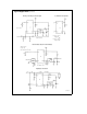
Functional Description (Continued) *Add if VREF/2 s 1 VDC with LM358 to draw 3 mA to ground. TL/H/5671 – 16 a) Analog Input Signal Example b) Accommodating an Analog Input from 0.5V (Digital Out e e 00HEX) to 3.5V (Digital Out e FFHEX) FIGURE 5. Adapting the A/D Analog Input Voltages to Match an Arbitrary Input Signal Range 2.5 Errors and Reference Voltage Adjustments 2.4.2 Reference Accuracy Requirements The converter can be operated in a ratiometric mode or an absolute mode.
Functional Description (Continued) conversion in process is not allowed to be completed, therefore the data of the previous conversion remains in this latch. The INTR output simply remains at the ‘‘1’’ level. 2.5.3 Adjusting for an Arbitrary Analog Input Voltage Range If the analog zero voltage of the A/D is shifted away from ground (for example, to accommodate an analog input signal that does not go to ground) this new zero reference should be properly adjusted first.
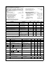
Functional Description (Continued) VREF/2 e 2.560V) can be determined. For example, for an output LED display of 1011 0110 or B6 (in hex), the voltage values from the table are 3.520 a 0.120 or 3.640 VDC. These voltage values represent the center-values of a perfect A/D converter. The effects of quantization error have to be accounted for in the interpretation of the test results. For a higher speed test system, or to obtain plotted data, a digital-to-analog converter is needed for the test set-up.
Functional Description (Continued) FIGURE 8. A/D Tester with Analog Error Output TL/H/5671 – 19 FIGURE 9. Basic ‘‘Digital’’ A/D Tester TABLE I. DECODING THE DIGITAL OUTPUT LEDs HEX OUTPUT VOLTAGE CENTER VALUES WITH VREF/2 e 2.
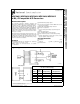
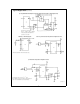
Functional Description (Continued) TL/H/5671 – 20 Note 1: *Pin numbers for the DP8228 system controller, others are INS8080A. Note 2: Pin 23 of the INS8228 must be tied to a 12V through a 1 kX resistor to generate the RST 7 instruction when an interrupt is acknowledged as required by the accompanying sample program. FIGURE 10.
Functional Description (Continued) It is important to note that in systems where the A/D converter is 1-of-8 or less I/O mapped devices, no address decoding circuitry is necessary. Each of the 8 address bits (A0 to A7) can be directly used as CS inputsÐone for each I/O device.
ready decoded 4/5 line is brought out to the common bus at pin 21. This can be tied directly to the CS pin of the A/D, provided that no other devices are addressed at HX ADDR: 4XXX or 5XXX. Functional Description (Continued) 4.2 Interfacing the Z-80 The Z-80 control bus is slightly different from that of the 8080.
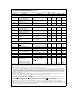
Functional Description (Continued) 0010 0012 0015 0018 001B 001C 001D 001F 0022 0024 0027 0028 002A 002C 002E 0031 0033 0034 0036 0038 003B 003D 003F SAMPLE PROGRAM FOR FIGURE 14 ADC0801-MC6800 CPU INTERFACE DF 36 DATAIN STX TEMP2 ; Save contents of X CE 00 2C LDX #$002C ; Upon IRQ low CPU FF FF F8 STX $FFF8 ; jumps to 002C B7 50 00 STAA $5000 ; Start ADC0801 0E CLI 3E CONVRT WAI ; Wait for interrupt DE 34 LDX TEMP1 8C 02 0F CPX #$020F ; Is final data stored? 27 14 BEQ ENDP B7 50 00 STAA $5000 ; Restarts A
Functional Description (Continued) SAMPLE PROGRAM FOR FIGURE 15 ADC0801 – MC6820 PIA INTERFACE 0010 0013 0016 0019 001A 001D 0020 0021 0023 0025 0028 002B 002C 002E 0031 0033 0034 0036 0038 003A 003D 003F 0040 CE 00 38 FF FF F8 B6 80 06 4F B7 80 07 B7 80 06 0E C6 34 86 3D F7 80 07 B7 80 07 3E DE 40 8C 02 0F 27 0F 08 DF 40 20 ED DE 40 B6 80 06 A7 00 3B 02 00 0042 0045 0047 CE 02 00 DF 40 39 DATAIN CONVRT INTRPT TEMP1 ENDP PIAORB PIACRB LDX STX LDAA CLRA STAA STAA CLI LDAB LDAA STAB STAA WAI LDX CPX
Functional Description (Continued) Note 1: Numbers in parentheses refer to MC6800 CPU pin out. Note 2: Numbers of letters in brackets refer to standard M6800 system common bus code. TL/H/5671 – 26 FIGURE 16.
Functional Description (Continued) SAMPLE PROGRAM FOR FIGURE 16 INTERFACING MULTIPLE A/Ds IN AN MC6800 SYSTEM ADDRESS HEX CODE MNEMONICS COMMENTS 0033 A7 00 STAA X ; Store data at X 0035 8C 02 07 CPX #$0207 ; Have all A/D’s been read? 0038 27 05 BEQ RETURN ; Yes: branch to RETURN 003A 08 INX ; No: increment X by one 003B DF 42 STX INDEX2 ; X x INDEX2 003D 20 EB BRA INTRPT ; Branch to 002A 003F 3B RETURN RTI 0040 50 00 INDEX1 FDB $5000 ; Starting address for A/D 0042 02 00 INDEX2 FDB $0200 ; Starting address
Functional Description (Continued) Note 1: R2 e 49.5 R1 Note 2: Switches are LMC13334 CMOS analog switches. Note 3: The 9 resistors used in the auto-zero section can be g 5% tolerance. FIGURE 17. Gain of 100 Differential Transducer Preamp TL/H/5671 – 27 FIGURE 18.
A flow chart for the zeroing subroutine is shown in Figure 19 . It must be noted that the ADC0801 series will output an all zero code when it converts a negative input [VIN(b) t VIN( a )]. Also, a logic inversion exists as all of the I/O ports are buffered with inverting gates. Basically, if the data read is zero, the differential output voltage is negative, so a bit in Port B is cleared to pull VX more negative which will make the output more positive for the next conversion.
3D00 3D02 3D04 3D06 3D07 3D09 3D0B 3D0D 3D0E 3D10 3D13 3D15 3D16 3D17 3D1A 3D1B 3D1D 3D20 3D21 3D23 3D24 3D26 3D29 3D2A 3D2D 3D2E 3D2F 3D30 3D33 3D34 3D37 3D38 3D39 3D3B 3D3D 3C3D 3C3F 3C41 3C42 3C43 3C45 3C48 3E90 D3E7 2601 7C D3E6 0680 3E7F 4F D3E5 31AA3D D3E4 FB 00 C3163D 7A C600 CA2D3D 78 F600 1F FE00 CA373D 47 C3333D 79 B0 4F C3203D A9 C30D3D 47 7C EE03 D3E6 MVI 90 Out Control Port MVI H 01 MOV A,H OUT C MVI B 80 MVI A 7F MOV C,A OUT B LXI SP 3DAA OUT A IE NOP JMP Loop MOV A,D ADI 00 JZ Set C MOV A,
TL/H/5671 – 29 FIGURE 21. Multiple A/Ds with Z-80 Type Microprocessor INTERRUPT SERVICING SUBROUTINE SOURCE LOC OBJ CODE STATEMENT COMMENT 0038 E5 PUSH HL ; Save contents of all registers affected by 0039 C5 PUSH BC ; this subroutine. 003A F5 PUSH AF ; Assumed INT mode 1 earlier set. 003B 21 00 3E LD (HL),X3E00 ; Initialize memory pointer where data will be stored. 003E 0E 01 LD C, X01 ; C register will be port ADDR of A/D converters. 0040 D300 OUT X00, A ; Load peripheral status word into 8-bit latch.
Ordering Information 0§ C TO 70§ C TEMP RANGE ERROR g (/4 Bit Adjusted g (/2 Bit Unadjusted g (/2 Bit Adjusted g 1Bit Unadjusted 0§ C TO 70§ C 0§ C TO 70§ C b 40§ C TO a 85§ C ADC0801LCN PACKAGE OUTLINE ADC0802LCWM ADC0802LCV ADC0802LCN ADC0803LCWM ADC0803LCV ADC0803LCN ADC0804LCWM ADC0804LCV M20BÐSmall Outline V20AÐChip Carrier TEMP RANGE g (/4 Bit Adjusted ERROR g (/2 Bit Unadjusted g (/2 Bit Adjusted g 1Bit Unadjusted PACKAGE OUTLINE ADC0804LCN ADC0805LCN N20AÐMolded DIP b 40§ C
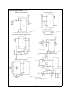
Physical Dimensions inches (millimeters) Dual-In-Line Package (J) Order Number ADC0801LJ, ADC0802LJ, ADC0801LCJ, ADC0802LCJ, ADC0803LCJ or ADC0804LCJ ADC0802LJ/883 or 5962-9096601MRA NS Package Number J20A SO Package (M) Order Number ADC0802LCWM, ADC0803LCWM or ADC0804LCWM NS Package Number M20B 34
Physical Dimensions inches (millimeters) (Continued) Molded Dual-In-Line Package (N) Order Number ADC0801LCN, ADC0802LCN, ADC0803LCN, ADC0804LCN or ADC0805LCN NS Package Number N20A 35
ADC0801/ADC0802/ADC0803/ADC0804/ADC0805 8-Bit mP Compatible A/D Converters Physical Dimensions inches (millimeters) (Continued) Molded Chip Carrier Package (V) Order Number ADC0802LCV, ADC0803LCV or ADC0804LCV NS Package Number V20A LIFE SUPPORT POLICY NATIONAL’S PRODUCTS ARE NOT AUTHORIZED FOR USE AS CRITICAL COMPONENTS IN LIFE SUPPORT DEVICES OR SYSTEMS WITHOUT THE EXPRESS WRITTEN APPROVAL OF THE PRESIDENT OF NATIONAL SEMICONDUCTOR CORPORATION. As used herein: 1.